
CONTENTS
36.2.2 Basic CNT Film Fabrication
36.2.3 Basic CNT Film Characterization
36.3.1 Basic Film Characteristics
36.3.2 Effect of Process Parameter
36.3.2.1 Sonication Time and CNT Distribution
36.3.2.2 Chemical Treatment with Concentrated HNO3
36.3.2.3 Optical Characteristics
36.3.3 CNT Networks for Gas Sensing
Random carbon nanotube (CNT) networks have raised a continuously increasing interest among a broad and multidisciplinary community of researchers over the last decade. The remarkable and concurrently diverse properties of such networks have rendered them suitable for a wide range of applications in science and engineering. Among the most promising applications are transparent conductive electrodes [1, 2 and 3], thin-film transistors and circuits [4,5], and mechanical and chemical sensors [6, 7 and 8]. The desired functionality of the CNT films produced for different applications depends primarily on the choice of the appropriate raw material. Nevertheless, it is strongly influenced by major process-specific aspects. A random CNT network can either be directly grown by chemical vapor deposition (CVD) or processed from a solution of well-dispersed nanotubes. The CVD process involves catalyst nanoparticles acting as seeds for the growth of the CNTs. Although this method leads to films with individually separated tubes and better inter-tube junctions, it is a high vacuum/temperature process that is not suitable for the emerging field of low-cost flexible electronics. Solution-based methods, on the other hand, have several advantages. In general, relying on this kind of low-temperature processes overrides most constraints on the choice of the substrate material, enabling fabrication even on plastic substrates. The omission of a high-vacuum process further reduces costs significantly.
A significant step toward the commercialization of novel CNT electronics involves the development of large-area and high-throughput processes for the fabrication of high-quality CNT films. Among all the different fabrication techniques available, spray deposition is considered to be one of the most competitive in terms of the cost–performance ratio. It offers the means for depositing CNT films with high uniformity and low roughness over large areas in a high-throughput (inline) process. The successful adoption of this technique to CNT film fabrication for various applications has been previously reported in the literature [3,9].
In this chapter, we demonstrate a reliable and reproducible spray deposition process for the fabrication of CNT films exhibiting state-of-the-art performance. The convenient control of major process parameters enables a fine and accurate tuning of film characteristics, hence rendering this process suitable for a wide range of device applications with different requirements. Films that are fabricated using this process are further applied as resistive networks in gas-sensing devices. We demonstrate that such devices, incorporating highly uniform pristine CNT films, exhibit a high sensitivity toward ammonia (NH3) without the need for any further functionalization of the CNT film, thereby maintaining a simple fabrication process.
Spray technology is used in a wide variety of applications such as surface coating, humidification, combustion, and others. Each application area requires different spray nozzles to fulfill the specified criteria and achieve the desired results. The layers deposited here were sprayed by an air atomizing nozzle. This type of nozzles provides, along with ultrasonic spray nozzles, the finest degree of atomization. It is worth mentioning that ultrasonic spray nozzles have also been successfully applied to the deposition of high-uniformity CNT films [3]. For our static test system, a commercially available automatic air atomizing spray gun (Krautzberger GmbH, Germany) was used. The spray gun contains an internal pneumatic control system that is activated by an electromechanical 3/2-way valve connected to a timer for precise spray time adjustment. Other major spray parameters to be adjusted for obtaining the desired spray characteristics are the material flow rate, atomizing gas (N2) pressure, nozzle-to-sample distance, and substrate temperature. For air-assisted nozzles, the diameter of the orifice is one of the most significant dimensions for atomization. Here, a nozzle with a 0.5 mm orifice diameter was chosen. The atomizing gas (N2) pressure was kept below 1 bar throughout all experiments in order to obtain the desired spray characteristics and a uniform spray pattern across the area of interest. We use an approach introduced previously for the spray deposition of active polymers in organic photodiodes [10,11], in which we operate within the wet spraying regime while heating up the substrate in order to speed up the drying of wet droplets arriving at the substrate. This approach allows the formation of dry layers with good thickness control over time, enhancing at the same time reproducibility. Figure 36.1a shows a schematic drawing of the test setup, indicating the vertical arrangement of a nozzle and a substrate.
To disperse CNTs in an aqueous solution, a high molecular weight cellulose derivative, sodium carboxymethyl cellulose (CMC), is used. This kind of dispersant has been reported previously as an excellent agent for dispersing single-walled nanotubes (SWNTs) in water [12]. As a first step, an adequate quantity of CMC is added to Millipore DI water so as to obtain a 0.5 wt% aqueous solution of CMC. This solution is then stirred for ≥12 h at room temperature to uniformly dissolve the surfactant in water. The desired amount of SWNTs can then be added to the previously prepared CMC stock solution. Typically, a concentration between 0.03 and 0.05 wt% of SWNTs is used. Actual dispersion of the CNTs is achieved by sonication of the complete solution for 90 min in a bath sonicator. For dispersions prepared by probe sonication, the duration is reduced to 15 min. The solution is then centrifuged at 15,000 rpm for 2 h and the final solution is obtained by decanting the top 80% of the supernatant.
36.2.2 BASIC CNT FILM FABRICATION
For the fabrication of highly uniform and smooth CNT films, the final CNT solution is spray deposited onto plain glass substrates. Prior to film deposition, the substrates are thoroughly cleaned by sonication in acetone and isopropanol. The substrates are then exposed to oxygen plasma for further cleaning and surface treatment. An increased wettability of the glass surface after plasma treatment is beneficial for achieving uniform surface coating during spray deposition of the water-based CNT solution. Chemical post-deposition treatment is necessary to remove the CMC-matrix embedding the CNTs, thus changing the film behavior from insulating to conductive. For this purpose, samples are immersed in dilute HNO3 (13–23%) for ≥24 h at room temperature. Some samples are additionally immersed in concentrated HNO3 (65%) for 1 h to further increase conductivity via stronger doping of CNTs [3,9]. Samples are finally rinsed in DI water and subsequently dried. Note that all steps involved in CNT film fabrication are performed entirely in ambient conditions.
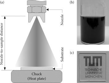
FIGURE 36.1 (a) Schematic drawing of the test setup, indicating the vertical arrangement of a nozzle and a substrate. (b) Vial containing a CNT/surfactant aqueous dispersion after sonication and centrifugation, ready for deposition. (c) An image of a CNT film on glass, uniformly deposited over an area of 1 cm2. (A. Abdellah et al., IEEE-NANO 2011, 11th IEEE Conference on Nanotechnology 2011, Portland, OR, pp.1118–1123. © (2011) IEEE. With permission.)
36.2.3 BASIC CNT FILM CHARACTERIZATION
The surface characterization and thickness measurements of fabricated CNT films were performed with an atomic force microscope (AFM) operated in a tapping mode. Information on CNT length distribution was extracted from AFM images of low-density films using image processing software (ImageJ). Sheet resistances were measured using a four-point collinear probe method on a Keithley 4200 semiconductor parameter analyzer. Optical transmission was measured using a chopped 300 W xenon arc research source passing through an Oriel Cornerstone 260 1/4 m monochromator and a calibrated silicon photodiode with a preamplifier connected to an Oriel Merlin digital lock-in radiometry system.
36.3.1 BASIC FILM CHARACTERISTICS
Prior to the adoption of CNT films in any specific application, it is necessary to optimize and evaluate the elementary film performance on the basis of some primary figures of merit and their dependence on different process parameters. Among the most important figures are sheet resistance or conductivity, optical transmittance or absorption spectra, mechanical stability, CNT distribution, and surface characteristics. For this reason, we first present an overview of basic film performance and the means for controlling the same before discussing the device-specific aspects of gas sensors as one possible application of such CNT films.
As already mentioned in the previous section, we use CMC as a surfactant to aid dispersion of the nanotubes in water. This implies that the surfactant will still be present in all deposited films before performing further post-deposition treatments. As-prepared films are therefore composed of a CNT network embedded into a CMC-matrix. Single CNTs and CNT-bundles are suspended within the insulating matrix, and hence the film does not exhibit any conductive behavior. Figure 36.2a shows an optical microscopy image of an as-prepared film. Note the clearly distinguishable disk-like structures typical for spray-deposited layers. Droplets are deformed upon impact onto the substrate and dry rapidly creating the features observed. After removal of the CMC-matrix, the suspended CNT network embedded in the matrix collapses, thereby forming the final film of directly interconnected CNTs and exhibiting conductive behavior. This is achieved by chemical post-deposition treatment as described in the experimental section. An optical microscopy image of such a pristine CNT film is shown in Figure 36.2b. It is clear from the image that the features previously observed in as-prepared films completely vanish after CMC removal. Moreover, the film seems highly uniform with no agglomerates or other clear particles visible at an optical scale.
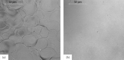
FIGURE 36.2 (a) Optical microscopy image of an as-prepared film, showing disk-like features originating from spray deposition. (b) The same film after removal of the surfactant matrix. The final film of directly interconnected CNTs is formed and exhibits a conductive behavior. (A. Abdellah et al., IEEE-NANO 2011, 11th IEEE Conference on Nanotechnology 2011, Portland, OR, pp.1118–1123. © (2011) IEEE. With permission.)
An accurate examination of the surface characteristics at the nano-scale is required for a detailed evaluation of the pristine CNT film quality. This involves the characterization of uniformity, surface roughness, and CNT length distribution. Surface roughness is of especially great significance as it can become a crucial factor in certain applications, for example, when considering these films as transparent electrodes for optoelectronic devices. The CNT length distribution, on the other hand, is of relevance for the evaluation of the dispersion quality and an understanding of the contribution of different process steps in altering the physical properties of the raw CNT material. Sonication during the solution preparation was shown to shorten the CNTs and has therefore to be carefully optimized in terms of power and duration [13]. Figure 36.3 shows two AFM images of the film introduced in Figure 36.1c, scanned over a large area of 10 × 10 μm2 (left image) as well as a zoom-in of a smaller area of 2 × 2 μm2 (right image). For the 10 × 10 μm2 scan, the values measured for the average and RMS surface roughness are 5.79 and 7.41 nm, respectively. Very similar values (5.64 and 7.13 nm) are obtained from the 2 × 2 μm2 scan, which demonstrates a high uniformity of the films independent of the total area under investigation.
Another major figure of merit necessary toward a full characterization of CNT films is the sheet resistance (Rsh) or DC conductivity (σdc) and its dependence on the film thickness (d) or density. Owing to the percolating nature of the CNT films, Rsh is expected to vary inversely with film density. Since CNT density is correlated to film thickness, Rsh is also expected to scale inversely with film thickness. Figure 36.4a plots the relation between Rsh, as determined by four-point probe measurements, and d. One can clearly observe the reduction in sheet resistance with increasing film thickness or density, reaching as low as 60 Ω/sq at approx. 42 nm. DC conductivity can be calculated in a straightforward manner from the sheet resistance and thickness through σdc = 1/(Rsh ⋅ d). Figure 36.4b shows the calculated values of σdc as a function of d. As opposed to a material-specific constant value for the conductivity, as expected from continuous metallic or semiconducting films, σdc for a CNT thin film shows a strong dependence on thickness. The conductivities calculated for different films vary by a factor of almost 4 in a range of thicknesses between 10 and 50 nm. As more CNTs are deposited, more conduction paths are created through the film and conductivity continues to increase until a thickness of approx. 50 nm is reached, when the film conductivity approaches saturation. This behavior is consistent with the results reported previously by other groups examining the same CNT material used here [14]. However, the saturation conductivity reached there at 50 nm was 400 S/cm, whereas for our films conductivity approaches 4000 S/cm at 45 nm, thereby being one order of magnitude higher. Besides the choice of a raw material with a given purity and ratio of metallic to semiconducting tubes, numerous other factors influence the conductivity of the films including the length and diameter distribution of tubes and bundles, presence of residual surfactants, and doping during post-deposition treatments.
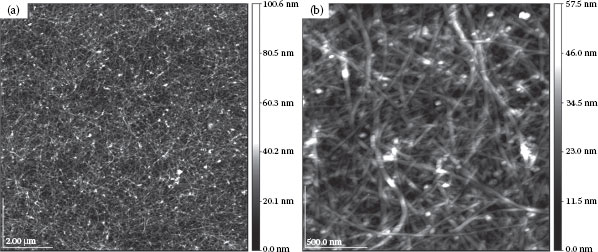
FIGURE 36.3 AFM images of a CNT film scanned over a large area of 10 × 10 μm2 (a) as well as a zoom-in of a smaller area of 2 × 2 μm2 (b). The values measured for the average and RMS surface roughness are 5.79 and 7.41 nm, respectively. (A. Abdellah et al., IEEE-NANO 2011, 11th IEEE Conference on Nanotechnology 2011, Portland, OR, pp.1118–1123. © (2011) IEEE. With permission.)
For certain applications of CNT films, evaluation of the electrical properties solely is not sufficient. The optical characterization of fabricated films can give insight into the influence and degree of doping/dedoping through chemical and thermal treatments. This can be achieved by the examination of metallic and semiconducting transitions in the absorption spectrum of films processed differently, as discussed previously. Moreover, in applications requiring optically transparent CNT films, the transmittance in the visible spectral range is of special interest. For this purpose, the transmittance at a wavelength of 550 nm is typically used as a representative value for comparison. As the optical losses increase naturally with increasing film thickness while the electrical losses decrease, a trade-off must be found for applications requiring both transparency and conductivity. Hence, a common approach for the evaluation of the electro-optical performance of such films is to plot sheet resistance as a function of the transmittance at 550 nm. This relation is plotted in Figure 36.5 for the fabricated CNT films. A good trade-off between sheet resistance and transmittance is achieved with films having 200 Ω/sq at 80% or 105 Ω/sq at 65% transmittance. These values closely match the state-of-the-art performance of films fabricated using more common and wellestablished deposition methods, such as spin coating or even vacuum filtration. Another method to quantify and compare transparent conductive thin films is by using the formula defined in Equation 36.1, where σop is the optical conductivity and Z0 = 377 Ω is the impedance of free space [15].
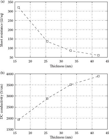
FIGURE 36.4 (a) Relation between sheet resistance (Rsh), as determined by four-point probe measurements, and film thickness. (b) The calculated values of DC conductivity (σdc) as a function of film thickness. (A. Abdellah et al., IEEE-NANO 2011, 11th IEEE Conference on Nanotechnology 2011, Portland, OR, pp.1118–1123. © (2011) IEEE. With permission.)
(36.1) |
This formula is originally applied to characterize thin metal films, where the absorption of the material is significantly lower than the reflectance and the thickness of the film is much smaller than the wavelength of interest. Typically, the value for the optical conductivity of CNT films at 550 nm is chosen to be 200 S/cm, as determined by Ruzicka et al. [16]. Since optical conductivity is independent of the doping levels, this value is assumed to be constant even among differently processed films. By fitting the data plotted in Figure 36.5 to this formula, a value of 7.5 is obtained for the ratio γ = σdc/σop, which is often used as a figure for a quantitative comparison of CNT thin-film performance. This figure should however be considered with caution and may not be suitable for straightforward comparison, since sheet resistance also depends on the type of SWNTs used and the level of doping. Tube diameter, average bundle length, and film roughness are detrimental factors for transmittance as well. The DC to optical conductivity ratio (γ), extracted from the relation between sheet resistance and transmittance, is therefore best suitable for the comparison of different films prepared using the same method and under similar conditions. Nevertheless, the values determined above are comparable to those reported for CNT films incorporating the same type of nanotubes (P3-SWNT, Carbon Solutions Inc), although they are fabricated using a different method [17].
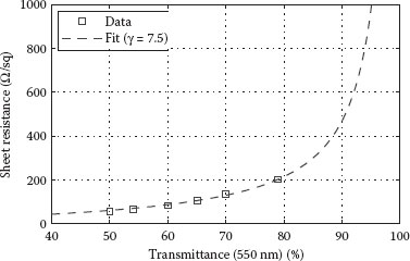
FIGURE 36.5 Plot of sheet resistance (Rsh) as a function of optical transmittance at 550 nm. A good trade-off between sheet resistance and transmittance is achieved with films having 200 Ω/sq at 80% or 105 Ω/sq at 65% transmittance.
All the figures discussed above demonstrate that the readily scalable air-atomizing spray deposition process presented here yields high-quality CNT thin films with a competitive electro-optical performance suitable for different device applications.
36.3.2 EFFECT OF PROCESS PARAMETER
The previous section was dedicated to a general description of the materials and methods involved in the CNT thin-film technology developed here. Note that a careful optimization of the different process parameters and processing conditions is crucial for achieving reliable and reproducible results using spray deposition. Several process-specific issues have to be addressed for the spray deposition and post-deposition treatment of CNT thin films based on different types of surfactants.
36.3.2.1 Sonication Time and CNT Distribution
The effect of sonication power and duration on the quality of the CNT dispersion used for nanotube deposition from a solution is of major significance for the performance of the resulting CNT thin film. It is necessary to differentiate between the different sources used for ultrasonic-assisted CNT dispersion into the solution. The two types typically used in such an application are bath and probe sonicators. While in a bath sonicator the ultrasonic power is generated in a water bath containing a flask with the CNT solution, a probe sonicator is directly immersed into the flask where the ultrasonic power is generated locally. This renders probe sonicators more powerful, hence requiring shorter sonication durations for solution preparation. The results discussed here to demonstrate the effect of sonication time on the characteristics of the final CNT film refer to the dispersions prepared by bath sonication. Figure 36.6 compares the relation between sheet resistance and transmittance for a variety of spray-deposited films from two CNT solutions prepared with different sonication durations. The data plotted show a clear shift toward higher values of sheet resistance at any given transmittance. Since excessive sonication introduces tube cutting and hence results in reduction of the average tube length [18], the electro-optical characteristics of the final CNT film suffer. This is a direct consequence of the percolation nature of such a CNT network, being composed of a random arrangement of particles with high-aspect ratios, where the percolation threshold scales inversely with the average tube length. A reduction of the average tube length therefore leads to an increase in the percolation threshold, with shorter sonication allowing for lower sheet resistance at a given optical transmittance or tube density [19].
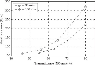
FIGURE 36.6 Variation of sheet resistance as a function of transmittance at 550 nm for SWNT films deposited from solutions with different sonication times. All films were chemically treated in concentrated HNO3 (65%) for 3 h following CMC removal.
To be able to evaluate the quality of a given CNT dispersion, an analysis of the CNT bundle distribution within the resulting film has to be performed. When considering films with very low CNT density or surface coverage, it is possible to extract information about the CNT length distribution by means of image processing. For this purpose, the CNT solution under investigation is highly diluted and used to spray a CNT network with ultra-low density onto a Si substrate. The sample is then processed further, according to the usual procedure, and its topography is characterized by AFM. Analysis of CNT bundles and their length distribution is finally performed using the image processing software ImageJ. Figure 36.7 shows the original AFM image obtained for such a sample along with the processed image used to generate the corresponding bundle length distribution. A histogram containing the bundle length distribution obtained for a sample sprayed with the CNT solution of 90 min sonication is plotted in Figure 36.8. A total of 79 CNTs are counted and considered in this distribution, hence allowing an acceptable statistical analysis. The histogram shows the relative frequency of occurrence for different tube lengths. It is then possible to fit the given tube length data with a log-normal distribution, as represented by the solid red line in the same figure. This is in good agreement with the CNT length distributions typically found in the literature [3]. For our film, the best fit is obtained using a log-normal distribution with a mean of 744 nm and a standard deviation of 95 nm. Longer SWNT bundles result in lower sheet resistances, due to less intertube junctions, which prevail in determining the overall film conductivity.
36.3.2.2 Chemical Treatment with Concentrated HNO3
Chemical post-deposition treatment with dilute HNO3 is needed for surfactant (CMC) removal as described above. At the same time, however, this treatment introduces an intentional p-type doping of the SWNT film. Treatment with concentrated HNO3 is found to be effective when a strong doping of the film is desired. We analyzed the reduction in sheet resistance of SWNT films with different thicknesses due to concentrated HNO3 (65%) treatment. The different samples were directly immersed into the HNO3 and the sheet resistance was recorded for varying treatment intervals. A graph containing the collected data is shown in Figure 36.9a. It is found that treatment with concentrated HNO3 for 1 h seems to be sufficient to approach the lowest value of sheet resistance for any given film, after which only slight reduction is observed. For all films within the thickness range examined here, a stabilization of sheet resistance occurs within 3 h of treatment. Moreover, the absolute change in sheet resistance for thinner films is larger than for thicker films. This is assumed to be due to the fact that thicker films, that is, ones with a higher tube density, contain a larger number of metallic tubes and hence more metallic paths, suppressing the effect of doping on the conductivity of semiconducting tubes. The relative change in sheet resistance is however similar for all samples, with a reduction by factors of 1.3–1.5 after treatment.
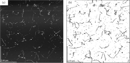
FIGURE 36.7 (a) AFM image of a CNT film with an extremely low tube density scanned over an area of 20 × 20 μm2. (b) The processed image used for bundle length analysis.
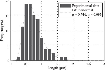
FIGURE 36.8 Histogram showing the relative frequency of occurrence for different tube lengths. It is possible to fit the given tube length data with a log-normal distribution with a mean of μ = 744 nm and a standard deviation of σ = 95 nm. (A. Abdellah et al., IEEE-NANO 2011, 11th IEEE Conference on Nanotechnology 2011, Portland, OR, pp.1118–1123. © (2011) IEEE. With permission.)
36.3.2.3 Optical Characteristics
In a discussion about the optical properties of CNT thin films, optical transmittance is of particular interest for organic optoelectronic device applications. As semitransparent electrodes in OLEDs or OPDs, an optimum of sheet resistance and transmittance within the visible range of the optical spectrum has to be carefully determined. Additionally, fundamental information on specific properties of the nanotubes incorporated in a film, such as electronic transitions and doping of nanotubes, can be obtained by the analysis of a broader spectral range extending beyond the visible wavelengths.
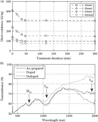
FIGURE 36.9 (a) Variation of sheet resistance as a function of concentrated HNO3 (65%) treatment duration for four films of different thicknesses. All films were previously subject to identical treatment in dilute HNO3 (13–23%) for CMC removal. (b) Optical transmittance spectra of an as-prepared, doped, and dedoped SWNT film.
The measured optical transmittance decreases with increasing CNT film thickness and is wavelength dependent. It is therefore necessary to define a representative value for the transmittance of any given CNT thin film. While in some cases this measure is defined as the average transmittance over a certain spectral range, usually including the visible and infrared range (400–1800 nm) [3], a more common convention is to use the transmittance at a fixed wavelength of 550 nm as a representative value. The latter yields moderate values and results in more realistic figures within the context of optoelectronic applications operated in the visible spectral range. Note that this figure can be considered to represent a lower limit, since film transmittance increases considerably in the infrared range. Depending on the application under development, a trade-off between optical and electrical losses must be found so as to fulfill the specifications required.
The characteristic absorption peaks attributed to electronic transitions at van Hove singularities can be observed in the optical transmittance spectrum of SWNT thin films, thereby deducing information about the extent of doping/dedoping through chemical and thermal treatments. To demonstrate this, an SWNT film was fabricated by spray deposition, which was then characterized once as-prepared and again after performing different post-deposition treatments. Figure 36.9b shows the wavelength-dependent optical transmittance curve of the as-prepared, spray-deposited film, where the different transitions are evident as absorption peaks. Interband energy transitions in semiconducting SWNTs are designated by S11 and S22 while the transition in metallic SWNTs is designated by M11, as typically found in the literature [20]. As photons are dependent on SWNTs, peak absorption occurs between energies with local maxima of electron density (van Hove singularities). Owing to p-type doping, electrons in the valence band are withdrawn and therefore no longer contribute to interband energy transitions. The withdrawal of electrons can be equivalently viewed as the injection of holes. Effects of p-type doping through chemical treatment of the same SWNT film by concentrated HNO3 (65%) can be seen in Figure 36.9b (doped). A nearly complete bleaching of the S11 transition and significant reduction of the S22 transition can be observed for the doped film. The preceding observation clearly confirms the occurrence of electron withdrawal from the valance band of the semiconducting SWNTs upon doping with HNO3. A similar effect is observed when films are chemically treated with SOCl2. The p-type doping of SWNTs can be reversed by a thermal treatment. Here, the film is annealed on a hot plate at 200°C for 2 h under ambient conditions. A substantial increase of the absorption peak corresponding to the S11 energy transition is observed, as seen in the transmittance curve (dedoped) shown in Figure 36.9b. Owing to the partial removal of the previously adsorbed oxygen species after thermal annealing of the film, electrons are returned to their initial state in the first van Hove singularity. Consequently, photon energies equal to the S11 electronic interband transition are absorbed as indicated by a dip in the transmittance curve located at a wavelength of approx. 1900 nm. The return of electrons to the p-type nanotubes causes a reduction in the excess charge carriers, which in turn leads to a reduction of the overall film conductivity. Sheet resistance is hence decreased from 100 Ω/sq for the HNO3 doped film to 420 Ω/sq by thermally induced dedoping. From the preceding example, we conclude that a qualitative evaluation of the extent of film doping is possible by a simple analysis of the optical absorption spectrum in the near-infrared range.
36.3.3 CNT NETWORKS FOR GAS SENSING
The inherently high surface-to-volume ratio of CNTs makes them an ideal candidate for environmental gas-sensing applications [6,7,21, 22, 23 and 24]. A common implementation for CNT gas sensors consists of an interdigitated electrode structure (IDES) forming the two contact terminals of the simple resistive architecture, above or beneath which a uniformly distributed resistive random network of CNTs is deposited. It is worth mentioning that the CNT film incorporated in our gas sensors has a significantly lower density/thickness than the films introduced above. The utilization of low-density films leads to better sensor response and higher sensitivities. This is considered to be a consequence of the more direct exposure of a greater portion of CNTs contributing to current conduction through the film, thereby enhancing the change of the overall film conductance when exposed to a given concentration of the test gas. A sensor readout is performed by applying a sensing current and measuring the voltage drop across the two terminals of the device, thus monitoring the relative change in resistance/onductance with respect to different controlled environmental conditions. Before sensor response toward the test gas is evaluated, the initial resistance of the network is monitored for a specified time in order to determine a baseline for the device under test. Baseline characterization was performed with a sensing current of 10 μA under a constant carrier (N2) gas flux of 200 mL/min at room temperature. A continuous increase in the resistance of the network can be observed during the first hour before a stable state is approached. In our opinion, this effect is attributed to a continuation of the dedoping process due to the flow of a relatively high-current density through the network. After reaching a stable initial resistance, the sensor response is investigated by exposing the sensor module inside a gas chamber to different concentrations of ammonia. The main figure used for the evaluation of sensor performance is the sensitivity, defined in Equation 36.2 as the relative change in resistance, where Ri and Rf are the initial and final resistance values of an exposure cycle, respectively.
(36.2) |
Figure 36.10a depicts the measured sensor resistance over time. The graph is divided into four segments, based on four exposure/recovery cycles at different NH3 concentrations of 10, 25, 50, and 100 ppm. Each cycle is composed of an exposure interval followed by a recovery interval. During exposure, NH3 is allowed to enter the chamber along with the carrier gas at room temperature and a constant flux of 200 mL/min for a 100 s time interval. Recovery is then introduced by heating the sensor module to 80°C and increasing the N2 flux to 1000 mL/min for 300 s, after which heating is stopped again. The high flux is maintained for another 300 s to accelerate cooling of the sensor and to purge any residual test gas molecules out of the chamber. Recovery is then completed by a final 300 s interval under sensing conditions to restore the initial resistance. The increase in thermal energy during the heating cycle is necessary to enhance desorption of gas molecules attached to the CNT film and to enable a complete recovery. One of the most prominent features observed in the response is the clear and immediate change in resistance at the start and end of NH3 exposure. Taking a look at the magnitude of change in resistance after exposure to different concentration reveals a clear increase in sensitivity with increasing concentration, at least up to a concentration of 100 ppm. This becomes more evident when displaying the sensitivity as a function of NH3 concentration, as plotted in Figure 36.10b. To avoid inaccuracies in sensitivity calculations due to delays in the gas system, Ri is recorded at the instance of abrupt change in resistance and Rf is defined as the resistance of the network 60 s later. This means that the sensitivities presented here correspond to an exposure interval of 60 s, which is to our knowledge shorter than the usual exposure intervals reported in the literature. Sensitivity is found to have a logarithmic dependence on the concentration, with sensitivities of 1% for concentrations as low as 10 ppm and reaching 5% at a concentration of 100 ppm. We consider these values for sensitivity to be very competitive taking into account the short exposure intervals of 60 s [8]. The response of the same sensor with passive recovery, that is, no heating or increased flux is applied during the recovery interval, is also shown in Figure 36.10b. It can be seen that the sensitivity is significantly lower due to incomplete recovery of the CNT film. Active recovery can therefore enhance sensitivity by a factor of 2, using the same sensor architecture in addition to a simple heating element.
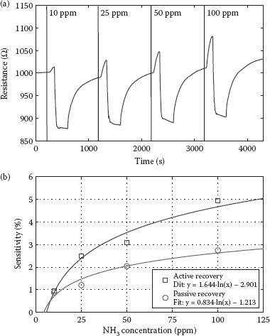
FIGURE 36.10 (a) Measured sensor resistance over time. The graph is divided into four segments, based on four exposure/recovery cycles at different NH3 concentrations of 10, 25, 50, and 100 ppm. (b) Plot displaying the sensitivity as a function of NH3 concentration. Sensitivities presented here correspond to the relative resistance changes in an exposure interval as short as 60 s with values reaching 5% at a concentration of 100 ppm. (A. Abdellah et al., IEEE-NANO 2011, 11th IEEE Conference on Nanotechnology 2011, Portland, OR, pp. 1118–1123. © (2011) IEEE. With permission.)
In conclusion, we presented a reliable and reproducible spray deposition process for the fabrication of highly uniform CNT films exhibiting a state-of-the-art performance. The convenient control of major process parameters enables a fine and accurate tuning of film characteristics. Average surface roughness was shown to be 5.79 nm, measured over an area of 10 × 10 μm2. The calculated conductivities were shown to vary with film thickness due to the percolating nature of CNT films. Conductivity increases to 4000 S/cm at 45 nm and approaches saturation beyond this thickness. A good trade-off between sheet resistance and transmittance is achieved with the best films having 200 Ω/sq at 80%.
Further, we report the successful implementation of CNT-based gas sensors with exceptionally high sensitivities and a fast response to various test gases. Highly uniform CNT thin films, prepared using a reliable and reproducible, low-cost spray deposition process, are utilized as resistive networks for gas detection. The sensitivity toward NH3 is examined along with passive and active recovery routines. Sensors show a clear and immediate change in resistance as a response to test gas exposure. Sensitivities of 1% for concentrations as low as 10 ppm and reaching 5% at a concentration of 100 ppm can be achieved in case of NH3. We consider these values for NH3 sensitivity to be competitive, taking into account the short exposure intervals of 60 s considered in our sensitivity calculations.
1. D. Zhang et al., Transparent, conductive, and flexible carbon nanotube films and their application in organic light-emitting diodes, Nano Letters, 6(9), 1880–1886, 2006.
2. Y. -M. Chien, F. Lefevre, I. Shih, and R. Izquierdo, A solution processed top emission OLED with transparent carbon nanotube electrodes, Nanotechnology, 21(13), 134020, 2010.
3. R. C. Tenent et al., Ultrasmooth, large-area, high-uniformity, conductive transparent single-walledcarbon-nanotube films for photovoltaics produced by ultrasonic spraying, Advanced Materials, 21(31), 3210–3216, 2009.
4. M. Ha et al., Printed, sub-3V digital circuits on plastic from aqueous carbon nanotube inks, ACS Nano, 4(8), 4388–95, Aug. 2010.
5. C. Wang, J. Zhang, and C. Zhou, Macroelectronic integrated circuits using high-performance separated carbon Nanotube thin-film transistors, ACS Nano, 4(12), 7123–7132, Nov. 2010.
6. J. Li, Y. Lu, Q. Ye, M. Cinke, J. Han, and M. Meyyappan, Carbon nanotube sensors for gas and organic vapor detection, Nano Letters, 3(7), 929–933, Jul. 2003.
7. E. Bekyarova et al., Chemically functionalized single-walled carbon nanotubes as ammonia sensors, The Journal of Physical Chemistry B, 108(51), 19717–19720, Dec. 2004.
8. M. Penza, R. Rossi, M. Alvisi, G. Cassano, and E. Serra, Functional characterization of carbon nanotube networked films functionalized with tuned loading of Au nanoclusters for gas sensing applications, Sensors and Actuators B: Chemical, 140(1), 176–184, Jun. 2009.
9. S. Kim, J. Yim, X. Wang, D. D. C. Bradley, S. Lee, and J. C. DeMello, Spin- and spray-deposited single-walled carbon-nanotube electrodes for organic solar cells, Advanced Functional Materials, 20(14), 2310–2316, 2010.
10. A. Abdellah, D. Baierl, B. Fabel, P. Lugli, and G. Scarpa, Exploring spray technology for the fabrication of organic devices based on poly(3-hexylthiophene). IEEE-NANO 2009. 9th IEEE Conference on Nanotechnology, Genoa, pp. 831–934, 2009.
11. A. Abdellah, B. Fabel, P. Lugli, and G. Scarpa, Spray deposition of organic semiconducting thin-films: Towards the fabrication of arbitrary shaped organic electronic devices, Organic Electronics, 11(6), 1031–1038, Jun. 2010.
12. T. Takahashi, K. Tsunoda, H. Yajima, and T. Ishii, Dispersion and purification of single-wall carbon nanotubes using carboxymethylcellulose, Japanese Journal of Applied Physics, 43(6A), 3636–3639, Jun. 2004.
13. D. Hecht, L. Hu, and G. Grüner, Conductivity scaling with bundle length and diameter in single walled carbon nanotube networks, Applied Physics Letters, 89(13), 133112, Sep. 2006.
14. E. Bekyarova et al., Electronic properties of single-walled carbon nanotube networks, Journal of the American Chemical Society, 127(16), 5990–5995, Apr. 2005.
15. L. Hu, D. Hecht, and G. Grüner, Percolation in transparent and conducting carbon nanotube networks, Nano Lett, 4(12), 2513–2517, Dec. 2004.
16. B. Ruzicka and L. Degiorgi, Optical and dc conductivity study of potassium-doped single-walled carbon nanotube films, Physical Review B, 61(4), R2468–R2471, Jan. 2000.
17. Y. Zhou, L. Hu, and G. Grüner, A method of printing carbon nanotube thin films, Applied Physics Letters, 88(12), 123109, Mar. 2006.
18. M. F. Islam, E. Rojas, D. M. Bergey, A. T. Johnson, and A. G. Yodh, High weight fraction surfactant solubilization of single-wall carbon nanotubes in water, Nano Letters, 3(2), 269–273, Feb. 2003.
19. D. Simien, J. A. Fagan, W. Luo, J. F. Douglas, K. Migler, and J. Obrzut, Influence of nanotube length on the optical and conductivity properties of thin single-wall carbon nanotube networks, ACS Nano, 2(9), 1879–84, Sep. 2008.
20. S. Niyogi et al., Chemistry of single-walled carbon nanotubes, Accounts of Chemical Research, 35(12), 1105–13, Dec. 2002.
21. J. Kong et al., Nanotube molecular wires as chemical sensors, Science, 287(5453), 622–625, Jan. 2000.
22. O. K. Varghese, P. D. Kichambre, D. Gong, K. G. Ong, E. C. Dickey, and C. A. Grimes, Gas sensing characteristics of multi-wall carbon nanotubes, Sensors and Actuators B: Chemical, 81(1), 32–41, Dec. 2001.
23. Y. -T. Jang, S.-I. Moon, J.-H. Ahn, Y. -H. Lee, and B.-K. Ju, A simple approach in fabricating chemical sensor using laterally grown multi-walled carbon nanotubes, Sensors and Actuators B: Chemical, 99(1), 118–122, Apr. 2004.
24. M. Arab, F. Berger, F. Picaud, C. Ramseyer, J. Glory, and M. Maynelhermite, Direct growth of the multi-walled carbon nanotubes as a tool to detect ammonia at room temperature, Chemical Physics Letters, 433(1–3), 175–181, Dec. 2006.
25. A. Abdellah et al., IEEE-NANO 2011, 11th IEEE Conference on Nanotechnology, Portland, OR, pp. 1118–1123, 2011.