
CONTENTS
38.2.2 Band Gap with Defect and Temperature
38.2.3 Band Gap with Temperature
38.3.1 Band Gap with Temperature
Carbon nanotubes (CNTs) have attracted the most attention due to their extraordinary electrical, mechanical, and optical properties [1, 2 and 3]. In addition to the efforts of developing new electronic devices, direct bandgap one-dimensional (1D) nanostructures are playing an important role because of the desire to integrate both electronic and optoelectronic technologies on the same material [2]. For example, CNT field-effect transistors (CNTFETs) have generated considerable attention over the past few years because of their semiconductive properties and have reached a high level of performance [4, 3, 4, 5, 6 and 7]. Meanwhile, several major technology-related questions still need to be addressed. The research on temperature-dependent CNTFET model is not adequate; which is one of the critical and dominant factors on electronics device performance.
The role of temperature has been established in semiconductors as one factor affecting the band gap. In CNTFETs, temperature has been neglected due to its small contribution of affecting the band gap, at room temperature, as opposed to how temperature affects silicon base semiconductors as in Ref. [8]. A qualitative comparison of various energy band gap equations is taken to view the effects of temperature outside room temperature.
Three band gap equations are used in this research; one of them is dependent mainly on the diameter, another on temperature and defect, and the last one has the use of temperature with parameters depending on chirality as in Refs. [8, 9 and 10]. The three equations are derived from single-wall nanotubes (SWNTs) and applied to coaxial-type CNTFETs. However, the temperature in CNTFETs is said to be negligible and can be ignored as stated in Ref. [8]. Thus, an investigation on how the temperature would affect these devices is conducted by using different equations with a set of various parameters.
The implementation of the band gap equation is followed by using the ID equation derived from ballistic nanotransistors as in Ref. [11], and the I–V curves can be simulated by using the MATLAB source codes found in the simulation tool named FETToy available at Nanohub.org. Temperature is the main parameter that is varied during simulation. The chirality vector is chosen for the small band gap of CNTs, such as m − n = 3 reported in Ref. [10]. Results have been obtained solely from simulations. For the next phase, other parameters would be included such as how temperature affects the Fermi levels at the channel, charge density, valley degeneracy, electron concentration, quantum capacitance, and mobile charge. The final step would be to compare the analytical model with the experimental results of a CNTFET.
The theory behind CNTs begins with an understanding of graphene. That is because SWNTs are considered to be rolled up graphene sheets. To solve the band structure of the graphene π orbitals, the steps are taken from [8] where the first step is to solve the Schrödinger equation
(38.1) |
where H is defined as the Hamiltonian, Ψ is the wave function, and E is the energy of the electrons in the π orbitals. The final solution to the energy is shown as
(38.2) |
Equation 38.2 demonstrates the valence bonds of graphene using the negative sign, and the conduction band vice versa where γ0 is the tight-bonding integral. Using Equation 38.2 the density of states (DOS) can be found by differentiating it. For a detailed look into solving the Schrödinger equation, the reader is asked to refer to Ref. [12]. Finally, by using Equation 38.2, the band gap equation is shown as
(38.3) |
Equation 38.3 does not have temperature dependence as the next two band gap equations to be shown, but is good to analyze with others to show how much the energy band gap differs.
38.2.2 BAND GAP WITH DEFECT AND TEMPERATURE
As mentioned before, SWNTs are made up from rolled up sheets of graphene and different electrical properties can be achieved depending on their chiral vector described as
(38.4) |
where (m, n) are integers and (a1, a2). Thus, by using Equation 38.4 if m = 0, the SWNT is thought to be zigzag and if n = m, it is said to be armchair; otherwise it is simply called chiral.
The next band gap equation can be found in more detail in Ref. [9], but basically the band gap equation is found by using the ambipolar random telegraph signal. The SWNTs used in this reference have small band gaps, where (m, n) will be in accordance with m − n = 3. They define the ratio of defect emission and capture times as
(38.5) |
where g is the trap degeneracy, Et is the defect energy, Ef is the Fermi energy, and kBT is the thermal energy. By using Equation 38.5, the band gap equation is found as
(38.6) |
The temperature parameter in Equation 38.6 varied from 4.2 K up to 115 K from reviewing [9].
38.2.3 BAND GAP WITH TEMPERATURE
The last band gap equation comes from Ref. [10] and is a bit complicated compared to the other two. The main idea is that there are two parts of the band gap equation, which consists of harmonic and anharmonic parts. The harmonic portion comes from the ground-state geometry and the anharmonic part is from thermal expansion. Thus, the band gap equation can be shown as
(38.7) |
The temperature in Equation 38.7 is varied such that T < 400 K and the chirality of the SWNTs used must follow the form of
(38.8) |
(38.9) |
where Equation 38.9 is the diameter of the SWNT and must remain dimensionless. Equation 38.7 also has some parameters as functions which are
(38.10) |
(38.11) |
(38.12) |
(38.13) |
(38.14) |
(38.15) |
The remaining parameters for the previous set of equations are shown in Table 38.1.
TABLE 38.1
Parameters for Previous Equations
A |
9.45 × 10³ K |
−1.70 × 10⁻⁵ eV/K |
|
1.68 × 10⁻⁶ eV/K |
|
6.47 × 10⁻⁷ eV/K |
|
470 K |
|
1.06 × 10³ K |
|
−5.94 × 10⁻² K |
|
B |
−4.54 × 10⁻⁴ eV/K |
−2.68 × 10⁻³ eV/K |
|
−2.23 × 10⁻⁵ eV/K |
Source: From R. B. Capaz et al., Physics Review Letters, 94, 036801, 2005. With permission.
38.3.1 BAND GAP WITH TEMPERATURE
The band gap equations are varied in different ways since each has specific things to observe; but the main feature that is noticed in the research is the temperature. At first, the diameter in Equation 38.3 is varied from 0.8 to 3 nm. It is mentioned in Ref. [12] that the energy band gap from Equation 38.3 will vary from 0.2 to 0.9 eV. A MATLAB plot of Equation 38.3 is shown in Figure 38.1; note that this is the only equation without temperature and can be used to compare how much the others will vary.
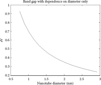
FIGURE 38.1 The diameter in Equation 38.3 is varied from 0.8 to 3 nm.
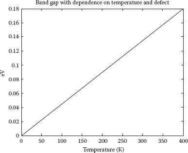
FIGURE 38.2 The band gap using Equation 38.6 behaves in a linear fashion with temperature.
Equation 38.6 shows a difference; there is no diameter parameter, but the measurements taken in Ref. [9] are done by having SWNTs in the range of 1–3 nm. The defect ratios are kept as (τe/τc)ne = 15 and (τe/τc)po = 12. The band gap using Equation 38.6 behaves in a linear fashion as shown in Figure 38.2.
Finally, the band gap equation used in Equation 38.7 is varied by temperature and is also shown with different diameter sizes of 1, 2.1, and 3 nm, as shown in Figure 38.3.
The band gap equations are simulated at temperatures of 50, 300, and 400 K with diameters of 1, 2.1, and 3 nm, respectively. The temperature-dependent energy band gap values are listed in Table 38.2. As it is shown, the energy band gaps vary tremendously depending on some critical parameters such as temperature, diameter, defect ratio, and so on.
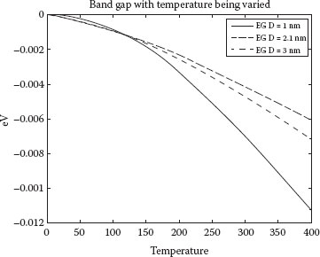
FIGURE 38.3 Temperature dependent band-gap behavior using the Equation 38.7
TABLE 38.2
Band Gaps at Different Diameters and Temperatures
Equation |
50 K |
300 Kp |
400 K |
Diameter = 1 nm |
|||
(38.3) |
0.8317 |
0.8317 |
0.8317 |
(38.6) |
0.02238 |
0.1343 |
0.1791 |
(38.7) |
−0.00236 |
−0.007038 |
−0.01128 |
Diameter = 2.1 nm |
|||
(38.3) |
0.4045 |
0.4045 |
0.4045 |
(38.6) |
0.02238 |
0.1343 |
0.1791 |
(38.7) |
−0.00039 |
−0.0004779 |
−0.00072 |
Diameter = 3 nm |
|||
(38.3) |
0.2789 |
0.2789 |
0.2789 |
(38.6) |
0.2238 |
0.1343 |
0.1791 |
(38.7) |
−0.00043 |
−0.0004287 |
−0.0061 |
The output I–V characteristics are also analyzed. The diameters used in the simulation are 1, 2.1, and 3 nm, respectively. The I–V characteristics are simulated at 50, 300, and 400 K. Figures 38.4 through 38.7 show the effects of temperature. The maximum current is affected as temperature increases, but the linear region seems not to be affected much by the temperature from Vds voltages of 0–0.2 V. It is also observed that the current of the CNTFET is a function of energy gap, diameter, defect of CNT, chiral vectors, chiral angel as well as temperature. It is observed from the figures that the drain current in the saturation region at higher temperatures is higher than at the lower temperature. However, for the lower drain–source voltages, the difference between the higher and lower temperature current regions remains almost constant.
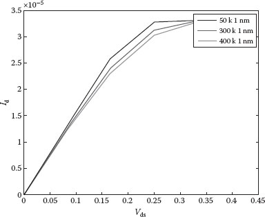
FIGURE 38.4 I–V curves at different temperatures.
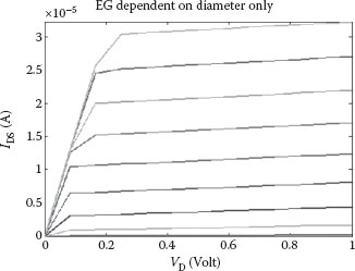
FIGURE 38.5 I–V using bandgap equation 38.3. Diameter 1 nm, temperature 50 K.
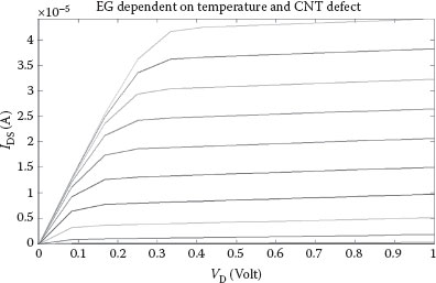
FIGURE 38.6 I–V using bandgap equation 38.6. Diameter 1 nm, temperature 300 K.
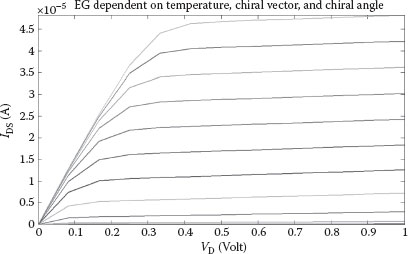
FIGURE 38.7 I–V using bandgap equation 38.7. Diameter 3 nm, temperature 400 K.
The research is specifically focused on the current–voltage characteristics of CNTFET considering the temperature variations. The results are in good accordance with their references. Temperature does show that it has some impact on the energy band gap and I–V characteristics. However, since each equation has specific variables, it is also important to note which parameters would be more important to go along with temperature. The effect of varying temperature on CNTFET also influences the on current, off current, on–off current ratio, transconductance, drain conductance characteristics, and the subthreshold swing.
Temperature definitely plays a significant role in the performance of all types of transistors. The need of CNTFET arises from the fact that most of the transistors design encounters a lot of problems during its operation in a very low-power supply [13,14]. Therefore, CNTFET can be a good solution, which provides more reliability even during aggressive scaling.
1. J. Guo, S. Goasguen, M. Lundstrom, and S. Datta, Metal–insulator–semiconductor electrostatics of carbon nanotubes. Applied Physics Letters, 81(8), 2002.
2. P. Avouris and J. Chen, Nanotube electronics and optoelectronics, Materials Today, 9(10), 46–54, 2006.
3. S. Iijima, Helical microtubules of graphitic carbon, Nature, 354(6348), 56–58, 1991.
4. S. J. Tans, A. R. M. Verschueren, and C. Dekker, Room-temperature transistor based on a single carbon nanotube, Nature, 393, 49–52, 1998.
5. R. Martel, T. Schmidt, H. R. Shea, T. Hertel, and P. Avouris, Single- and multi-wall carbon nanotube field-effect transistors, Appl. Phys. Lett., 73, 2447–2449, 1998.
6. J. J. Guo, D. B. Farmer, Q. Wang, E. Yenilmez, R. G. Gordon, M. Lundstrom, and H. J. Dai, Self-aligned ballistic molecular transistors and electrically parallel nanotube arrays, Nano Lett., 4, 1319–1322, 2004.
7. P. L. McEuen, M. S. Fuhrer, and H. Park, Single-walled carbon nanotube electronics, IEEE Transactions on Nanotechnology, 1(1), 78–85, 2002.
8. F. Leonard, The Physics of Carbon Nanotube Devices, 13 Eaton Ave. Norwich, NY 13815: William Andrew Inc., 2009, p. 20.
9. F. Liu, M. Bao, and K. L. Wang, Determination of the small band gap of carbon nanotubes using the ambipolar random telegraph signal, Nano Letters, 5(7), 1333–1336, 2005.
10. R. B. Capaz, C. D. Spataru, P. Tangney, M. L. Cohen, and S. G. Louie, Temperature dependence of the band gap of semiconducting carbon nanotubes, Physics Review Letters, 94, 036801, 2005.
11. A. Rahman, J. Guo, and S. Datta, Theory of ballistic nanotransistors, IEEE Transactions on Electron Devices, 50(9), 1853–1864, 2003.
12. J. J. Kong, Carbon Nanotube Electronics, New York: Springer, 2009, p. 1–9
13. Q. Lu, D. Park, and A. Kalnitsky et al., Leakage current comparison between ultra-thin Ta2O5 films and conventional gate dielectrics, IEEE Electron Device Letters, 19(9), 341–342, 1998.
14. K. Natori, Ballistic metal-oxide-semiconductor field effect transistor, Journal of Applied Physics, 76(8), 4879–4890, 1994.