
CONTENTS
Thin-film transistors (TFTs) are one of the most promising practical applications of single-walled carbon nanotubes (SWNTs) due to their flexible filament-like structure and high carrier mobility [1]. For the fabrication of industrial electrical devices, it is an inevitable issue to utilize both p- and n-type transistors as basic components of the electrical circuits. Since oxygen and water molecules adsorbing on the surface of SWNTs are known to play a role as an electron acceptor against SWNTs, SWNTs–TFTs have p-type semiconducting features. To date, there are several reports on the fabrication of n-type SWNTs–TFTs by functionalizing the outside surface of SWNTs [2]. However, the operation of n-type SWNTs–TFTs is limited only under the specific condition and the fabrication of stable n-type SWNTs–TFTs under the various environmental conditions has not been realized.
Here, we report on the successful fabrication of very stable n-type SWNTs–TFTs by encapsulating Cs atoms in SWNTs with a plasma ion irradiation method [3, 5, 6, 7, 8, 9, 10 and 11]. Since the graphitic network of carbon cells protects the inside Cs atoms from other reactive molecules that exist outside SWNTs, the n-type features are found to be very stable even after soaking for a long time in water.
The Cs atom encapsulation is carried out by a plasma ion irradiation method. Cs+–e– plasmas are generated by a thermal contact ionization method (Figure 40.1a) [3, 5, 6, 7, 8 and 9]. The typical plasma parameters are measured by a Langmuir probe and can be estimated from this Ip–Vp curve as follows: electron density (ne) ≈ 109 cm−3, electron temperature (Te) ≈ 0.2 eV, and space potential (φs) ≈ − 3 V. SWNTs are deposited on a SiO2 (300 nm)/Si substrate. To promote the adsorption of SWNTs, the SiO2 substrate surface is functionalized by 3-aminopropyltriethoxysilane (APTES) prior to the SWNTs deposition [12]. The pairs of Au electrodes are fabricated by a conventional photolithography technique. SWNTs–TFTs are put on a SUS plate, which is inserted into the plasma region. After the Cs irradiation, Cs-irradiated SWNTs–TFTs are carefully rinsed by purified water to remove the Cs atoms adsorbing on the outside of the SWNTs. The transport properties of SWNTs–TFTs are measured by a vacuum probe station and semiconductor parameter analyzer under a field-effect transistor (FET) configuration. The structure of Cs-irradiated SWNTs is also observed by transmission electron microscopy (TEM).
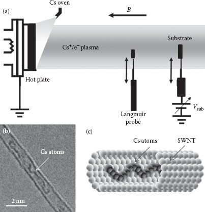
FIGURE 40.1 (a) Schematic illustration of Cs @ SWNTs formation process. (b, c) A typical TEM image and model of Cs @ SWNT.
Figures 40.1b and c show a typical TEM image and a model of Cs encapsulated (@) SWNTs. The one-dimensional chain-like structures of Cs atoms are often and clearly observed inside SWNTs by TEM observation. The typical source–drain current (Ids) versus gate bias voltage (Vgs) curves of the same device after the Cs plasma irradiation are investigated as a function of Cs irradiation time (Figure 40.2a). The source–drain voltage (Vds) is fixed at 1 V. The saturated source–drain current (Ids) ratio of n- to p-channel [(Ionn–Ioff)/(Ionp–Ioff)] is utilized as a guidepost to estimate the conducting type of SWNTs–TFTs (Figure 40.2b), where Ioff denotes the off current corresponding with the current from metallic SWNTs. The value of (Ionn–Ioff)/(Ionp–Ioff) clearly increases with an increase in the Cs irradiation time. A similar tendency is also observed from the plot of the threshold gate bias voltage (Vgth). Vgth shifts to the negative Vgs direction with an increase in the Cs irradiation time. This indicates that the electrical transport property of SWNTs–TFTs can be precisely controlled by tuning the doping density of Cs inside SWNTs.
To confirm the stability of Cs @ SWNTs–TFTs, the transistors are soaked in purified water for a certain period. Figure 40.3 gives the soaking time dependence of Ids–Vgs curves for Cs @ SWNTs–TFTs. Although the threshold of the gate bias voltage slightly shifts to the positive Vgs direction between 0 and 4 h soaking time, the change in the Ids–Vgs feature is almost saturated by 8 h. This indicates that Cs atoms adsorbing on the outside of SWNTs should be washed out during the 0–4 h. Since the Ids–Vgs does not show an obvious change after an 8 h soak and the n-type feature is maintained, the transition from a p- to an n-type property should originate from the encapsulated Cs atoms inside SWNTs, which remain very stable even under water.
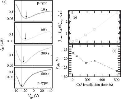
FIGURE 40.2 (a) Ids–Vgs curves of Cs @ SWNTs-TFTs for different Cs plasma irradiation times. (b) (Ionn–Ioff)/(Ionp–Ioff) and (c) Vgth plot as a function of Cs plasma irradiation time.
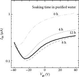
FIGURE 40.3 The soaking time dependence of Cs @ SWNTs-TFTs features in the purified water.
We have succeeded in fabricating very stable n-type SWNTs–TFTs with Cs@SWNTs and found that the transport property of SWNT–TFTs clearly changes from a p- to an n-type after Cs plasma irradiation. On the basis of systematic investigation, the n-type property is very stable under the long soak in water. These stable n-type SWNTs–TFTs are very important for the industrial fabrication of high-performance electrical circuits with SWNTs–TFTs.
This work was supported by a grant-in-aid for scientific research from the Ministry of Education, Culture, Sports, Science and Technology, Japan.
1. Q. Cao, H.-S. Kim, N. Pimparkar, J. P. Kulkarni, C. Wang, M. Shim, K. Roy, M. A. Alam, and J. A. Rogers, Medium-scale carbon nanotube thin-film integrated circuits on flexible plastic substrates, Nature, 454(7203), 495–500, 2008.
2. P. Qi, O. Vermesh, M. Grecu, A. Javey, Q. Wang, and H. Dai, Toward large arrays of multiplex functionalized carbon nanotube sensors for highly sensitive and selective molecular detection, Nano Letters, 3(3), 347–351, 2003.
3. T. Hirata, R. Hatakeyama, T. Mieno, and N. Sato, Production and control of K–C60 plasma for material processing, Journal of Vacuum Science Technology A, 14(2), 615–618, 1995.
4. G.-H. Jeong, T. Hirata, R. Hatakeyama, K. Tohji, and K. Motomiya, C60 encapsulation inside single-walled carbon nanotubes using alkali-fullerene plasma method, Carbon, 40(12), 2247–2253, 2002.
5. G.-H. Jeong, R. Hatakeyama, T. Hirata, K. Tohji, K. Motomiya, T. Yaguchi, and Y. Kawazoe, Formation and structural observation of cesium encapsulated single-walled carbon nanotubes, Chemical Communications, (1), 152–153, 2003.
6. G.-H. Jeong, A. A. Farajian, R. Hatakeyama, T. Hirata, T. Yaguchi, K. Tohji, H. Mizuseki, and Y. Kawazoe, Cesium encapsulation in single-walled carbon nanotubes via plasma ion irradiation: Application to junction formation and ab initio investigation, Physical Review B, 68(7), 075410-1-6, 2003.
7. T. Izumida, R. Hatakeyama, Y. Neo, H. Mimura, K. Omote, and Y. Kasama, Electronic transport properties of Cs-encapsulated single-walled carbon nanotubes created by plasma ion irradiation, Applied Physics Letters, 89(9), 093121-1-3, 2006.
8. Y. F. Li, R. Hatakeyama, T. Kaneko, T. Izumida, T. Okada, and T. Kato, Electronic transport properties of Cs-encapsulated double-walled carbon nanotubes, Applied Physics Letters, 89(9), 093110-1-3, 2006.
9. R. Hatakeyama and Y. F. Li, Synthesis and electronic-property control of Cs-encapsulated single- and double-walled carbon nanotubes by plasma ion irradiation, Journal of Applied Physics, 102(3), 034309-1-7, 2007.
10. T. Kato, R. Hatakeyama, J. Shishido, W. Oohara, and K. Tohji, p–n Junction with donor and acceptor encapsulated single-walled carbon nanotubes, Applied Physics Letters, 95(8), 083109-1-3, 2009.
11. Y. F. Li, R. Hatakeyama, W. Oohara, and T. Kaneko, Formation of p–n junction in double-walled carbon nanotubes based on heteromaterial encapsulation, Applied Physics Express, 2(9), 095005-1-3, 2009.
12. L. Zhang, S. Zaric, X. Tu, X. Wang, W. Zhao, and H. Dai, Assessment of chemically separated carbon nanotubes for nanoelectronics, Journal of the American Chemical Society, 130(8), 2686–2691, 2007.