
CONTENTS
41.3 Printing Fabrication Technology
41.3.1 Device Fabrication Flow
41.3.4 CNT Random Network Channel
41.4 Printed CNT Thin Film Transistors
Single-wall carbon nanotubes (CNTs) [1] have a large intrinsic mobility [2] and are expected to be useful as a new electronic material. However, their electronic structures depend on their diameters and chirality, where one-third of the pristine CNTs are metallic (m-) and the other two-thirds are semiconducting (s-) [3]; thus, they intrinsically contain metallic contamination. Therefore, it is crucial to mitigate the effect of m-CNTs when making use of CNTs as semiconducting materials. There are two approaches, increasing s-CNT purity and decreasing the influence of m-CNT. Using a CNT random network as a thin film transistor (TFT) channel [4] is one of the best ideas to prevent device shorts caused by m-CNTs. According to the simulation work, a CNT random network is tolerant to m-CNT contamination [5]. Furthermore, CNT random networks are compatible with solution processes such as s-CNT purification [6] and printing fabrication. The device yield and performance of a CNT random network TFT can be increased by the use of purified s-CNTs.
On the other hand, printed electronics enable large-area and flexible electronics on plastic substrates [7]. The key feature of print fabrication is simultaneous material deposition, and pattern definition by fully additive processes. This feature reduces the number of process steps and the amount of waste material during fabrication, and leads to low-cost and eco-friendly fabrication from a minimum of materials. Furthermore, maskless printing enables on-demand production by decreasing the lead time with offering flexibility in the circuit design. Therefore, printed electronics are attractive even though the resolution of the printing methods is three orders of magnitude larger than that of photolithography. Actually, it is difficult to fabricate high-density and high-functioning circuits by printing. Therefore, printed electronics are rather suited to implementing devices such as large-area sensing sheets, lightweight human interfaces, RF devices with multiple antennas, and so on. It is expected that such de novo electronics fields will be open by printed electronics.
The key issue is successful fabrication of printed TFTs in order to realize printed electronics, and the performance of the TFTs strongly affects the application field. The performance of printed TFTs is expected to increase by adopting CNT channels with high carrier mobility. A high-mobility TFT with a solution-processed CNT network was fabricated on an Si wafer [8]. It showed the excellent potential of a CNT network channel, but it was solid and its gate electrode was not individually fashioned. A flexible and high-mobility TFT was also fabricated on a polymeric substrate [9]; however, it required an additional patterning process for device separation. Inkjet printing is a promising candidate for the direct formation of a CNT network, but because the performance of the current TFTs does not appear competitive [10,11], technological development for printed CNT–TFTs is desired.
We developed a fabrication technology for printed CNT–TFTs. All electrodes, insulators, and CNT channels were directly printed without additional patterning processes. In this fabrication, surface-free energy was controlled for precise pattern definition. In addition, a mechanism for adsorbing CNTs was applied to channel formation in order to achieve homogeneous dispersion of the CNT random networks. We also developed an s-CNT purification method and fabricated the CNT–TFTs on the plastic films. The TFT characteristics clearly demonstrated the advantages of the purified s-CNT ink. The on-current of the printed CNT–TFT was increased without deterioration in the on/off ratio. A large field-effect mobility of 3.6 cm2/Vs was obtained for the printed CNT–TFTs with an on/off ratio of about 1000.
In this study, we used two types of CNT inks, CNT-1 and CNT-2. For CNT-1 preparation, commercially available CNTs (CoMoCAT SG65, Southwest Nano Technologies) were dispersed into a mixed organic solvent of xylene and dichloroethane by ultrasonication. CNT-1 has low surface tension and dries quickly on the substrates. It contains only volatile materials except for CNTs; however, it may contain about 33% m-CNTs. CNT-2 was an aqueous suspension and has higher surface tension than CNT-1. CNTs grown by chemical vapor deposition [12] were dispersed into heavy water (D2O) with polyoxyethylene alkyl ether, a nonionic surfactant, and s-CNT was purified by the electric-field-induced layer formation (ELF) method [13]. The micelles containing s-CNT were extracted to the anode region by applying a direct current (DC) electric field for a few tens of hours (Figure 41.1a). This extraction was repeated twice, and we estimated from the absorption spectra (Figure 41.1b) that the purity of s-CNT had increased more than 95%. According to thermogravimetric analysis (TGA), most parts of the surfactants can be removed by heat treatment at 180°C in air (Figure 41.2). Both types of CNT inks can be handled in ambient conditions.
41.3 PRINTING FABRICATION TECHNOLOGY
41.3.1 DEVICE FABRICATION FLOW
Device fabrication flow is shown in Figure 41.3. All device elements were patterned by maskless printing methods with a minimum of materials. First, gate electrodes were printed on a polyimide (PI) film by use of an inkjet printer with nano-Ag ink (NPS-J, Harima Chemicals) and sintered in air. Next, gate insulators were formed by an ink dispenser with PI ink (CT4112, Kyocera Chemical) and cured in an N2 oven. For some TFT samples, a 30-nm-thick SiO2 film was sputter deposited. This film was not for insulation but acted as a seed layer for a 3-aminopropyltriethoxysilane (APTES) monolayer, which was formed just before CNT channel formation. Then the source and drain electrodes were printed with nano-Ag ink and sintered. Finally, CNT ink was cast on the channel regions by a dispenser. When CNT-2 ink was used for the fabrication, the surfactants were removed from the channel regions by posttreatment with a combination of heat and wet processes. The maximum temperature was 200°C during the fabrication. In this study, we used a sputtered SiO2 layer as a seed for APTES modification. However, reliable insulation is not required for the layer, so it can be replaced by printable materials such as hydrogen silsesquioxane.
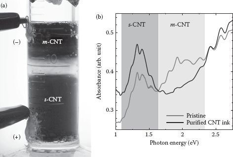
FIGURE 41.1 (a) s-CNT purification by the electric-field-induced layer formation (ELF) method [13]. (b) Absorption spectra of purified s-CNT ink and pristine CNT suspension. (H. Numata et al., Printing technology and advantage of purified semiconducting carbon nanotubes for thin film transistor fabrication on plastic films, Proc. Int. Conf. lEEE Nano 2011, Portland, OR, pp. 1000–1005. © (2011) IEEE. With permission.)
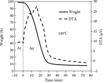
FIGURE 41.2 TGA chart of the surfactants used for CNT-2.
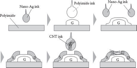
FIGURE 41.3 Print fabrication flow.
In this fabrication process, all device geometries were defined by printing methods without an additional patterning process. Therefore, it is important to control the wettability between the material inks and the underlying surfaces. In addition, there are two keys in the fabrication process. One is the reliability and uniformity of the printed gate insulators in order to successfully form such layered device structures. The other is the homogeneous dispersion of the CNT networks to improve device quality and performance. The details are described later.
Wetting tests were performed and surface free energy was quantitatively evaluated with Kaelble’s model [14], which provides dispersive and polar components of the surface free energy separately. The contact angles (θ) were measured with three probe liquids, water, methylene iodide, and formamide, whose polar and dispersive surface tension components are known. According to Kaelble’s model, the relation of the parameters is described as
(41.1) |
All measured data were plotted, and the surface free energy components and were estimated from the squares of the intercept and slope of the linear regression line, respectively (Figure 41.4a).
We used a corona discharge scanner to change the surface free energy because it enables simple and rapid treatment in the atmosphere. Figure 41.4b shows the surface energy of the PI film treated by the corona discharge method. In Figure 41.4b, the horizontal axis indicates the treatment time for a unit film length (the reciprocal of the scanning speed). The film had large and small before treatment. After treatment, decreased from the initial value, and increased with the treatment time. In Figure 41.4b, the total free energy represents the summation of and .
Figures 41.5a–c show the Ag dot patterns printed on the PI surfaces with various surface free energy components. The printed Ag dots were enlarged when and were 37.0 and 1.9 mJ/m2, respectively. This is a hydrophobic surface, and the dispersive component was too large to print fine nano-Ag patterns precisely (Figure 41.5a). The fine Ag dots were obtained when and were 24.3 and 18.8 mJ/m2, respectively (Figure 41.5b). It is interesting that the total surface energy was larger than in the former case. In the case of a rather hydrophilic surface, and were 28.1 and 34.7 mJ/m2, respectively; the printed Ag ink was spread on the surface; and the dots could not be separated (Figure 41.5c). Thus, it is very important to control the surface free energy for precise pattern definition in printing.
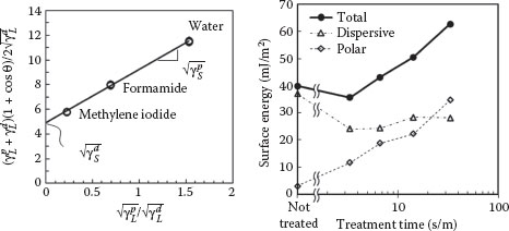
FIGURE 41.4 (a) Surface free energy estimation based on Kaelble’s model [14], and (b) estimated surface energy for the PI surface treated by the corona discharge method. (H. Numata et al., Printing technology and advantage of purified semiconducting carbon nanotubes for thin film transistor fabrication on plastic films, Proc. Int. Conf. lEEE Nano 2011, Portland, OR, pp.1000–1005. © (2011) IEEE. With permission.)
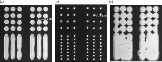
FIGURE 41.5 Ag dot patterns printed on the PI surfaces with various surface free energies. (a) mJ/m2 and mJ/m2, (b) mJ/m2 and mJ/m2, and (c) mJ/m2 and mJ/m2.
The electric properties of the insulators were evaluated to assess the printed Ag/PI/Ag stacked structures. The thickness of the printed films was controlled by surface free energy and printing conditions such as ink volume and solute concentration. Figures 41.6a and b show the current–voltage (I–V) and capacitance–voltage (C–V) characteristics for the printed PI layers whose thickness was about 600 nm. The printed Ag electrodes have much rougher surfaces because the grains grow up to about 100 nm during sintering. However, the printed PI layers have very small leakage currents for a 40 V bias (Figure 41.6a). The capacitances were independent of the bias, and the thickness of the printed PI was estimated from the capacitance value. A relative dielectric constant (kGI) of 2.59 was estimated in advance from reference samples, which had a 500-nm-thick, spin-coated PI layer sandwiched between the upper and lower Au electrodes, which were deposited by E-gun evaporation. In Figure 41.7, the horizontal and vertical axes show the estimated thickness and the normalized conductance at 1 MHz. We evaluated 91 samples, and an average thickness (tGI) of 630 nm with a standard deviation (σ) of 4.9% was obtained. Consequently, reliable and uniform printed insulators were obtained.
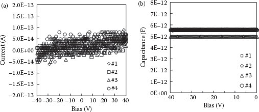
FIGURE 41.6 (a) I–V characteristics, and (b) C–V characteristics of the printed PI films.
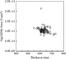
FIGURE 41.7 Estimated thickness and normalized conductance of the printed PI films at 1 MHz.
41.3.4 CNT RANDOM NETWORK CHANNEL
Homogeneous dispersion is required for a CNT network because aggregation and bundles emphasize the effect of m-CNTs on the device characteristics. CNT-1 ink has small surface tension and dries rapidly. Thus, it is expected that the droplet spreads out immediately and is parched before aggregation on the solid surface. However, it is difficult to precisely control the size of the channel regions because the droplet edge is dynamic. CNT-2 ink has a larger surface tension and its droplet is relatively stable. In this case, CNTs tend to be deposited at the edge of the droplet and form a ring-shaped condensed region. It is a well-known phenomenon, the so-called “coffee stain.” In the drying droplet, the contact line is pinned, and the evaporating solvent from the edge is replenished from the interior; consequently, an outward capillary flow occurs and carries the solute to the edge [15]. In such a condensed region, the m-CNT density would exceed the percolation threshold [16] locally and result in leakage current. To prevent “coffee stain” formation at the edge, CNTs need to be actively deposited in the middle of the droplet against the outward flow. Thus, a mechanism to adsorb CNTs should be appended to the surface to be printed.
Many surface treatment methods were investigated for effective CNT adsorption. An APTESmodified SiO2 surface provided an excellent result. An amino-silanized SiO2 surface was used to adsorb CNTs surrounded by ionic surfactants of sodium dodecylsulfate (SDS) [17]. An APTES-modified surface was also used for the suspensions of CNTs in amide solvents [18]. We carried out an adsorption test with an organic CNT suspension that was similar to CNT-1 ink. Although no surfactant was used, a high boiling solvent mixture of dodecane and triglyme (triethylenglykol-dimethylether) was used. A puddle of the suspension was formed on the surface for 60 min and blown away by N2 gas. CNTs adsorbed on the surface were observed with an atomic force microscope (AFM). Figures 41.8a–c indicate AFM images of the CNT adsorption test. A few CNTs were observed on the bare SiO2 surface (Figure 41.8b). On the APTES-modified SiO2 surface, many CNTs were adsorbed uniformly (Figure 41.8b). Conversely, they were rarely adsorbed on the hexamethyldisilazane (HMDS)-modified SiO2 surface (Figure 41.8c). The APTES and HMDS functionalize the SiO2 surface with the amino and methyl groups, respectively. It was confirmed that CNTs are effectively adsorbed by the amino groups. It was also confirmed that the APTES-modified SiO2 surface actively adsorbed the micelles containing s-CNT in CNT-2 ink [19]. The APTES layer chemically couples with the SiO2 surface, so a 30-nm-thick sputtered SiO2 layer was used as a seed layer in the device fabrication. The layer can be replaced by printable materials such as hydrogen silsesquioxane because reliable insulation is not required.
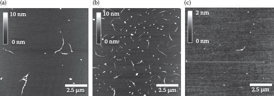
FIGURE 41.8 Results of the adsorption test for CNT ink. AFM height images of the CNTs on a (a) bare SiO2 surface, (b) APTES-modified SiO2 surface, and (c) HMDS-modified SiO2 surface.
41.4 PRINTED CNT THIN FILM TRANSISTORS
A 10 × 10 TFT array was printed on a 48.7 mm × 42.3 mm PI film substrate (Figure 41.9a). The fabrication conditions were determined by a combination of two types of CNT inks and three types of surfaces on which the CNT channels were printed. The fabricated samples are listed in Table 41.1 with symbols used in the following figures. The open and gray-colored symbols correspond to the samples with CNT-1 and -2 inks, respectively. The symbol shapes of circles, diamonds, and triangles correspond to the surfaces of CT4112, bare SiO2, and APTES-modified SiO2, respectively. Each sample has 100 TFTs, and the amount of CNT ink was varied in the samples. A small droplet of 10–20 nL CNT ink was cast 1–16 times to form a TFT channel. In Table 41.1, the square symbols represent the additional samples. Sample 4 was fabricated under conditions similar to those of sample 1, but the “excessive shots” were further cast to the CNT channel. Sample 8 had conditions similar to those of sample 7, but “posttreatment” to remove surfactants from the CNT network was different. Figure 41.9b represents the micrograph of a printed CNT–TFT immediately after a droplet of CNT-2 ink was cast between the source and drain electrodes. The channel width (W) and length (L) were about 610 and 100 μm, respectively.
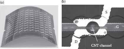
FIGURE 41.9 (a) Fabricated 10 × 10 array sample, and (b) micrograph of a printed CNT–TFT on a plastic film. (H. Numata et al., Printing technology and advantage of purified semiconducting carbon nanotubes for thin film transistor fabrication on plastic films, Proc. Int. Conf. lEEE Nano 2011, Portland, OR, pp. 1000–1005. © (2011) IEEE. With permission.)
No. |
CNT link |
Surface |
Symbol |
Remarks |
1 |
CNT-1 |
CT4112 |
|
|
2 |
CNT-1 |
SiO2 |
|
|
3 |
CNT-1 |
APTES |
|
|
4 |
CNT-1 |
CT4112 |
|
Excessive shots |
5 |
CNT-2 |
CT4112 |
|
|
6 |
CNT-2 |
SiO2 |
|
|
7 |
CNT-2 |
APTES |
|
|
8 |
CNT-2 |
APTES |
|
Post-treatment |
Figure 41.10 shows typical transfer characteristics of CNT–TFTs with a gate voltage that varied from −20 to 20 V at a drain voltage (VD) of −2 V. They indicate p-type characteristics and their on/off ratio was greater than 10,000. The printed CNT–TFTs had excellent quality. The relationship between on-current (Ion) and on/off ratio for all devices was studied (Figure 41.11). In Figure 41.11, there are four trend curves, (i)–(iv). Curve (i) corresponds to TFTs with low on/off ratios. For curves (ii) and (iii), the maximum on/off ratio exceeded 10,000. However, there was a trade-off between Ion and the on/off ratios observed in higher Ion regions. The critical values of Ion for which the on/off ratio decreased drastically were different for curves (ii) and (iii). Curve (iv) is a group of TFTs that has a large Ion with a rather high on/off ratio.
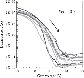
FIGURE 41.10 Transfer characteristics of printed CNT–TFTs. (H. Numata et al., Printing technology and advantage of purified semiconducting carbon nanotubes for thin film transistor fabrication on plastic films, Proc. Int. Conf. lEEE Nano 2011, Portland, OR, pp. 1000–1005. © (2011) IEEE. With permission.)
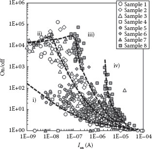
FIGURE 41.11 Ion dependence of on/off ratio for printed CNT–TFTs. (H. Numata et al., Printing technology and advantage of purified semiconducting carbon nanotubes for thin film transistor fabrication on plastic films, Proc. Int. Conf. lEEE Nano 2011, Portland, OR, pp. 1000–1005. © (2011) IEEE. With permission.)
The Ion dependence of the off-current (Ioff) is also plotted in Figure 41.12 in order to understand the deterioration in the on/off ratio in the high Ion region. For the CNT random network TFTs, Ion represents the total number of CNTs in the channel, and Ioff is strongly affected by m-CNTs because all of the current paths consist only of m-CNTs.
Curve (i) mainly consists of TFTs of samples 4 and 5, and the TFTs have large values of Ioff even in the small Ion region. When Ion increases, Ioff also increases, and the on/off ratio approaches 1. In the preliminary experiments for sample 4, when excessive shots were cast into the CNT channel, the cast ink washed away the formerly deposited CNTs in the channel and a ripple-like aggregation was formed (Figure 41.13a). For sample 5, stable droplets of CNT ink were formed and the surface had no mechanism for the adsorption of CNTs. Therefore, CNTs tended to aggregate like “coffee stains” as shown in Figure 41.13b. For both samples, it is conceived that stripes of CNT aggregations formed across the channel area. In such aggregations, the density of m-CNT exceeds the percolation threshold locally and caused large values of Ioff, even in the small Ion region.
Curves (ii) and (iii) consist of TFTs with CNT-1 and -2 inks, respectively. In the small Ion region, the values of Ioff were very small and the on/off ratios were approximately 10,000. As Ion increased, Ioff increased, and each curve has a critical value of Ion for which Ioff increased drastically. It is thought that the m-CNT density exceeded the percolation threshold and the leakage current increased above the critical Ion. The critical Ion values are about 3 × 10⁻⁸ A and 2 × 10⁻⁷ A for curves (ii) and (iii), respectively. The difference between them clearly shows the advantage of employing s-CNT purification for CNT-2. CNT-2 ink contains an order of magnitude fewer m-CNTs than CNT-1 ink. Therefore, the critical Ion for the TFTs with CNT-2 ink increased than that for the TFTs with CNT-1 ink by up to an order of magnitude. The Ion values increased without deterioration in device quality for the printed CNT–TFT by adopting purified s-CNT ink.
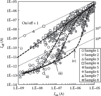
FIGURE 41.12 Ion dependence of Ioff for printed CNT–TFTs. (H. Numata et al., Printing technology and advantage of purified semiconducting carbon nanotubes for thin film transistor fabrication on plastic films, Proc. Int. Conf. lEEE Nano 2011, Portland, OR, pp. 1000–1005. © (2011) IEEE. With permission.)
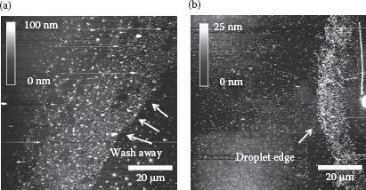
FIGURE 41.13 Results of the morphology test in the preliminary experiments. (a) When excessive shots were cast into the CNT channel, the cast ink washed away the formerly deposited CNTs. (b) “Coffee stains” appeared when a stable droplet was formed and the surface had no mechanism to adsorb CNTs.
In curve (iv), large Ion TFTs with a rather high on/off ratio were obtained. We used a simple parallel plate model for the gate capacitance and calculated field-effect mobility (μ) using the formula
(41.2) |
where L is the channel length, W is the channel width, tGI is the gate insulator thickness, kGI is the relative dielectric constant of the gate insulator, VD is the drain voltage, and dID/dVG is the mutual conductance estimated from the transfer characteristics. The relationship between fieldeffect mobility and on/off ratio for printed CNT–TFTs was plotted in Figure 41.14. In curve (iv), we obtained a CNT–TFT that has a high mobility of 3.6 cm2/Vs with an on/off ratio of about 1,000.
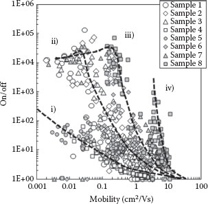
FIGURE 41.14 Relationship between field-effect mobility and on/off ratio for printed CNT–TFTs.
Curve (iv) consists of a part of the TFTs in sample 8. Sample 8 was fabricated with CNT-2 ink and APTES-modified SiO2. Figure 41.15 indicates the AFM phase image of the CNT channel in sample 8. The CNTs are indicated as dark and narrow lines. A dense and uniform CNT random network was observed. Therefore, we can obtain a large Ion for TFTs with a rather high on/off ratio. The TFTs of sample 8 belong to curves (iii) and (iv). On the contrary, sample 7 has no TFTs belonging to curve (iv). Samples 7 and 8 were fabricated under the same conditions, except for the posttreatment to remove the surfactants from the channels. Sample 7 was baked first and then wet processed. Sample 8 was soaked in isopropyl alcohol and rinsed with deionized water before heat treatment. In the preliminary experiment, we found that the CNTs aggregated slightly when the device was soaked in a liquid before heat treatment. It is thought that the micelles migrated and reconstructed on the surface in the liquid environment. Consequently, the CNT morphology was modified by the posttreatment. It is expected that the slight aggregation decreased the CNT–CNT contact resistance and increased the mobility for curve (iv). It was also reported that the Y-type junctions had low contact resistance between the CNTs, and it led to increased mobility of CNT–TFTs [20].
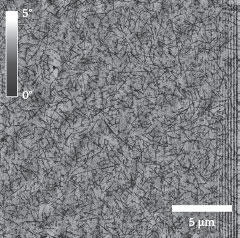
FIGURE 41.15 AFM phase image of printed CNT channel in sample 8.
A fabrication technology for printed CNT–TFTs was developed. All electrodes, insulators, and CNT channels were directly patterned without additional patterning processes such as photolithography and etching. In the fabrication process, surface free energy was controlled for precise pattern definition. In addition, a mechanism for adsorbing CNTs was applied to channel formation in order to achieve homogeneous dispersion of the CNT random networks. The CNT–TFTs were fabricated on the plastic films with a minimum of materials. A purified s-CNT ink was used, and its advantage was clearly demonstrated by the TFT characteristics. The on-current of the printed CNT–TFT increased without deterioration in the on/off ratio. A high mobility of 3.6 cm2/Vs was obtained with an on/off ratio of about 1000. In addition, we successfully fabricated high-uniformity printed CNT–TFTs recently with a σ of 30% by use of this print fabrication technology. The drain current distributions for the on- and off-states were entirely separated, and this result indicates that the printed CNT–TFTs are capable of select switching in a two-dimensional matrix [19]. These results are definitely promising for the realization of printed electronics integrated with CNT–TFTs.
The authors would like to thank Shinichi Yorozu and Hiroyuki Endoh for their helpful discussions. A part of this work was supported by New Energy and Industrial Technology Development Organization (NEDO).
1. S. Iijima and T. Ichihashi, Single-shell carbon nanotubes of 1-nm diameter, Nature, 363, 603–605, 1993.
2. T. Dürkop, S. A. Getty, E. Cobas, and M. S. Fuhrer, Extraordinary mobility in semiconducting carbon nanotubes, Nano Lett., 4, 35–39, 2004.
3. R. Saito, M. Fujita, G. Dresselhaus, and M. S. Dresselhaus, Electronic structure of chiral graphene tubules, Appl. Phys. Lett. 60, 2204–2206, 1992.
4. E. S. Snow, J. P. Novak, P. M. Campbell, and D. Park, Random networks of carbon nanotubes as an electronic material, Appl. Phys. Lett., 82, 2145–2147, 2003.
5. M. Ishida and F. Nihey, Estimating the yield and characteristics of random network carbon nanotube transistors, Appl. Phys. Lett., 92, 163507, 2008.
6. M. S. Arnold, A. A. Green, J. F. Hulvat, S. I. Stupp, and M. C. Hersam, Sorting carbon nanotubes by electronic structure using density differentiation, Nat. Nanotech., 1, 60–65, 2006.
7. T. Sekitani, M. Takamiya, Y. Noguchi, S. Nakano, Y. Kato, K. Hizu, H. Kawaguchi, T. Sakurai, and T. Someya, A large-area flexible wireless power transmission sheet using printed plastic MEMS switches and organic field-effect transistors, IEDM Tech. Dig. 2006, pp. 287–290, San Francisco.
8. M. C. LeMieux, M. Roberts, S. Barman, Y. W. Jin, J. M. Kim, and Z. Bao, Self-sorted, aligned nanotube networks for thin-film transistors, Science, 321, 101–104, 2008.
9. E. S. Snow, P. M. Campbell, M. G. Ancona, and J. P. Novak, High-mobility carbon-nanotube thin-film transistors on a polymeric substrate, Appl. Phys. Lett., 86, 033105, 2005.
10. P. Beecher, P. Servati, A. Rozhin, A. Colli, V. Scardaci, S. Pisana, T. Hasan et al., Ink-jet printing of carbon nanotube thin film transistors, J. Appl. Phys., 102, 043710, 2007.
11. T. Takenobu, N. Miura, S. Y. Lu, H. Okimoto, T. Asano, M. Shiraishi, and Y. Iwasa, Ink-jet printing of carbon nanotube thin-film transistors on flexible plastic substrates, Appl. Phys. Exp., 2, 025005, 2009.
12. T. Saito, S. Ohshima, T. Okazaki, S. Ohmori, M. Yumura, and S. Ijima, Selective diameter control of single-walled carbon nanotubes in the gas-phase synthesis, J. Nanosci. Nanotech., 8, 6153–6157, 2008.
13. K. Ihara, H. Endoh, T. Saito, and F. Nihey, Separation of metallic and semiconducting single-wall carbon nanotube solution by vertical electric field, J. Phys. Chem. C, 115, 22827–22832, 2011.
14. D. H. Kaelble, Physical Chemistry of Adhesion, John Wiley & Sons, USA, 1971.
15. R. D. Deegan, O. Bakajin, T. F. Dupont, G. Huber, S. R. Nagel, and T. A. Witten, Capillary flow as the cause of ring stains from dried liquid drops, Nature, 389, 827–829, 1997.
16. C. H. Seager and G. E. Pike, Percolation and conductivity: A computer study. II, Phys. Rev. B 10, 1435–1446, 1974.
17. M. Burghard, G. S. Duesberg, G. Philipp, J. Muster, and S. Roth, Controlled adsorption of carbon nanotubes on chemically modified electrode arrays, Adv. Mater., 10, 584–588, 1998.
18. J. Liu, M. J. Casavant, M. Cox, D. A. Walters, P. Boul, W. Lu, A. J. Rimberg, K. A. Smith, D. T. Colbert, and R. E. Smalley, Controlled deposition of individual single-walled carbon nanotubes on chemically functionalized templates, Chem. Phys. Lett., 303, 125–129, 1999.
19. H. Numata, K. Ihara, T. Saito, H. Endoh, and F. Nihey, Highly uniform thin-film transistors printed on flexible plastic films with morphology-controlled carbon nanotube network channels, Appl. Phys. Exp., 5, 055102, 2012.
20. D. M. Sun, M. Y. Timmermans, Y. Tian, A. G. Nasibulin, E. I. Kauppinen, S. Kishimoto, T. Mizutani, and Y. Ohno, Flexible high-performance carbon nanotube integrated circuits, Nat. Nanotech., 6, 156–161, 2011.
21. H. Numata, K. Ihara, T. Saito, and F. Nihey, Printing technology and advantage of purified semiconducting carbon nanotubes for thin film transistor fabrication on plastic films, Proc. Int. Conf. lEEE Nano 2011, Portland, OR, pp. 1000–1005, 2011.