
CONTENTS
44.2.1 Six-Transistor SRAM Cell
44.2.2 Eight-Transistor SRAM Cell
44.3 Performance of CNTFET SRAM Cells
44.4 Performance of CNTFET SRAM Cells under Parameter Variations
44.5 CNTFET SRAM Cell with Metallic CNTs
44.6 Optimization of the Performance of the Cell and Functional Probability
44.7 Memory with Spare Columns
For the past four decades, CMOS scaling has offered improved performance from one technology node to the next. However, as device scaling moves beyond the 32 nm node, significant technological challenges will be faced. Currently, two of the main challenges are the considerable increase of standby power dissipation and the increasing variability in device characteristics, which in turn affect the circuit and system reliability. The aforementioned challenges will become more prominent as CMOS scaling approaches atomic and quantum-mechanical physics boundaries [1].
Efforts to extend silicon scaling through innovations in materials and device structures continue. Fin field effect transistors (FinFETs) (with a number of demonstrated designs [2,3]) are expected to continue CMOS scaling [4]. One of the most important features of FinFETs is that, by having independent front and back gates, these gates can be biased differently to control the current and the device threshold voltage. This ability to control the threshold voltage variations offers a temporary means to manage the challenge of standby power dissipation. Gate lengths of 10 nm and below will be achievable with FinFETs. Variability in other device characteristics could be a hurdle. The inability to reduce gate insulator thickness will be one of the issues that would possibly prevent further channel length reductions.
The International Technology Roadmap for Semiconductors (ITRS) has identified seven postsilicon innovations that are likely candidates of the postsilicon CMOS era, with carbon-based nanoelectronics being recommended as the “Beyond CMOS” technology for accelerated development [2]. The electrical properties of carbon nanotube (CNT) offer the potential for molecular-scale electronics. They conduct as either metal or semiconductor, depending on their chirality. Semiconducting tubes have an energy bandgap that is inversely proportional to the nanotube diameter [5]. A single-walled semiconducting CNT has a typical diameter of 1.4 nm giving an energy bandgap in the range of 0.5–0.65 eV [6]. These devices have unique electron 1-D transport properties. This, in turn, reduces phase space for scattering of the carriers and opens up the possibility of ballistic transport [7]. Power dissipation is low because of the reduction of carrier scattering. Owing to their superior transport properties, low voltage bias, and improved current density, semiconducting CNTs have potential application in future nanoelectronic systems. In addition to the electrical properties, CNTFETs are less sensitive to many process parameter variations compared to conventional MOSFETs [8]. Kim et al. [9] present two memory cells with six and eight transistors. It should be pointed out that the 8T cell presented in Ref. [9] is different than the one presented here. Kim et al. compare the performance of these circuits by evaluating them under CMOS (MOSFETs), FinFET, and CNTFET technologies at the 32 nm technology node. Their study shows that the CNTFET-based cells significantly outperform the MOSFET- and FinFET-based memory cells in the metrics of dynamic and leakage power, write and read delays, as well as in static noise margins (SNMs).
Memory modules are widely used in most digital/computer systems. Memory is accessed frequently in most systems; very high-performance systems do this every clock cycle. In microprocessors, the clock network power consumption due to memory devices (i.e., cache memory, register, and pipeline registers) accounts for 51% of the total power [7].
In this chapter, we present the design of static random access memory (SRAM) cells in CNTFET technology. This technology has great potential to replace bulk CMOS in the near future. In addition, it has a significant reduction in power requirements. This chapter has been organized as follows. A brief description of both standard 6T SRAM and a decoupled read and write 8T SRAM is presented in Section 44.2. The performance of CNTFET memory cells without metallic CNTs is presented in Section 44.3. The performance and parameter variation influences on CNTFET memory cells are presented in Section 44.4. Section 44.5 presents the metallic-CNT-tolerant technology and its influence on our memory design. Section 44.6 evaluates and optimizes the proposed cell design for both performance and functionality. Memory module and spare column schemes are discussed in Section 44.7 to further improve the reliability of large-sized memory. The influence of technology scaling is discussed in Section 44.8. Finally, in Section 44.9, some concluding remarks are presented.
SRAM is a major component of digital systems such as microprocessors, reconfigurable hardware, and field programmable gate arrays, just to name a few. Fast memory access times and design for density have been two of the most important target design criteria for many years. However, with device scaling to achieve even faster designs, power supply voltages and device threshold voltages have scaled as well, leading to degradation of standby power.
44.2.1 SIX-TRANSISTOR SRAM CELL
The six-transistor (6T) static memory cell shown in Figure 44.1 has been widely accepted as the standard memory cell. It is designed to achieve fast read times with the inclusion of sense amplifiers. The standard 6T cell requires that a logic value and its inverse be placed on the bit lines during a write operation. The word line (WL) is raised to logic 1 and the logic levels on the bit lines passed into the cross-coupled inverter pair. Device sizing for a CMOS-based cell is driven primarily by area and functional operation constraints; sizing must be carefully performed to enable the correct logic values to be transferred into the cell. Reading from the memory cell entails precharging the bit lines and then asserting logic 1 on the word line (Word-line). The complexity of this cell is in arriving at the appropriate device sizes for proper functionality. The transistors of the cross-coupled inverter must be sized such that the effort to overwrite a previously stored value does not impact the pulse width of the word line.
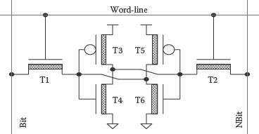
FIGURE 44.1 6T SRAM cell. (Z. Zhang and J.G. Delgado-Frias, Low power and metallic CNT tolerant CNTFET SRAM design, 2011 11th IEEE Conference on Nanotechnology (IEEE-NANO), Portland, OR, August 15–18, 2011, pp. 1177–1182, © (2011) IEEE. With permission.)
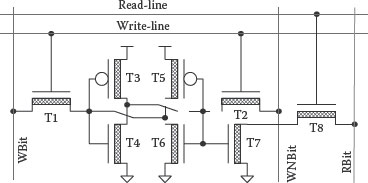
FIGURE 44.2 8T SRAM cell. (Z. Zhang and J.G. Delgado-Frias, Low power and metallic CNT tolerant CNTFET SRAM design, 2011 11th IEEE Conference on Nanotechnology (IEEE-NANO), Portland, OR, August 15–18, 2011, pp. 1177–1182, © (2011) IEEE. With permission.)
44.2.2 EIGHT-TRANSISTOR SRAM CELL
An eight-transistor (8T) memory cell is shown in Figure 44.2. This 8T SRAM cell has a similar structure as 6T with two additional transistors that decouple the read and write operations. The read operation is performed by setting the read-word line to logic 1; the additional transistors (T7 and T8) discharge the RBit line that has been precharged before the Read-line is set. The 8T basic cell provides a more orthogonal design; the read and write operations are performed by different transistors. Since the read operation does not affect the contents of the cell (the two back-to-back inverters), the worst-case SNM is simply that for two cross-coupled inverters [10]. For a 6T cell, on the other hand, the worst-case SNM occurs in the read condition.
44.3 PERFORMANCE OF CNTFET SRAM CELLS
Simulations have been performed using HSPICE and CNTFETs parameter models by Stanford University’s Nanoelectronics Group [11, 12 and 13]. The simulations assume memory arrays with 256 cells to evaluate performance with significant capacitive loading on the bit lines. The nominal chirality of the CNTs is (19, 0) and the pitch is 20 nm. The number of CNTs per transistor for the 6T SRAM cell is T1 (3), T2 (3), T3 (3), T4 (3), T5 (1), and T6 (1). For the 8T cell, the number of CNTs per transistor is T1 (6), T2 (6), T3 (1), T4 (1), T5 (1), T6 (1), T7 (12), and T8 (12). Table 44.1 shows the performance of the two SRAM cells in terms of access delays, energy, and power. From Table 44.1, it can be observed that the 8T cell has a lower write delay than the 6T cell. This is attributed to having two ports (WBit and WNBit buses) that write simultaneously to the cell and smaller inverter transistors. The 8T cell read delay is significantly smaller than the 6T read delay (69.4%). Since the 6T cell has to discharge either the Bit or NBit bus, this makes it difficult to increase the current driving capability of the n-type transistors without greatly affecting the write delay. The energy and dynamic power for the 8T cell are slightly higher; these metrics are measured when the R-line needs to be precharged. If a 1 was read previously, this line is already at a high; this is not the case with 6T, which needs to precharge a line at every read. When a read occurs, the precharged bit lines affect either the stored bit or its inverse (the cross-coupled inverter inputs). Although this voltage change is not enough to change the state of the memory cell, the circuit consumes power to retain the proper voltage.
TABLE 44.1
Performance of SRAM Cells on Read and Write Delay, Energy, and Static Power
|
SRAM Cell |
||
Parameters |
6T |
8T |
Comparisona |
Write delay (ps) |
3.06 |
2.46 |
−19.5% |
Read delay (ps) |
29.23 |
8.96 |
−69.4% |
Max delay (ps) |
29.23 |
8.96 |
−69.4% |
Energy (fJ) |
1.62 |
1.83 |
13.2% |
Static power (nW) |
0.185 |
0.110 |
−40.5% |
Source: Z. Zhang and J.G. Delgado-Frias, Low power and metallic CNT tolerant CNTFET SRAM design, 2011 11th IEEE Conference on Nanotechnology (IEEE-NANO), Portland, OR, August 15–18, 2011, pp. 1177–1182, © (2011), IEEE. With permission
a Percentage comparison calculation: 100(8T value–6T value)/6T value.
In a large memory array, static power becomes a dominant factor in power consumption. Static power has a multiplicative effect; all cells in the array are drawing this power. The 8T cell reduces this static power by 40% in simulations with nominal parameter values.
44.4 PERFORMANCE OF CNTFET SRAM CELLS UNDER PARAMETER VARIATIONS
Paul et al. [8] report that the process parameter that, when varying, affects CNTFETs the most is the diameter. When varied, the effective channel length, oxide thickness, dopant fluctuation, and so on show weak influence on the gate capacitance and drive current of CNTFETs. The device width is another parameter that influences the gate capacitance and drive current. The width of a CNTFET is given by the number of tubes per transistor. This number has been adjusted to achieve the proper operation of each memory cell. The device widths, that is, the number of CNTs per transistor, are not varied any further.
The impact of the power supply voltage, pitch, and temperature variations on 6T and 8T SRAM cells’ delay, energy, and leakage power is reported in Refs. [14,15]. That study showed that a supply voltage reduction of 44.4% (from 0.9 to 0.5 V) decreased energy by 71.2% and 69.5% and increased delay by 65.4% and 168.6% for the 6T and 8T cells, respectively [14]. Temperature has no major impact on delay and energy. However, temperature has a great effect on leakage power by an order of magnitude. The static power goes from 1.1 and 0.76 nW (at 27°C) to 11.5 and 8.06 nW (at 100°C) for 6T and 8T SRAM cells, respectively.
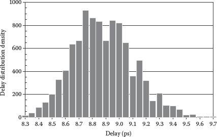
FIGURE 44.3 8T write delay distribution density with random diameter variation. (Z. Zhang and J.G. Delgado-Frias, Low power and metallic CNT tolerant CNTFET SRAM design, 2011 11th IEEE Conference on Nanotechnology (IEEE-NANO), Portland, OR, August 15–18, 2011, pp. 1177–1182, © (2011) IEEE. With permission.)
CNT diameter variations have a large impact on the current that a CNTFET can drive [8], affecting the SRAM cell’s read and write delays. If the diameter of all the CNTFETs is set to be 10% smaller or 10% larger than the nominal diameter, the read delay is increased by 32.1% or decreased by 13.8%, respectively [15]. A smaller diameter than the nominal CNT diameter has a larger impact on delay. Figure 44.3 shows the write delay of RAM cells with randomly distributed diameters of ±10% of nominal; each memory cell has CNTs that have different diameters. This, in turn, is a more realistic simulation of diameter variations in a memory cell. Since smaller diameters have a larger effect on delay, the distribution is asymmetric with a larger tail toward longer delays. Thus, it is necessary to pay particular attention to the configuration of the circuit/transistor that might be most impacted by diameter variations.
Figure 44.4 shows how the static power of the cell is affected by diameter variations. A 16 × 16 SRAM array with nominal diameter leaks current of 0.763 nW with a 0.9 V power supply. The ±10% variation could cause static power change from −55.8% to 95.8%.
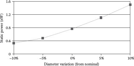
FIGURE 44.4 Diameter variation impact on static power. (Z. Zhang and J.G. Delgado-Frias, Low power and metallic CNT tolerant CNTFET SRAM design, 2011 11th IEEE Conference on Nanotechnology (IEEE-NANO), Portland, OR, August 15–18, 2011, pp. 1177–1182, © (2011) IEEE. With permission.)
44.5 CNTFET SRAM CELL WITH METALLIC CNTS
Current CNT synthesis techniques grow metallic CNTs along with semiconductor CNTs. Metallic CNTs essentially form resistive shorts between the source and drain of a CNTFET. It is expected that new techniques will be developed to reduce the number of metallic CNTs to less than 5%. For instance, Zhang et al. developed a novel process of selective etching that removes a large number of metallic CNTs [16]. In this study, we use a technique to tolerate these metallic CNTs that yield CNTFETs.
An array of series and parallel individual CNTFETs is used to tolerate metallic CNTs to obtain a semiconductor CNTFET. Figure 44.5 shows how a CNTFET transistor can be built using this array [17]. Each CNTFET has two CNTs. The 3 × 2 array of transistors has three transistors in series with uncorrelated (independent) CNTs; this array also has two transistors in parallel with correlated (identical) CNTs. The parallel transistors share common nodes, resulting in a compact layout.
Based on this structure, the probability of having a CNTFET is calculated [17]. Before getting the probability, some terms/definitions are presented (the value for the example in Figure 44.5 is given within parentheses).
Psemi = probability that the CNT is a semiconductor
n = number of CNTs per CNTFET (n = 2)
j = number of series CNTFETs (j = 3)
k = number of parallel CNTFETs (k = 2)
The probability of having an n-type CNTFET (where all the tubes are semiconductor CNTs) is
(44.1) |
Having j CNTFETs in series with uncorrelated (independent) CNTs yields the series probability (a CNT can be either a semiconductor or metallic CNT; a semiconductor series is produced when at least one semiconductor CNT is present in each CNTFET).
(44.2) |
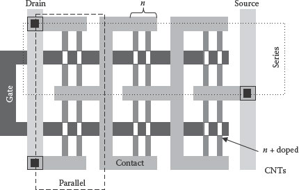
FIGURE 44.5 A transistor with series–parallel CNTFETs. (Z. Zhang and J.G. Delgado-Frias, Low power and metallic CNT tolerant CNTFET SRAM design, 2011 11th IEEE Conference on Nanotechnology (IEEE-NANO), Portland, OR, August 15–18, 2011, pp. 1177–1182, © (2011) IEEE. With permission.)
Transistors in series greatly increase the probability of having a semiconductor CNTFET. Series CNTs, however, decrease the ON current (ION). Parallel CNTFETs that use correlated (identical) CNTs help to increase ION. Having parallel transistors with correlated CNTs does not affect the overall probability. Thus, the probability of having a transistor including the Psemi term is
(44.3) |
Using series and parallel CNTFETs, we propose an approach where the same CNTs are used to form different transistors. In the memory cell, the CNTs run in the vertical orientation. CNTs in the same vertical line are identical; portions of some CNTs are etched to form different transistors. Using the proposed approach results in identical transistor pairs: T1–T2 (write), T3–T5 (inv_p), T4–T6 (inv_n), and T7–T8 (read). Transistors T1, T2, T7, and T8 have both series and parallel individual transistors. Thus, the memory cell’s probability is
(44.4) |
where Pwrite is the probability of having T1 (or T2 since they are identical) as a semiconductor transistor; thus, Equation 44.3 can be used. In a similar fashion, Pinv_p, Pinv_n, and Pread are the probabilities of having T3 (or T5), T4 (or T6), and T7 (or T8) as semiconductor transistors, respectively. The number of series transistors is the same for all the transistors. The number of CNTs per CNTFET is set to 1 (n = 1). It should be mentioned that, depending on the required ON current (ION), the number of parallel transistors could vary in each transistor of the memory cell. Using Ptransistor expression from Equation 44.3, the memory cell probability becomes (with n = 1)
(44.5) |
The proposed scheme reduced the number of terms in the PMem_cell expression from eight individual probabilities to just four. Table 44.2 shows the probability of having a functional 6T and 8T SRAM cells, given a Psemi of 0.9 and 0.95. In this table, the number of CNTFETs in series (j) is increased from 1 to 6.
The memory cell probability depends on one transistor per pair. Parallel transistors provide additional paths to increase ION. For the 8T SRAM cell, the back-to-back inverters (T3, T4, T5, and T6) only hold the stored bit; thus, the inverter transistors need not have parallel transistors. Table 44.3 shows the number of parallel transistors (k) along with the series transistors (j). The 8T cell has two sets of values for k for each value of j. The first set is optimized to obtain a short delay. The second set (labeled as 8Tk.min) is set to have the minimum number of parallel transistors; this, in turn, leads to smaller SRAM cells.
TABLE 44.2
6T and 8T Memory Cell Probability Pmem_cell (with n = 1)
|
Psemi = 0.9 |
Psemi = 0.95 |
||
j |
6T |
8T |
6T |
8T |
1 |
0.729 |
0.6561 |
0.857375 |
0.814506 |
2 |
0.970299 |
0.960596 |
0.992519 |
0.990037 |
3 |
0.997003 |
0.996006 |
0.999625 |
0.9995 |
4 |
0.9997 |
0.9996 |
0.999981 |
0.999975 |
5 |
0.99997 |
0.99996 |
0.999999 |
0.999999 |
6 |
0.999997 |
0.999996 |
1 |
1 |
Source: Z. Zhang and J.G. Delgado-Frias, Low power and metallic CNT tolerant CNTFET SRAM design, 2011 11th IEEE Conference on Nanotechnology (IEEE-NANO), Portland, OR, August 15–18, 2011, pp. 1177–1182, © (2011) IEEE. With permission
TABLE 44.3
j (Series) and k (Parallel) CNTFETs for SRAM Cells
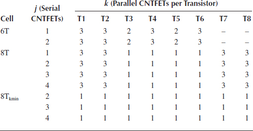
The 6T cell structure is chosen to have appropriate read and write operations according to Ref. [18]. The 8T cell is designed to have the same number (16) of CNTs with the 6T cell in the j = 1 case. The read performance for 6T and 8T will be close since they both have three CNTs to discharge the bit lines while reading; the 8T cell will have a shorter write delay because its inverter pair has the minimum size.
We are considering two cases in the optimization of the 8T SRAM cell: having parallel transistors (larger k) to obtain short read delays, and having the minimum number of parallel transistors (kmin) to minimize the required CNTs per SRAM cell. With the j and k parameters specified in Table 44.3, simulations of the 6T and 8T SRAM cells were performed. Table 44.4 shows the delay, energy, static power, and SNM of the different 6T, 8T, and 8T with kmin memory cell configurations. Figures 44.6 and 44.7 show the information in a graphical manner. As j is increased, both the write and read delays increase. The required energy to write (0 or 1) increases much faster for the 6T cell as j increases; this is due to the need to have strong n-type transistors for the read operation. The 8T cells do not require energy to read a “1”; if reading a “1” becomes dominant, more energy is saved. It should be pointed out that the static power drops drastically as j increases. This is due to having transistor in series or the stack effect [19], which also applies to the CNT-based circuits.
It should be pointed out that the 8T cell requires no parallel transistors for the inverters since they are only needed to hold the stored bit but not to drive a large load. Thus, the static power due to drain source leakage remains low for the 8T cell. From Table 44.4, it can be observed that static power of the 6T cell for j = 2 is 1.74 times higher than the 8T cell with the same j, and the SNM of the 6T cell is approximately 100 mV below all the 8T cells.
Having a minimum value of k (i.e., minimum number of parallel CNTFETs per transistor) has an impact on the write delay and a much greater impact on the read delay. This is shown in Figure 44.8. Write to a cell is done by external drivers while read operations are driven by the cells that need to discharge the bit line.
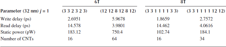
To reduce delays in a particular read delay, it is necessary to increase the number of CNTs (k variable) in the cells. Table 44.5 shows both the 6T and 8T cell structures with k specified in parentheses for each cell. To reduce the delay, larger k values are required to increase the driving current. The 6T cell structure limits the flexibility for the design trade-off between speed and stability. By maintaining the same SNM, we increase the k values to (12 12 8 12 8 12) for (T1 T2 T3 T4 T5 T6). As is shown in the second column for 6T in Table 44.5, the read delay is reduced to 3.98 ps; the write delay, on the other hand, is increased to 5.9678 ps, which is even longer than the read delay. This is due to the larger capacitive loads on the internal inverter pair, which means higher energy is required to change the stored value. The static power increases by four times due to the number of parallel CNTs in the internal inverters. On the other hand, reducing the read delay on the 8T cell due to its orthogonal design requires an increase in the size of transistors T7 and T8. Thus, with k = (3 3 1 1 1 1 12 12), a similar read delay to the improved 6T cell can be achieved. The 8T write delay is slightly increased (2.7572 ps) due to the larger read transistor pair. The new 8T cell has a similar static power as the original 6T cell. The decoupled read and write characteristic of this cell structure ensures that its inverters can stay with the minimum size while improving the dynamic read performance. It should be noted that the improved 8T cell outperforms the improved 6T cell with about half the total CNT counts.
TABLE 44.4
6T, 8T, and 8Tkmin Performance
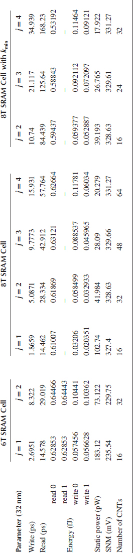
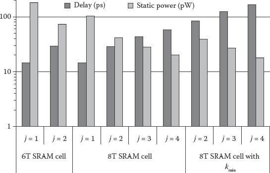
FIGURE 44.6 Delay and static power comparison of various cell structures for the 32 nm technology node.
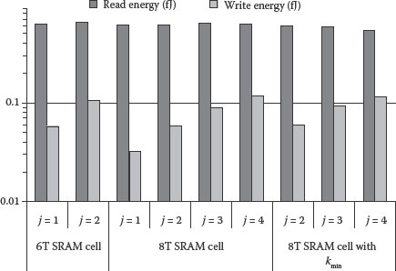
FIGURE 44.7 Read and write energy comparison of various cell structures for the 32 nm technology node.
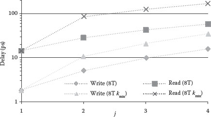
FIGURE 44.8 Read and write delays of 8T and 8T with kmin SRAM cells.
TABLE 44.5
Performance of the SRAM Cell with Different Cell Sizes (j = 1, Larger k)
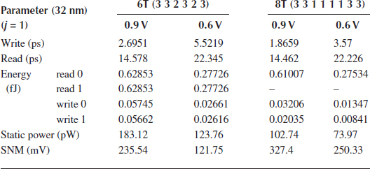
Reducing the power supply would slow down the circuit but has the potential of saving energy. Table 44.6 presents the data for the 6T and 8T cells in this chapter with different two power supplies (0.9 and 0.6 V). It can be observed that for both cells the worst-case delay is increased from 14.5 to 22.3 ps (53.7%), but the energy during the read or write activities are reduced by around 55.9%. As expected, the SNM degrades with lower power supply voltage. However, the 8T cell with VDD = 0.6 V still outperforms the 6T cell with 0.9 V in terms of SNM.
TABLE 44.6
Low-Power Performance for SRAM Cell in 32 nm Technology
44.6 OPTIMIZATION OF THE PERFORMANCE OF THE CELL AND FUNCTIONAL PROBABILITY
In this section, we present an approach to optimize the 8T SRAM cell design; we use j = 3 as an example. Several sets of the k values are simulated using HSPICE; we use k1, k2, k3, and k4 as the number of parallel CNTFETs in the write transistor pair T1–T2, inv_n pair T4–T6, inv_p pair T3–T5, and read pair T7–T8, respectively. In the following figures and tables, the combinations are denoted in parentheses as (k1, k2, k3, k4). A (19, 0) semiconducting CNT chirality has been selected as the standard. The 8T SRAM cell has a read–write orthogonal design, and the read delay of the cell is determined by k4 (transistors T7 and T8) with virtually no influence of the other transistor sizes. The larger number of CNTs in k4 reduces this delay at the expense of larger cells.
To evaluate the performance of the SRAM cell with metallic CNT tolerance, 20,000 simulations based on Monte Carlo randomization have been performed on three different cell sizes; cell size is determined by both j and k parameters; in this particular example, j is constant. The cell sizes are the minimum-k (1,1,1,1), (2,1,1,4), and (3,1,1,8). Table 44.7 shows the average write delay of the different combinations. It can be observed that write delay is influenced by k1. As k1 is made larger (or stronger), the write delay decreases. Having metallic CNTs may render some SRAM cells as nonfunctional; these cells may have short circuits. When all the CNTs that form a transistor are metallic, we refer to this problem as a short transistor; these are reported in the third column of the table. Another problem is called write failure; this is due to a combination of having stronger inverters and weaker write transistors. With j = 3, a transistor that has one or two metallic CNTs is able to deliver higher current and thus is stronger than the CNTFET, which has no metallic CNTs. As k1 is made larger than 1, the write failure problem is greatly reduced as shown in Table 44.7. Since the read delay is the dominant delay for this cell, the write delay is not a factor in the cell functionality.
The write and read delay distributions for the last two cell structures (2,1,1,4) and (3,1,1,8) in our study are shown in Figures 44.9 and 44.10, respectively. Most of the delays are centered at their standard delay values with a long tail in each case. The read delay could be reduced by increasing the transistor array size. However, this comes at the expense of additional hardware (i.e., more CNTs). Figure 44.11 illustrates the distribution of SNM of the two cells. In both cases, the SNM values are above 280 mV and centered at 330 mV. The high correlation between the two curves suggests that the size of either write or read transistor pairs has very little influence on the SNM.
TABLE 44.7
Cell Structure, Write Delay, Cell Failure: Short Transistor and Write Fail
Cell Structurea |
Write Delay (ps) |
Short Transistor (%) |
Write Fail (%) |
Total Nonfunctional (%) |
(1,1,1,1) |
21.117 |
0.45 |
2.59 |
96.96 |
(2,1,1,4) |
14.886 |
0.41 |
0 |
99.59 |
(3,1,1,8) |
13.555 |
0.43 |
0 |
99.57 |
a Number of CNTs in transistor pair (k1, k2, k3, k4).
Transistors included in transistor pair: k1 [T1,T2], k2 [T4,T6], k3 [T3,T5], k4 [T7,T8].
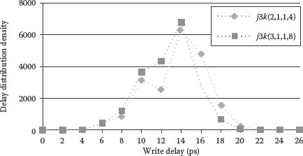
FIGURE 44.9 Write delay distribution density.
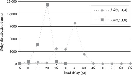
FIGURE 44.10 Read delay distribution density.
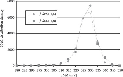
FIGURE 44.11 SNM distribution density.
44.7 MEMORY WITH SPARE COLUMNS
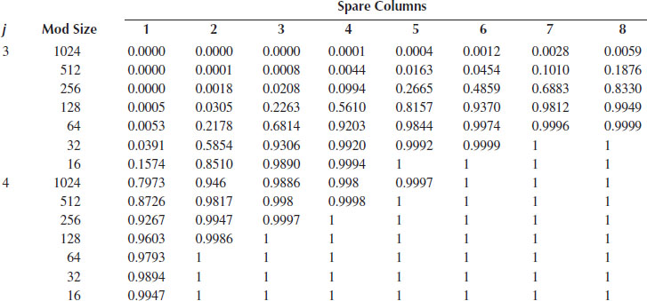
Building a large memory out of SRAM cells in the presence of metallic CNTs requires a fault-tolerant scheme to overcome faulty memory cells. For this study, we have chosen spare columns to deal with faults. This scheme was chosen because it is simple and achieves the goal of having functional memory. Table 44.8 shows the probability of having a functional 1024 × 32 bit memory. The parameter setting is as follows: Psemi is 95%, the number of transistors in series (j) is 3 and 4, and k is specified in Table 44.3. The large memory is divided into smaller modules that go from a single module of 1024 entries to a module of 16 entries. From this table, it can be seen that a small value of j (i.e., 3) would require a large number of spare columns to yield a functional memory.
TABLE 44.8
Probability of Functional Memory with Spare Columns
Source: Z. Zhang and J.G. Delgado-Frias, Low power and metallic CNT tolerant CNTFET SRAM design, 2011 11th IEEE Conference on Nanotechnology (IEEE-NANO), Portland, OR, August 15–18, 2011, pp. 1177–1182, © (2011) IEEE. With permission.
As the modules have fewer entries, the number of columns needed decreases. It can be observed that 64- or 32-entry modules (for j = 4) yield a good probability of a functional memory. Figure 44.12 shows the same information in a graphical manner.
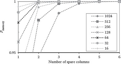
FIGURE 44.12 P as a function of the number of spare columns and module size for j = 4.
So far, we have discussed the performances and evaluated the functionality of a CNT-based SRAM cell at the 32 nm technology node. In this section, we show the performance of the CNTFET memory cells at 22 and 16 nm technologies. The process parameters for 22 and 16 nm N-type CNTFET are listed in Table 44.9. The 32 nm CNTFET parameters are from the values included in the Stanford University CNTFET HSPICE Model [11], and the 16 nm CNTFET values are compiled from a study by Yanan Sun et al. [20]. The supply voltage drops from 0.9 to 0.7 V as the technology is scaled down, and dielectric materials with high k values are used to maintain the same driving current and reduce leakage current.
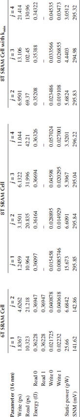
Tables 44.10 and 44.11 present the performances of the 6T and 8T cells under 22 and 16 nm technology. It can be observed that all the delays and power dissipations decrease as the transistor size is scaled down. The 22 nm 6T and 8T cells take only 85% of the time, and the 32 nm cells need to read 0, while dissipating about 76% energy because of the reduced capacitive loads and lower power supply. The improvement for 16 nm cells is 75% in read delay and 60% in read energy. The static power for 22 nm cells is only about 40~60% of the amount for 32 nm. The 16 nm cells dissipate only 9–19% of the static power compared to the 32 nm counterparts. The only parameter that is degraded is the SNM. For the 8T cells, the lower power supply can still hold the SNM at about 97% for 22 nm and 90% for 16 nm of the 32 nm SNM. The 6T cells are more vulnerable to noise; their values drop around 20% and 40% for 22 and 16 nm technologies, respectively.
In this chapter, we have presented the design of a CNTFET-based memory system that has a simple metallic CNT tolerance. Some features of the 8T CNTFET SRAM and memory modules include:
• CNTFET SRAM cell tolerant to metallic CNT. Metallic CNT tolerance is accomplished by having a series of CNTs to form a transistor. With j = 3, the probability of a nonfunctional cell can be as low as 99.59%; the worst-case delay and SNM are as high as 30 ps and 350 mV, respectively.
TABLE 44.9
Process Parameters for 32, 22, and 16 nm CNTFET
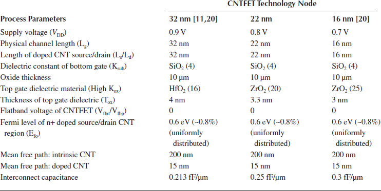
TABLE 44.10
6T, 8T, and 8Tkmin Performance at 22 nm
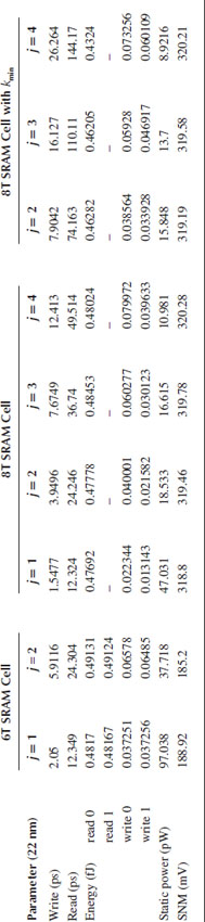
TABLE 44.11
6T, 8T, and 8Tk min Performance at 16 nm
• Low static power. Leakage current is one of the major contributors in the power consumption in SRAM arrays. The 32 nm 8T CNTFET SRAM cell’s static power stays between 20.79 and 102.74 pW with different j and k configurations. The 6T static power with j = 2 is 1.47 times higher than the 8T cell with j = 2. The leakage current drops drastically as j increases.
• High SNM. The 8T cell’s SNM is higher than the 6T’s SNM. For all the configuration of the 8T, the SNM range is between 327 and 331 mV while the 6T’s range is between 229 and 235 mV. With the power supply lowered from 0.9 to 0.6 V, the 8T cell’s SNM drops by 23.5%, while the 6T cell’s SNM drops by 48.3%.
• Small cell size. The delay can be improved by having more parallel CNTs; the 8T cell achieves similar read and write delays using about half the number of CNTs in the 6T cell.
• Low k (parallel FETs) values. The 8T cells can tolerate low values of k; this, in turn, impacts the read delay.
• Spare columns to tolerate faulty SRAM cells. By means of a simple fault-tolerant scheme, the proposed SRAM cell can be used to form a large memory system.
• Orthogonal design space for read and write. Decoupled write and read operations provide an orthogonal design space that helps to balance speed and area. 6T cells, on the other hand, require a great deal of design effort to ensure proper read and write operations.
• Read delay of the 8T cell without metallic nanotubes tends to cluster around 8.9 ps with random ±10% diameter variations. A Monte Carlo simulation shows a delay distribution with a mean of 8.91 ps. Owing to the nonlinear effect of diameter variation on current, the delay distribution extends to the longer delays.
• Low energy (dynamic power) for writing. While performing a write into an 8T cell, smaller gate capacitance is engaged in restoring the cell’s value due to the minimum-sized inverter pair.
• Robustness to technology scaling. SRMA cells at 22 and 16 nm technologies reduce the delay by 15% and 25%, respectively. Both dynamic and static power consumptions are also reduced by up to 24% and 60% for 22 nm, and 43% and 91% for 16 nm. 8T cells maintain a higher SNM than 6T cells as technology scales down.
As new techniques to grow CNTs reduce the number of metallic CNTs, the proposed memory system will require lower j (fewer CNTFETs in series) and fewer spare columns.
The research reported in this chapter has been partially supported by WSU’s Boeing Centennial Endowed Chair.
1. T.-C. Chen, Overcoming research challenges for CMOS scaling: Industry directions, International Conference on Solid-State and IC Technology, Shanghai, China, pp. 4–7, October 23–26, 2006.
2. T. Cakici, K. Kim, and K. Roy, FinFET based SRAM design for low standby power applications, 8th International Symposium on Quality Electronic Design, San Jose, CA, pp. 127–132, March 26–28, 2007.
3. Y. B. Kim, Y.-B. Kim, and F. Lombardi, New SRAM cell design for low power and high reliability using 32 nm independent gate FinFET technology, IEEE International Workshop on Design and Test of Nano Devices, Circuits and Systems, Cambridge, MA, pp. 25–28, 2008.
4. International Technology Roadmap for Semiconductors, http://www.itrs.net/.
5. A. Lundstrom, A top-down look at bottom-up electronics, 2003 Symposium on VLSI Circuits, Digest of Technical Papers, Kyoto, Japan, pp. 5–8, June 12–14, 2003.
6. P. H.-S. Wong, Field effect transistors-from silicon MOSFETs to carbon nanotube FETs, 23rd International Conference on Microelectronics, Nis, Yugoslavia, pp. 103–107, May 12–15, 2002.
7. P. Avouris, Z. Appenzeller, R. Martel, and S. Wind, Carbon nanotube electronics, Proceedings of the IEEE, 91(11), 1772–1784, November 2003.
8. B. C. Paul, S. Fujita, M. Okajima, T. H. Lee, P. H.-S., Wong, and Y. Nishi, Impact of a process variation on nanowire and nanotube device performance, IEEE Transactions on Electron Devices, 54(9), 2369–2376, September 2007.
9. Y. B. Kim, Y.-B. Kim, F. Lombardi, and Y. J. Lee, A low power 8T SRAM cell design technique for CNTFET, IEEE International SoC Design Conference (ISOCC), Pusan, South Korea, pp. 176–179, November 24–25, 2008.
10. L. Chang, R. K. Montoye, Y. Nakamura, K. A. Batson, R. J. Eickemeyer, R. H. Dennard, W. Haensch, and D. Jamsek, An 8T-SRAM for variability tolerance and low-voltage operation in high-performance caches, IEEE Journal of Solid-State Circuits, 43(4), 956–963, April 2008.
11. CNTFET Models. http://nano.stanford.edu/models.php.
12. J. Deng and H.-S. P. Wong, A compact SPICE model for carbon nanotube field effect transistors including non-idealities and its application—Part II: Full device model and circuits performance benchmarking, IEEE Transactions on Electron Devices, 54(12), 3195–3205, December 2007.
13. J. Deng and H.-S. P. Wong, A compact SPICE model for carbon nanotube field effect transistors including non-idealities and its application—Part I: Model of intrinsic channel region, IEEE Transactions on Electron Devices, 54(12), 3186–3194, December 2007.
14. J. G. Delgado-Frias, Z. Zhang, and M. A. Turi, Low power SRAM cell design for FinFET and CNTFET technologies, International Conference on Green Computing, Chicago, IL, pp. 547–553, 2010.
15. Z. Zhang, Y. Liu, J. Nyathi, and J. G. Delgado-Frias, Performance of CNFET SRAM cells under diameter variation corners, MWSCAS 2009. 52nd Midwest Symposium on Circuits and Systems, Cancun, Mexico, pp. 547–550, August 2–5, 2009.
16. G. Zhang, P. Qi, X. Wang, Y. Lu, X. Li, R. Tu, S. Bangsaruntip, D. Mann, L. Zhang, and H. Dai, Selective etching of metallic carbon nanotubes by gas-phase reaction, Science, 314, 974–977, 2006.
17. A. Lin, N. Patil, H. Wei, S. Mitra, and H.-S. P. Wong, A metallic-CNT-tolerant carbon nanotube technology using asymmetrically-correlated CNTs (ACCNT), 2009 Symposium on VLSI Technology, Honolulu, HI, pp. 182–183, 2009.
18. S. Lin, Y.-B. Kim, F. Lombardi, and Y. J. Lee, A new SRAM cell design using CNTFETs, SoC Design Conference, 2008. ISOCC ‘08. International, 01, Busan, South Korea, pp. I-168–I-171, November 24–25, 2008.
19. C. Zhanping, M. Johnson, W. Liqiong, and W. Roy, Estimation of standby leakage power in CMOS circuit considering accurate modeling of transistor stacks, Proceedings of the 1998 International Symposium on Low Power Electronics and Design, 1998, Monterey, CA. pp. 239–244, August 10–12, 1998.
20. Y. Sun and V. Kursun, N-type carbon-nanotube MOSFET device profile optimization for very large scale integration, Transactions on Electrical and Electronic Materials, 12(2), 43–50, April 25, 2011.
21. Z. Zhang and J. G. Delgado-Frias, Low power and metallic CNT tolerant CNTFET SRAM design, 2011 11th IEEE Conference on Nanotechnology (IEEE-NANO), Portland, OR, pp. 1177–1182, August 15–18, 2011.