
Optimized Built-In Self-Test Technique for CAEN-Based Nanofabric Systems |
CONTENTS
45.1.1 Benefits and Challenges of Nanotechnology
45.2 Background and Related Works
45.2.1 Novel Logic Mapping Technique
45.3.2 Test Architectures and Procedure
45.3.4 Algorithm for Locating Defects and Example Defect Detection
45.3.5 Example of a Faulty Block Identification
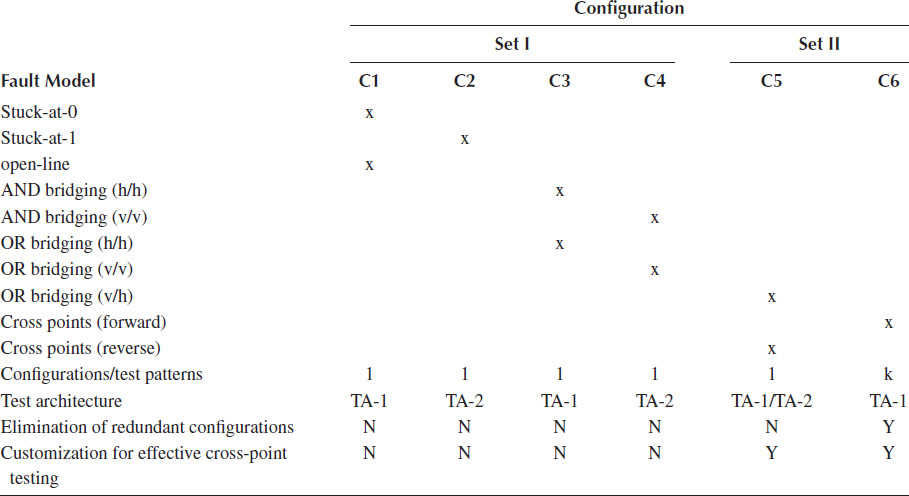
45.3.6 Design of New BUT Configurations and Test Patterns and Fault Coverage Analysis
45.3.7 Configuration C1: Stuck-at-0 and Stuck-Open Faults
45.3.8 Configuration C2: Stuck-at-1 Faults
45.3.9 Configuration C3: AND/OR Bridging Faults (h/h)
45.3.10 Configuration C4: AND/OR Bridging Faults (v/v)
45.3.11 Configuration C5: Reverse-Biased Diode and v/h Bridging Faults
45.3.12 Configuration C6: Forward-Biased Diode Faults
45.3.13 Fault Coverage and Number of Configurations
45.4.1 Elimination of Redundant Configurations
45.4.2 Customized Configurations
45.5.1 Number of Configurations/Test Patterns
Nanotechnology enables future advancements in integrated circuitry’s miniaturization, energy and cost efficiency, and capabilities. However, a popular, chemically assembled electronic nanotechnology (CAEN) has a high rate of defects that negates these benefits of the nanofabric. To address this challenge, we propose a testing technique that maximizes the yield from a nanofabric while minimizing the testing overhead. In contrast, traditional testing techniques, for example, the ones employed in field programable gate array (FPGA) applications, assume a low defect rate and fail to achieve high effectiveness when applied to testing nanofabrics. In this chapter, we propose a novel approach to testing a nanofabric that includes new testing configurations, test-set optimization methodology, and design of customized configuration, which provide a reduction in testing time while enhancing the utilization of the nanofabric. Part of the proposed scheme is a recovery procedure that further increases the utilization of nanoblocks at the expense of testing time. The proposed procedure tests all the components in parallel and identifies the defective nanoblocks in a nanofabric. A defect map is generated to aid logic function implementation in a nanofabric. The proposed technique results in less number of test configurations compared to other proposed methods and a significant reduction in the test time.
45.1.1 BENEFITS AND CHALLENGES OF NANOTECHNOLOGY
Moore’s law predicted that the number of transistors that could be placed on a chip doubles every 2 years. The complementary metal oxide semiconductor (CMOS) technology has been able to keep up with Moore’s law as a result of scaling. However, CMOS technology today faces a number of challenges such as leakage currents, process variation, costs, and reliability issues, which may put an end to scaling. Therefore, new technologies are needed to replace CMOS in the future to continue Moore’s law advancement.
CAEN has shown promising potential for the future of nanoscale design [1, 2 and 3]. A basic building block of a nanofabric is a nanoblock, which is an interconnected 2D array of nanoscale wires that can be electronically configured as logic networks, memory units, and signal-routing cells [4,5]. These nanofabric architectures are reconfigurable in nature and can achieve a density of 1010–1012 gates per cm2, which is significantly higher than that of CMOS-based devices. However, owing to the high defect rate in these nanofabrics, new testing strategies need to be devised to effectively test and diagnose the nanofabric within a reasonable time.
The low-cost manufacturing process of self-assembly and self-alignment is associated with a high defect rate approaching 10%, thus lowering the yield and increasing the manufacturing costs. It is impractical to throw away a fabricated chip once it is diagnosed to be defective. Thus, a defect-tolerant approach is required such that partially defective blocks can be utilized. The ability to identify and diagnose the faulty sites on a chip and develop techniques to avoid these faulty areas is known as defect tolerance [4,6, 7, 8, 9, 10 and 11]. Also, the testing techniques needed for nanofabrics are complicated due to the large density, high defect rate, and large size of the nanoblocks. Hence, traditional FPGA testing approaches [12,13] are not suitable for the nanofabric systems.
In this chapter, we discuss a testing methodology for nanofabric systems that configures the components as block under tests (BUT) and comparators (C). This method allows us to handle high defect densities and large-size nanofabrics. Our method uses a set of test architectures and BUT configurations to test the nanofabric. Also, we explain the design of each of the BUT configurations for the targeted faults. An external tester is used to apply test patterns to the BUTs. The nanoblocks are tested in parallel, and hence the testing time does not depend on the size of the nanofabric. Further, we introduce an optimization technique, which can increase both the testing speed and the usability (yield) of the nanoblock.
45.2 BACKGROUND AND RELATED WORKS
First, the basic concept of the nanofabric-based digital circuits is presented. Then an example application of the self-test procedure is discussed in the context of a reconfigurable digital logic design.
The nanofabric is a regular architecture consisting of a two-dimensional array of interconnected nanoblocks and switchblocks as shown in Figure 45.1. A nanoblock and a switchblock are two main components in a nanofabric. A nanoblock in a nanofabric is similar to a configurable logic block (CLB) in FPGA. A nanoblock is based on a molecular logic array (MLA). There is a reconfigurable switch at each intersection of MLA in series with the diode. Diode-resistor logic is used to perform logical operations. The region between a set of nanoblocks is known as a switchblock that connects wire segments of adjacent nanoblocks. The configuration of the switchblock determines the direction of data flow between the nanoblocks. The detailed explanation of the nanofabric architecture, nanoblocks, and switchblocks can be found in Ref. [14].
The defect tolerance methodology is presented in Ref. [2] such that components of a nanofabric are configured to test circuits to infer the defect status of individual components. Only stuck-at and stuck-open faults are targeted during the test and the proposed technique does not provide high recovery. In contrast, the proposed approach considers additional faults, including nanowire bridging and crosspoint bias. Application-dependent testing of FPGA has also been proposed in Refs. [11,15]. A defective FPGA may pass the test for a specific application. This is a one-time configuration; in other words, the FPGA will no longer be reconfigurable. This reduces yield loss and leads to manufacturing cost savings.
In Ref. [4], testing is performed by configuring the blocks and switches as linear feedback shift registers (LFSR). If the final bit stream generated by LFSR is correct, all the components are assumed to be defect-free. Otherwise, there is at least one faulty component in LFSR. To diagnose, the components in LFSR and other components are used to configure a new LFSR. If the new LFSR is faulty, the component at the intersection of faulty LFSRs is considered defective. A defect database is created after completing the test and diagnosis. In contrast to the proposed methodology, the LFSR-based approach targets only stuck-at and stuck-open faults, thus reducing the recovery rate.
The CAEN built-in self-test (BIST) approach presented in Ref. [9] configures a nanoblock as a tester to test its neighboring nanoblocks. Test patterns are fed to both the tester and the nanoblock under test (BUT) from an external source. A defect-free BUT generates output patterns that are identical to the input patterns. The tester compares the input test patterns and the output patterns from the BUT to see if the BUT is defective. However, CAEN-BIST is performed in a wavelike manner in which a set of nanoblocks in the same diagonal tests another set of nanoblocks until the entire nanofabric has been tested. Therefore, the complexity and testing time depend on the size of the nanofabric under test.
Another BIST approach was proposed in Ref. [16] where the nanoblocks can be configured as test pattern generators (TPGs), block under test (BUTs), or output response analyzers (ORAs). These blocks, along with the corresponding switchblocks, comprise a TG (test group). In a TG, the TPG generates the testing patterns for a BUT and ORAs examine the BUT output response. A total of 4k + 6 configurations are needed to test for the stuck-at, stuck-open, bridging, and defective crosspoints.
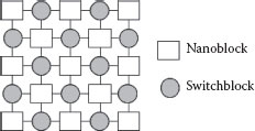
FIGURE 45.1 Nanofabric architecture. (S. Kundaikar and M. Zawodniok, Optimized built-in self-test technique for CAEN-based nanofabric systems, Proceedings of 11th IEEE Conference on Nanotechnology (IEEE-NANO’11), Portland, OR, pp. 1717–1722, © (2011) IEEE. With permission.)
In the BIST procedure discussed in Ref. [17], each nanoblock is configured either as a pattern generator (PG) or as a response generator (RG). A test group is created using a set of PGs, RGs, and switchblock(s) between the two. The nanoblock configured as a PG tests itself and generates the test pattern for RG. An external device is needed to program the nanoblocks and read the RGs’ responses. In the test configurations, stuck-at, stuck-open, forward-biased and reverse-biased diode, and AND and OR bridging faults are targeted. If the size of the nanoblock is k × k, it is estimated that 8k + 5 configurations are needed to provide 100% fault coverage. This number of configurations is still large for a large value of k.
45.2.1 NOVEL LOGIC MAPPING TECHNIQUE
Once the nanofabric is manufactured, it needs to be tested thoroughly to identify the faulty blocks. The testing methodology used will test for certain types and numbers of faults. Once the faulty areas in the chip have been identified, the next step is to map logic onto the nanofabrics by avoiding the faulty blocks. The reconfigurability and functional redundancy within the nanofabric and nanoblocks enable the development of robust, defect-, and fault-tolerant design mechanisms. When a defective resource or component is identified in the chip using test and diagnosis, the postfabrication configuration and logic mapping can counter the effects of those defects. Logic mapping onto nanoblocks refers to the programming of the various cross points of the nanoblock to implement different gates and connecting them together to obtain the required logic function. A nanoblock consists of two groups of parallel nanowires, which are perpendicular to each other in the same plane and programmable cross points at the junction of these nanowires [1]. These cross points can be programmed to behave as diodes by the application of suitable voltage levels. A nanoblock can implement AND/OR gate functionalities by programming the different cross points and by configuring pull-up and/or pull-down resistors. Figure 45.2 illustrates the example implementation of a simple logic by programming the cross points in a nanoblock and the use of pull-up/pull-down resistors. Note that not all cross points are employed in this realization.
The process of logic mapping could be simplified if there were standard configurations of nanoblocks available, which could implement specific functionality. This would reduce the effort needed to design custom configurations for each nanoblock. By configuring a nanoblock, we mean programming the various cross points within the block to implement logic functionality.
We propose a novel logic mapping technique, which would use the result of the testing technique presented in this work. Here, the types of faults targeted are stuck-at faults, bridging, and cross-point faults. It is assumed that each nanoblock implements only AND/OR logic and is tested to make sure it can successfully implement such a configuration. This requires only a certain set of cross points to be fault-free to successfully implement the function. This results in a substantial increase in the yield of the nanofabric. Also, the nanoblocks are assumed to be implementing only AND/OR gates, and the nanoblock configurations are fixed. A k × k nanoblock implementing a (k × 1) input AND/OR gate is shown in Figure 45.3. The F1 output implements the AND function for inputs A1, A2,…, Ak−1, while F2 implements the OR function for the B1, B2,…, Bk−1 inputs. For such a configuration, the effective cross points (required for function realization) are known a priori. Hence, the customized testing, such as the one in Ref. [17], provides a map of useful nanoblocks that can be utilized even if partial defects are present. Consequently, the nanoblocks marked as fault-free can implement AND/OR logic using standard configurations, such as the one in Figure 45.3.
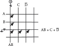
FIGURE 45.2 Simple logic implementation.
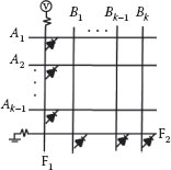
FIGURE 45.3 AND/OR implementation.
The main advantage of such an implementation is that we need not know the location of defects inside the nanoblock. Also, no effort would be needed in designing the nanoblock configurations for each nanoblock since we are using standard AND/OR implementation. This implementation method requires the function to be in the sum of products (SOP) or product of sums (POS) form. Once the function is available in the required form, we need to determine the number of input blocks required to implement the function and also map the functionality to each of the blocks used, that is, whether the block will implement AND logic or OR logic. We need not worry about configuring the blocks internally since we are using standard configurations. Once functionality has been mapped to the nanoblocks, we need to connect them and route the result to the output of the nanofabric. Here, we illustrate this method using three examples.
Consider that we have a simple function Z1 = AB + C + DE. We need a total of two AND and two OR gates to implement this function. Consider that we have a fault-free nanofabric consisting of 36 nanoblocks and that each nanoblock is 3 × 3. The implementation of this function is shown in Figure 45.4. The circles represent switchblocks, which are used to connect the output of one block to the input of the next one. The rectangles represent the nanoblocks that are configured to implement either an AND or OR gate or are just used for routing purposes. As can be seen, the mapping procedure is relatively simpler in the absence of defective blocks. However, in the presence of defects, we need to make sure that we avoid the defective blocks and route the result to the output of the nanofabric.
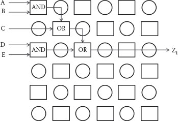
FIGURE 45.4 Logic mapping using AND/OR blocks.
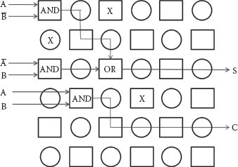
FIGURE 45.5 Half-adder implementation in the presence of defects.
Consider a similar nanofabric with a few defective blocks as shown in Figure 45.5. Here, the defective blocks have been identified by the testing procedure and indicate that they cannot be used to implement any logic. However, in some cases, they may be used to transfer signals from one block to the next. This means that they can be used for routing purposes. Let us implement a half-adder with inputs A, B and outputs sum (S) and carry (C) in the presence of faulty blocks. As can be seen, we need to go around the faulty blocks and find a fault-free path. Thus, in the presence of faulty blocks, we need to use a lot of nanoblocks just for routing around the faulty blocks.
Next, the details of the self-testing approach are presented and discussed.
In this section, a testing approach is presented that efficiently and cost effectively identifies the faulty components. The entire nanofabric is set up based on test architectures to perform a self-test among the nanoblocks. In concert with carefully selected configurations for the nanoblocks under test, the proposed approach minimizes the testing time while ensuring all fault testability. The analysis of the tests results in a defect map that indicates the faulty nanoblocks.
Moreover, we propose two methods that increase the nanofabric yield by identifying partially defective nanoblocks that still can correctly implement the AND/OR logical functions. The proposed optimization approach selects the minimal subset from the entire proposed list of configurations to test for the desired functionality only. Additionally, this test set optimization reduces the overall testing time. The second method, the customization method, redesigns the test configurations such that only the required cross points are tested. In contrast, the optimization technique only reduces the number of unnecessary configurations while still testing the unnecessary cross points. The drawback of the customization method is the need for creating a new set of test configurations for each desired logical function. The increased overhead may result in a longer and more complex testing process.
First, a set of test architectures is presented in Section 45.3.2. Next, the nanoblocks configurations are introduced and discussed in Section 45.3.3. The optimization and customization techniques are proposed in Section 45.4.
45.3.2 TEST ARCHITECTURES AND PROCEDURE
A test architecture (TA) defines the manner in which the nanoblocks and switchblocks are configured and connected. Each of the nanoblocks is configured either as a block under test (BUT) or as a comparator (C) [18] and the switch blocks are used to connect the outputs of BUTs to comparators. A nanoblock configured as a BUT in one TA is configured as a comparator in the other TA. Hence, half of the total number of nanoblocks is tested in each TA. In contrast to the traditional approach utilized in an FPGA-type application, the proposed TAs are constrained by the fabric topology. In a typical nanofabric, nanoblocks have outputs on two sides called the east (right) and the south (bottom). To test the nanoblock functionality in both directions, a total of four TAs are required, as shown in Figure 45.6. The “B” block refers to a nanoblock that is configured as a BUT, and “C” refers to a nanoblock configured as a comparator.
The proposed approach defines two pairs of complementary TAs: TA-1 for outputs on the east side, and TA-2 for outputs on the south side. TA-1b is the complement of TA-1a since a BUT in TA-1a is a comparator in TA-1b and vice versa. Similarly, TA-2b is the complement of TA-2a. The selection of the particular test sets (TA-1a and TA-1b) or (TA-2a and TA-2b) is dictated by the test configuration as discussed in the Section 45.3.3.
The test patterns are applied simultaneously using an external tester. Each comparator compares outputs from two BUTs and each BUT output is connected to two comparators. The output of the comparator will be successful if the BUTs being compared and the comparator itself are defect-free. If any of the BUTs or the comparator itself is faulty, it is an unsuccessful comparison. Since the defect rate is of the order of 10–15%, it is assumed that the probability of two defective BUTs being compared by the same comparator is very low. It is assumed that the comparator generates a “0” for a successful comparison and a “1” for an unsuccessful comparison. This helps generate an intermediate defect map called the partial defect map and, in turn, the final defect map. A test is run for each type of fault to be targeted to create partial defect maps for corresponding faults. Combining all the partial defect maps gives the final defect map, which the compiler can use to configure the nanofabric by avoiding defective blocks.
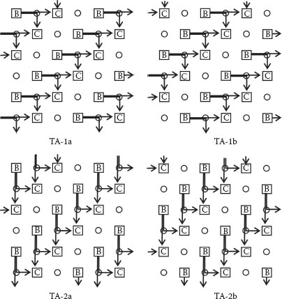
FIGURE 45.6 Test architectures.
A block is declared fault-free only if it does not manifest any of the faults targeted. Initially the final defect map is set to NULL. Next, the BUT configuration is optimized/customized for the targeted fault. A raw defect map is a defect map for a particular fault. For each targeted fault, the raw defect map is initially set to null. The first test architecture is then selected and the corresponding BUT configuration and test patterns are applied. The comparator outputs are read out and the possible faulty blocks are marked as suspects. The complementary test architecture is then applied and the procedure is repeated. The comparator outputs are read out and a decision is made whether the marked blocks are actually faulty or not. Figure 45.7 gives the flowchart for this testing procedure.
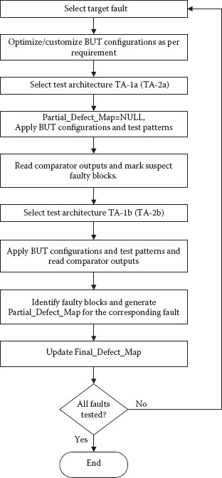
FIGURE 45.7 Testing procedure.
45.3.4 ALGORITHM FOR LOCATING DEFECTS AND EXAMPLE DEFECT DETECTION
The comparator detects inconsistencies between the outputs of two BUTs, which indicate the presence of a fault. To uniquely identify the defective nanoblocks, we need to analyze both (1) outputs of adjacent comparators and (2) test results in the complementary architecture. Once the defect is located, the raw defect map is updated accordingly. The faulty block identification algorithm is presented in Table 45.1. In general, the faulty block is identified when it is marked as faulty by two corresponding comparators. The complementary test architecture is used to identify faults in the comparators.
45.3.5 EXAMPLE OF a FAULTY BLOCK IDENTIFICATION
Figure 45.8 illustrates a section of a nanofabric for two test architectures with the blocks numbered 1 through 18. The two complementary architectures are needed to ensure that each of the blocks is tested.
Consider the following assumptions:
• The fault targeted is F1 and the test architectures used are TA-1a and TA-1b.
• The size of the nanofabric is 6 × 6.
• Blocks B4 and B5 have fault F1.
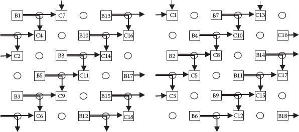
FIGURE 45.8 Subset of a nanofabric in TA-1a and TA-1b.
It can be observed that block B5 is tested in TA-1a and block B4 is tested in TA-1b. Consider the first test architecture TA-1a. The blocks C2, C4, C6, C7, C9, C11, C13, C16, and C18 are configured as comparators and compare the outputs of the BUTs. Initially, all the nanoblocks are assigned a score of “0.”
TABLE 45.1
Pseudocode of the Faculty Block Detection Algorithm
1. Assign a score of zero (0) to all the nanoblocks. 2. For each TA: a. For each comparator: i. If the comparator gives false output, increment score “+1” for each of the corresponding BUTs b. For each BUT: i. If total score is equal to two (2), then the block is marked as defective c. Create the raw defect map. |
Owing to the presence of the faulty block B5, the following comparators would generate a “1” at the output:
• C9: Blocks B3 or B5 have fault F1.
• Increment B3 and B5 by “1.” B3 = 1, B5 = 1.
• C11: Blocks B5 or B8 have fault F1
• Increment B5 and B8 by “1.” B5 = 2, B8 = 1.
The remaining comparisons are successful. Analyzing the above results, the following is obtained:
• B3 = 1
• B5 = 2
• B8 = 1
• Rest of the BUTs = 0
Therefore, eliminating all the blocks with a score of “1” and “0” and only retaining blocks with a score of “2” as faulty blocks, block B5 is diagnosed as faulty and the defect map is updated accordingly. Similarly, the faulty block B4 is identified using test architecture TA-1b. Since the nanoblock size is very large, efficient data structures based on Bloom filters have been proposed for the storage of the defect map [19].
45.3.6 DESIGN OF NEW BUT CONFIGURATIONS AND TEST PATTERNS AND FAULT COVERAGE ANALYSIS
To test the BUTs for defects, we need to configure them internally and apply appropriate test patterns. Configuring a BUT refers to programming of the various cross points in the nanoblock and applying the desired voltages to the nanowires. The BUT configuration and the test pattern target specific fault types. In turn, the particular configuration dictates which pair of complementary test architecture has to be used based on the direction of inputs and outputs. In each configuration, one or more faults can be targeted.
In general, the faults can be divided into two categories: nanowire faults and cross-point faults. The former affects the entire vertical or horizontal wire in nanoblocks, thus rendering it useless. The latter affects only individual cross points and can potentially have no effect on the correctness of a logic function implemented using the remaining good cross points inside the particular block. The configurations are grouped in two sets: (a) Set I that targets the nanowire faults and includes configurations C1 through C4, and (b) Set II that targets the cross-point faults and includes configurations C5 and C6. The following faults are targeted in the next subsection: stuck-at and stuck-open faults, connection faults, and bridging faults using a set of test architectures, BUT configurations, and test patterns.
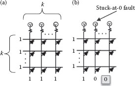
FIGURE 45.9 (a) BUT configurations and test patterns for C1. (b) Example fault detection.
45.3.7 CONFIGURATION C1: STUCK-at-0 AND STUCK-OPEN FAULTS
The BUT configuration C1 is shown in Figure 45.9a. All junctions are programmed as diodes and all inputs are connected to a “1.” Hence, all outputs should be a “1” for a fault-free BUT. However, if any of the lines has a stuck-at-0 and/or stuck-open fault, the corresponding output will be a “0.” Test architectures TA-1a and TA-1b will be used in conjunction with this BUT configuration since the inputs are on the west and outputs on the south of the nanoblock. Consider, for instance, that a vertical line has a stuck-at-0 fault as shown in Figure 45.5b and hence is permanently tied to a 0. As a result, the output for the vertical line 2 will be a “0,” while for all other defect-free lines the output will be a “1” (Figure 45.9).
45.3.8 CONFIGURATION C2: STUCK-at-1 FAULTS
The BUT configuration C2 is shown in Figure 45.10a. All the junctions are programmed to behave as diodes and all inputs are connected to “0.” Hence, for a defect-free BUT, all the outputs should be “0.” However, if any of the lines has a stuck-at-1 fault, the corresponding output will be “1.” Test architectures TA-2a and TA-2b will be used in conjunction with this BUT configuration since the inputs are on the north and outputs on the east of the nanoblock. Consider, for instance, that a vertical line has a stuck-at-1 fault as shown in Figure 45.10b and hence is permanently tied to 1. As a result, the outputs will be “0.”
45.3.9 CONFIGURATION C3: AND/OR BRIDGING FAULTS (h/h)
The bridging faults between adjacent horizontal wires can be detected by using the configuration shown in Figure 45.11a. The BUT is configured in such a way that the programmed diodes are forward-biased. Consider that there is AND bridging between the second and third horizontal wire as shown in Figure 45.11b, and as a result the second horizontal wire is pulled down to a “0”; the output will be inverted. Test architecture TA-1a and TA-1b will be used in conjunction with this BUT configuration.
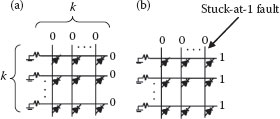
FIGURE 45.10 (a) BUT configurations and test patterns for C2. (b) Example fault detection.
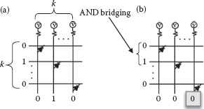
FIGURE 45.11 (a) BUT configurations and test patterns for C3. (b) Example fault detection.
45.3.10 CONFIGURATION C4: AND/OR BRIDGING FAULTS (v/v)
This is similar to the previous configuration, and tests for bridging faults between the vertical wires. The configuration is as shown in Figure 45.12a. The inputs applied and the expected outputs are as shown. However, if there is any AND/OR bridging between the vertical wires, then the output changes. Consider, for example, that the first vertical wire changes to a “1” due to OR bridging with its neighboring wires. This is shown in Figure 45.12b. The diode on that wire will now be reversebiased and hence act as an open switch and the corresponding horizontal output will become a “1.” Test architecture TA-2a and TA-2b will be used in conjunction with this BUT configuration.
45.3.11 CONFIGURATION C5: REVERSE-BIASED DIODE AND v/h BRIDGING FAULTS
All junctions are programmed to behave as diodes. Horizontal wires are connected to a “1” while the vertical wires are connected to a “0” as shown in Figure 45.13a. The output can be taken either from the east side or from the south side. Hence, either of the two test architecture sets can be used. Such a configuration reverse biases all the junction diodes and the outputs are all 1’s if taken on the east side and all 0’s if taken on the south side. In the figure shown, outputs are taken on the east side. If any of the reversed-biased diode is defective and has a small resistance, or there is bridging between the horizontal and vertical wires, the output on the east side will be pulled down to a “0.” This configuration thus detects defective reversed-biased diodes and bridging faults between the vertical and horizontal wires. Consider the example shown in Figure 45.13b. The circled diode is faulty and offers a small resistance in the reverse-biased state. Hence, the corresponding horizontal output changes to a 0.
45.3.12 CONFIGURATION C6: FORWARD-BIASED DIODE FAULTS
For a k × k nanoblock, to detect forward-biased diode faults, we need a total of k configurations to test all the cross points. Figure 45.14a shows these configurations. Here, the vertical wires are connected to Vdd and only one junction is programmed as a diode on each of the horizontal and vertical wires in each configuration. Thus, in the first configuration, we program the cross points in a diagonal fashion. The different subconfigurations are obtained by shifting the programmed cross points one position to the right. The outputs are “0” for a defect-free BUT since the diodes are forward-biased and transmit a “0” to the output. If any of the forward-biased diodes is defective as shown in Figure 45.14b, the corresponding vertical wire output will be pulled up to a “1.” Test architecture TA-1a and TA-1b will be used in conjunction with this BUT configuration.
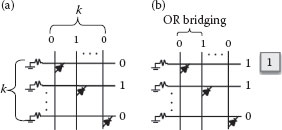
FIGURE 45.12 (a) BUT configurations and test patterns. (b) Example fault detection.
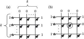
FIGURE 45.13 (a) BUT configurations and test patterns for C5. (b) Example fault detection.
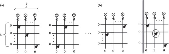
FIGURE 45.14 (a) BUT configurations and test patterns for C6. (b) Example fault detection.
45.3.13 FAULT COVERAGE AND NUMBER OF CONFIGURATIONS
Table 45.2 summarizes the various faults covered using these configurations, and the BUT configuration test architectures to be used for each of the faults. A total of 2k + 10 configurations are needed to the test the entire nanofabric for the given faults. This number is reasonably small compared to other BIST techniques and also provides sufficient fault coverage. Also, it is independent of the number of nanoblocks in a nanofabric. These configurations can be modified as per the optimization technique that is presented in Section 45.4. The optimization technique reduces the number of configurations and/or the number of cross points programmed, thereby reducing the testing time.
TABLE 45.2
Fault Coverage and Configurations
The BUT configurations described above are used to test for one or more faults. Thus, it gives the user a flexibility to choose the configurations depending upon which faults are targeted. Also, each fault detecting configuration will have its own cost associated with it, that is, testing time, complexity, and so on. Table 45.2 can be used to minimize the configurations to be used depending on these factors.
The proposed testing strategy can be optimized such that utilization of the nanoblocks is increased, the testing time reduced, and the number of required configurations decreased. An exhaustive test includes all configurations C1 through C6, where all cross points and nanowires of each nanoblock are tested for all faults. However, it may not be necessary to test all the cross points/NWs in a nanofabric since there are redundant cross points. Consequently, the entire test process includes unnecessary checks and it is possible to test only a subset of cross points and NWs, which are required to implement a logic function. For example, the optimization scheme would select a subset of tests that target only the needed cross points out of all k2 ones. First, we tabulate the list of cross points/NWs tested in each configuration. Next, we remove columns that correspond to the cross points not required by the targeted logic function. Then, using Petrick’s method of reduction, we can obtain the minimal test set required for the targeted faults. In fact, Petrick’s method will list all possible combinations of the tests that are required. Consequently, it is straightforward to assign various weights to performance metrics such as testing time and configuration time, thus enabling a more flexible optimization.
A typical logic implementation in nanoblocks realizes AND and OR gates only [20], since these are the basic gates employed when implementing any logic function. Note that nanoblocks require an external component to implement a NOT logic function, thus complementing the minimal and complete set of gates. Using a k × k nanoblock, we can implement an AND/OR gate with (k − 1) inputs.
Figure 45.2 shows an example of four-input AND/OR gate implemented using 4 × 4 nanoblock. It can be observed that all NWs need to be fault-free. However, only five out of the total sixteen cross points are programmed and take part in implementing the logic function. We will refer to these cross points as effective cross-points. Similarly, for a 4 × 4 nanoblock, to implement a three-input AND/OR gate, there are six effective cross points. In general, for a k × k nanoblock, we can implement a (k − 1) input AND/OR gate, using only 2(k − 1) effective cross points while still needing to test all NWs. The BUT configurations and test patterns described in Section 45.4.2 have been split into two sets—set I that tests the nanowire faults and set II that tests the cross-point faults. Thus, it is possible to optimize the BUT configurations C5 and C6, which belong to set II, in such a way so as to test only the effective cross points.
The performance will be evaluated using the utilization metric, which is a probability that a nanoblock is successfully used to implement a logic function. Considering the effective cross points, the utilization of nanoblocks can be improved since faults in unused cross points will neither be tested nor interfere with correct function implementation. The increase in utilization is due to the fact that we can still use a defective nanoblock to implement a logic function as long as the effective cross points are defect-free.
Consider configuration C5 where all the cross points are tested. This needs to be modified to test only the required cross points. The optimized configuration C5 is shown in Figure 45.15. The entire test targets only the effective cross points based on the assumption that nanoblocks implement only the AND and OR gates. For this, we need to program (k − 1) cross points on one vertical line and (k − 1) cross points on one horizontal line. The number of cross points programmed (and tested) is thus reduced from k2 to 2(k − 1). This reduces a lot of time overhead associated with programming of the cross points and also increases the utilization of the nanoblock.
Now consider the configuration C6 shown in Figure 45.14a where all the cross points are tested. We will demonstrate the optimization using a 3 × 3 nanoblock for simplicity. Three subconfigurations are needed to test all the cross points (for a 3 × 3 nanoblock). We describe two approaches to optimizing C6 and note that each has its own pros and cons.
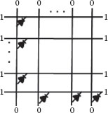
FIGURE 45.15 Customized configuration C5.
45.4.1 ELIMINATION OF REDUNDANT CONFIGURATIONS
It is possible to eliminate the efforts required in designing new configurations to test only the effective cross points by selecting a subset from the defined subconfigurations of C6. Since C6 needs a total of k subconfigurations to test all the cross points, we can lay out a table that lists the different cross points tested in each of the configuration of C6, and then from this table select only the set of configurations that are needed to test the effective cross points. This is demonstrated below in Table 45.3.
Table 45.3 shows the cross points tested in each of the subconfigurations of C6 for a 3 × 3 nanoblock. Here, the assumption is that the nanoblocks are used to implement AND and OR gates only. Hence, from Figure 45.3, we see that there are only four effective cross points—cp11, cp21, cp32, and cp33. From Table 45.3, it can be seen that these four cross points can be tested in two configurations C61 and C63 and the configuration C62 is redundant and can be avoided. Thus, we need only two configurations instead of three as a result of optimization. This can be extended to a k × k nanoblock, wherein the total number of configurations required is now (k−1) instead of k. Moreover, since the number of cross points to be programmed is reduced, this leads to a considerable reduction in testing time.
45.4.2 CUSTOMIZED CONFIGURATIONS
The advantage of the above approach is that there is no need to design new configurations. We can simply select the desired configurations with the help of a table. This is simpler and less time consuming. However, it can be seen in Table 45.3 that, in addition to the effective cross points, some additional cross points are also tested (six cross points in the above case instead of four), which are not required. This reduces the utilization slightly as opposed to the maximum utilization that can be obtained. To have maximum utilization, we can design custom configurations wherein we test only the cross points, which are necessary. Figure 45.16 shows the customized configurations for C6 for a 3 × 3 nanoblock.
TABLE 45.3
Junction Cross Points Tested in Each Configuration
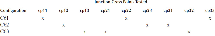
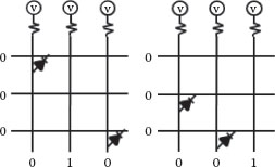
FIGURE 45.16 Customized configuration C6.
Here, again, we need just two configurations but we are testing only the effective cross points. This gives the maximum utilization with a slightly reduced testing time than the first approach. However, this demands that we design new customized configurations and not reuse existing ones.
Once the entire testing phase has been completed and the faulty nanoblocks identified, we can have an additional recovery procedure to diagnose the faulty nanoblocks and further increase the utilization of nanoblocks. This is optional and may be carried out only if utilization is a major concern since this will increase the total testing time.
A defective nanoblock implies that it cannot implement the AND and OR logic within the same nanoblock. However, since the cross points used to implement the AND and OR logic are distinct, we can still have nanoblocks among the defective ones, which can implement either of the two functions but not both. We can have an additional testing phase for the defective nanoblocks to test for the AND or OR implementation. The BUT configurations need to be modified accordingly since we are testing a nanoblock only for one implementation; only the corresponding cross points need to be tested. Thus, at the end of these test phases, we have three sets of usable nanoblocks: (i) those that can be used to implement both the AND and OR functions, (ii) those that can implement only the OR function, and (iii) those capable of implementing only the AND function.
45.5.1 NUMBER OF CONFIGURATIONS/TEST PATTERNS
The BIST approaches developed by the authors in Refs. [16,17] have been discussed in Section 45.2. It can be seen from Table 45.1 that the total number of configurations/test patterns required to test the entire nanofabric is 2k + 10. After using the optimization technique, it results in 2(k−1) + 10. From the analysis of BUT configurations in Section 45.3.3, it can be deduced that only configuration C6 depends on the value of k while the rest of them are independent of k.
We defined the term “nanoblock utilization” as the probability that a nanoblock can be successfully utilized to implement a logic function in the presence of defects. We will derive the expression for nanoblock utilization for the optimized technique and compare it with that of a nonoptimized approach.
Assume a nanoblock of size k × k. Let p be the probability of a faulty cross point. For a nonoptimized testing approach, a nanoblock is deemed as faulty if at least one of its cross points is found to be faulty. Hence, the condition for a nanoblock to be utilized successfully is that all its cross points have to be fault-free.
(45.1) |
For the optimized technique, as described in Section 45.5.1, there are 2(k−1) effective cross points for a k × k nanofabric. For the nanoblock to be successfully utilized to implement the logic function (AND/OR), these 2(k − 1), cross points need to be fault-free. Hence, the utilization in this case is given by:
(45.2) |
The total testing time for the nanofabric can be split into a number of components. Let tconfig denote the total time required to configure the BUT, that is, to program the various cross points and set up power connections. Thus, tconfig would not be the same for all configurations since the number of cross points programmed is not the same for all the configurations.
Let tp denote the time required to program a single cross point and ts be the time required to set up the Vdd/GND connections to the wires. Let ttest denote the time required to apply a test pattern to the BUT, wait for the comparator outputs to be generated, read the comparator outputs, and generate the partial defect map. Here, it is assumed that ttest ≫ tconfig. Using these different components along with the procedure described in Ref. [2], the total time required for testing a nanofabric can be calculated for a k × k nanoblock.
Let Ti denote the testing time for configuration Ci (as described in Section 45.4.2), the testing time for the configuration Ci after using the optimization technique, and the testing time after using the customization approach. The total testing time is given by the sum of the testing times for each of the individual configurations. Summary of improvement in testing times is shown in Table 45.4.
(45.3) |
(45.4) |
(45.5) |
(45.6) |
(45.7) |
(45.8) |
(45.9) |
(45.10) |
(45.11) |
TABLE 45.4
Summary Comparison of the Testing Time
Change due to Optimization |
Change due to Customization |
||
Wire testing time |
C1 |
T1* − T1 = 0 |
T1** − T1 = 0 |
C2 |
T2* − T2 = 0 |
T2** − T2 = 0 |
|
C3 |
T3* − T3 = 0 |
T3** − T3 = 0 |
|
C4 |
T4* − T4 = 0 |
T4** − T4 = 0 |
|
Cross point testing time |
C5 |
T5* − T5 = −2tp[k − 1]2 |
T5** − T5 = −2tp[k − 1]2 |
C6 |
T6* − T6 = − 2[ktp + ttest] |
T6** − T6 = −2k[(k + 2)tp − ttest] |
|
Total difference |
−2[tp(k2 + k − 1) − ttest] |
−2[tp(2k2 − k + 1) − kttest] |
The recovery procedure is discussed in Section 45.4.3. Here, the nanoblock would be usable if it can implement either an AND or OR logic but not both. Though the functionality of the nanoblock is reduced, it is still usable. Hence, we would expect an increase in the utilization of the nanoblock.
If we assume the parameters defined in Section 45.5.2, then the utilization after using the recovery procedure would be given as
(45.12) |
Figure 45.17 shows the comparison between the proposed method and the approaches discussed in Refs. [16,17] with respect to the number of configurations required for testing a k × k nanofabric. The proposed method reduces the number of required configurations over the schemes in Refs. [16,17] since configurations without the effective cross points are eliminated from the test process. Consequently, the testing time for the proposed scheme reduces as shown in the analysis in Section 45.5.
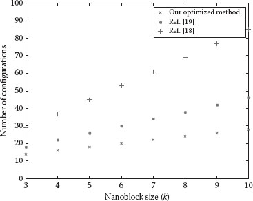
FIGURE 45.17 Number of configurations required in comparison with the approaches discussed in Refs. [18] and [19].
Figure 45.18 shows the plots of (1) and (2) for a value of k between 3 and 10. The optimization technique improves the utilization of the nanoblock since partially defective blocks are not marked as faulty ones, provided the desired logic gates could be correctly implemented.
Figure 45.19 shows the total testing time for a nanoblock size varying between 3 and 10. The improvement in testing time increases with nanoblock size (k) since the fraction of effective cross points to the total number of cross points decreases with the nanoblock size. The number of effective cross points grows linearly with the nanoblock size, while the total number of cross points increases exponentially (k2).
Figure 45.20 shows the plot of (45.12) for a nanoblock size between 3 and 10. The utilization of the nanoblocks improves since the customized configurations target only the effective cross points instead of fewer configurations. Consequently, only defects related to the effective cross points are detected and will mark the block as faulty. This is in contrast to the only optimization technique where unnecessary configurations were removed from the test while still testing the redundant cross points in the remaining configurations. However, since we are testing for partial functionality, we need to carry out additional tests. This results in an increase in the number of tests and testing time. Figure 45.21 shows the increase in testing time as a result of using the recovery procedure. Hence, the improvement in utilization is obtained at the expense of increased testing time. As a result, the recovery procedure should be used only in cases where utilization is more important than testing time.
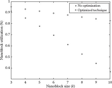
FIGURE 45.18 Improvement in the utilization of the nanoblock.
The novel testing procedure presented, has been shown to outperform the existing testing approaches. The proposed configurations and test patterns provide 100% fault coverage for stuck-at, stuck-open, connection, and bridging faults. The parallel testing architecture does not increase testing time with nanofabric size, thus making it suitable for the dense architectures. Also, it requires only 2k + 10 configurations, which corresponds to 23% reduction over the method discussed in Ref. [16] and 55% reduction over the method proposed in Ref. [17] for a nanoblock size of k = 5. Moreover, using the optimization technique described here, the nanoblock usability is increased from 36% to 76% for nanoblock size k = 5. A significant reduction in the testing time of the nanofabric is also observed. For example, for k = 5, the testing time is reduced by 29%. Moreover, the proposed recovery procedure can tailor testing to a particular functionality (either an AND gate or an OR gate). This further increases the utilization of nanoblocks by 10%. In summary, the proposed technique is simple, efficient, quick, and outperforms the existing approaches. Further work will include theoretical analysis to demonstrate the optimality of the proposed approach, and later the development of a new, fault-tolerant design methodology.
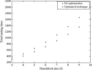
FIGURE 45.19 Total testing time.
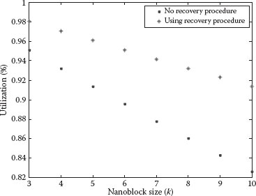
FIGURE 45.20 Improvement in utilization using recovery procedure.
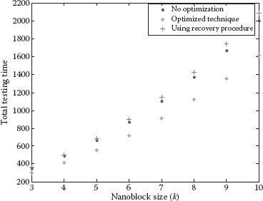
FIGURE 45.21 Increase in testing time as a result of using recovery procedure.
1. S.C. Goldstein and M. Budiu, NanoFabric: Spatial computing using molecular electronics, Proceedings of the International Symposium in Computer Architecture, Victoria, Espírito Santo, Brazil, pp. 178–189, 2001.
2. M. Mishra and S.C. Goldstein, Scalable defect tolerance for molecular electronics, Workshop on Non-Silicon Computing, Cambridge, MA, 2002.
3. S.C. Goldstein and D. Rosewater, What makes a good molecular scale computer device? School of Computer Science, Carneige Mellon University, Tech. Rep. CMU-CS-02-181, September 2002.
4. M. Mishra and S.C. Goldstein, Defect tolerance at the end of the roadmap, Proceedings of the International Test Conference (ITC’03), pp. 1201–1210, 2003.
5. D. Akinwande, S. Yasuda, B. Paul, S. Fujita, G. Close, and H.-S.P. Wong, Monolithic integration of CMOS VLSI and carbon nanotubes for hybrid nanotechnology applications, IEEE Transactions on Nanotechnology, pp. 636–639, 2008.
6. R.M.P. Rad and M. Tehranipoor, A reconfiguration-based defect tolerance method for nanoscale devices, 21st IEEE International Symposium on Defect and Fault Tolerance in VLSI Systems, DFT ‘06, Washington DC, pp. 107–118, 2006.
7. D. Jianwei, W. Lei, and J. Faquir, Analysis of defect tolerance in molecular crossbar electronics, IEEE Transactions on Very Large Scale Integration (VLSI) Systems, pp. 529–540, 2009.
8. A.A. Al-Yamani, S. Ramsundar, and D.K. Pradhan, A defect tolerance scheme for nanotechnology circuits, IEEE Transactions on Circuits and Systems I: Regular Papers, pp. 2402–2409, 2007.
9. J.G. Brown and R.D.S. Blanton, CAEN-BIST: Testing the nanofabric, Proceedings of the International Test Conference, Charlotte, NC, pp. 462–471, 2004.
10. C. Stroud, S. Konala, P. Chen, and M. Abramivici, Built-in self-test of logic blocks in FPGAs (finally, a free lunch: BIST WithoutOverhead), Proceedings of the IEEE VLSI Test Symposium (VTS’96), Princeton, NJ, pp. 387–392, 1996.
11. M.B. Tahoori, E.J. McCluskey, M. Renovel, and P. Faure, A multi-configuration strategy for an application dependent testing of FPGAs, Proceedings of IEEE VLSI Test Symposium (VTS’04), Napa Valey, CA, pp. 154–159, 2004.
12. C. Metra, G. Mojoli, S. Pastore, D. Salvi, and G. Sechi, Novel technique for testing FPGAs, Proceedings of Design, Automation and Test in Europe (DATE’98), Paris, France, pp. 89–94, 1998.
13. S.J. Wang and T.M. Tsai, Test and diagnosis of faulty logic blocks in FPGAs, IEE Proceedings: Computers and Digital Techniques, Kwangju, South Korea, pp. 100–106, 1999.
14. S. Kundaikar and M. Zawodniok, Optimized built-in self-test technique for CAEN-based nanofabric systems, Proceedings of 11th IEEE Conference on Nanotechnology (IEEE-NANO’11), Portland, OR, pp. 1717–1722, 2011.
15. M. Tahoori, Application-dependent diagnosis of FPGAs, Proceedings of the International Test Conference (ITC’04), Charlotte, NC, pp. 645–654, 2004.
16. Z. Wang and K. Chakrabarty, Built-in self-test of molecular electronics-based nanofabrics, European Test Symposium, Tallinn, Estonia, pp. 168–173, 2005.
17. M. Tehranipoor, Defect tolerance for molecular electronics-based NanoFabrics using built-in self-test procedure, 20th IEEE International Symposium on Defect and Fault Tolerance in VLSI Systems (DFT), Monterey, CA, 2005.
18. M.V. Joshi and W.K. Al-Assadi, A BIST approach for configurable nanofabric arrays, 8th IEEE Conference on Nanotechnology, Arlington, TX, pp. 695–698, 2008.
19. G. Wang, On the use of Bloom filters for defect maps in nanocomputing, Proceedings of ICCAD 2006, San Jose, CA pp. 743–746, 2006.
20. M. Abramovici, E. Lee, and C. Stroud, BIST-based diagnostics for FPGA logic blocks, Proceedings of the International Test Conference, Washington, DC, pp. 539–547, 1997.