
Adaptive Fault-Tolerant Architecture for Unreliable Device Technologies |
CONTENTS
46.3 The Adaptive Averaging Cell
46.4 Comparison: Balanced versus Unbalanced AVG
46.5 AD–AVG Technology Implementation
Computer architecture constitutes one of the key and strategic application fields for new, emerging devices at nanoscale dimensions, potentially getting benefit from the expected high-component density and speed. However, these future technologies are expected to suffer from a reduced device quality, exhibiting a high level of process and environmental variations as well as performance degradation due to the high stress of materials [1, 2, 3 and 4]. This clearly indicates that if we are to make use of those novel devices, we have to rely on fault-tolerant architectures. Currently, most of the redundancy-based fault-tolerant architectures make use of majority gates (MAJ) [5,6] and require high area overhead. An alternative to majority gate voting is the averaging cell (AVG) [7, 8 and 9], which can exhibit higher reliability at a lower cost. The underlying principle of the AVG is to average several input replicas in order to compute the most probable output value. This approach is quite effective in case the AVG inputs are subject to independent drifts with the same/similar magnitude. In practice, however, input deviations can be nonhomogeneous, in which case the balanced average cannot provide a response that minimizes the output error probability.
To alleviate this problem, we propose the adaptive average cell (AD–AVG) [10], which is able to better cope with nonhomogeneous input drifts. This technique uses the principle of nonparity voting and gives more weight to the inputs that are known to be more reliable to the detriment of the less reliable ones. This unbalanced voting is performed by adjusting the relative magnitudes of each average weight.
In Section 46.2, we present the AVG architecture and its main features, and we obtain the equation to calculate the output error probability. In Section 46.3, we introduce the idea of unbalanced voting with the AD–AVG technique and demonstrate that it is possible to optimize the values of the average weights in order to minimize the output error probability. We also find the analytic expression of the optimal weights. In Section 46.4, we present the results of Monte Carlo simulations of the AVG structure with balanced and optimal unbalanced weights and compare the behavior of both approaches in the presence of the heterogeneous variability levels in the input replicas. Our experiments indicate that the proposed method of optimal unbalanced weights is more robust against degradation effects and external aggressions, and that for the same reliability level it requires a lower redundancy level (less area overhead). In Section 46.5, we propose a technology implementation for the AD–AVG structure based on switching resistance crossbars and explore its behavior by means of Monte Carlo simulations. Finally, we present the conclusions.
The averaging cell (AVG), widely known for its application in the four-layer reliable hardware architecture (4LRA) [9], stems from the perceptron, the McCulloch–Pitts neuron model [11,12]. Associated with fault-tolerant techniques based on redundancy, the AVG graphically depicted in Figure 46.1 can calculate the most probable value of a binary variable from a set of error-prone physical replicas. While the MAJ-based voting technique operates in the digital domain, the AVG performs a weighted average of the replicated inputs in the analog domain. There are R physical replicas of an ideal variable y:
(46.1) |
Each of the input replicas yi has associated an independent drift ηi that modifies its ideal value y. As a consequence, input signals yi are observed in the system as continuous voltage levels, where 0 and Vcc stand for ideal logical values “0” and “1,” respectively. The output of the AVG ŷ is an estimation of y according to (46.2) and (46.3).
(46.2) |
(46.3) |
To simplify the mathematical formulation, we use the normalized weights instead of weights ki, i = 1, …, R. We model the drift magnitudes ηi as Gaussian random variables with a null mean and a standard deviation σi, ηi ~ N(0, σi)
When y′ is processed by the threshold operation T(y′), an error is produced if and only if the deviation in the weighted average ϵ = y′ − y reaches Vcc/2 or −Vcc/2, depending on the ideal logic value y. Since this deviation parameter ε can be expressed as a linear combination of normally distributed variables ηi, by the properties of the normal distribution, the probability density function (PDF) fϵ (ϵ) can be described as a normal distribution with parameters:
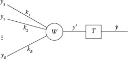
FIGURE 46.1 Averaging cell (AVG) architecture. (N. Aymerich et al. Adaptive fault-tolerant architecture for unreliable device technologies, 11th IEEE International Conference on Nanotechnology, Portland, Oregon, pp. 1441–1444 © (2011) IEEE. With permission.)
(46.4) |
(46.5) |
Thus, using the complementary Gauss error function, we can formulate analytically the output error probability as Equation 46.6. Figure 46.2 depicts the relationship between σy′ and Pe and its monotonically increasing behavior. Thus, given a requirement of output error probability Pe, there is a maximum admissible output standard deviation σy′. For example, an output error probability of Pe <2 × 10⁻⁴ implies having an output standard deviation lower than σy′ < 0 14. V.
(46.6) |
A previous AVG-based study assumes homogeneous input drifts [8], a case in which a balanced weight set produces a weighted average y′ with a minimum standard deviation σy′, and therefore the output error probability Pe is minimized. However, when the input drifts lose homogeneity due to aging and variability effects, the output standard deviation increases and so does the output error probability Pe. Under these conditions, the error probability Pe becomes highly dependent on the level of heterogeneity. In the next sections, we make use of the fact that the replica weights can be different and introduce a method to compute them in such a way that Pe is minimized even under severe nonhomogeneous aging and variability conditions.
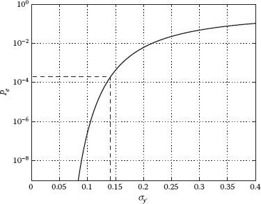
FIGURE 46.2 Output error probability Pe against the output standard deviation σy′. The relationship is monotonically increasing; thus, Pe < 2 × 10⁻⁴ implies having an output standard deviation lower than σ y′ < 0 14.V. (N. Aymerich, S. Cotofana, and A. Rubio. Adaptive fault-tolerant architecture for unreliable device technologies, 11th IEEE International Conference on Nanotechnology, Portland, Oregon, pp. 1441–1444 © (2011) IEEE. With permission.)
46.3 THE ADAPTIVE AVERAGING CELL
The AVG provides robustness when all the inputs are under the same aggression factors, in which case balanced weights provide the best drift compensation. However, in practice, this may not be the case, as some replicas may have a larger drift with respect to others. As a consequence, owing to this decompensation, the balanced weights approach becomes suboptimal. In this section, while preserving the AVG architecture, we consider the nonhomogeneity of the aggression factors and degradation effects. We propose to adjust the AVG weighting scheme according to the following principle: assign greater weight to the less degraded and more reliable inputs, and lower weight to the ones that are more prone to be unreliable. Inductively speaking, such an approach should improve the overall reliability.
Before the calculation of the optimal set of weights, we demonstrate that it always exists regardless of the environmental variability conditions. To show this, we analyze the sensitivity of the error probability Pe against the variation of one specific weight cj. We show that there is always a minimum in the error probability and thus an optimal value for the weight cj. For the analysis, we assume different levels of variability in the input j modeled with the parameter σj ranging from 0 to 0.4 V. The rest of the inputs are considered all together with a fixed contribution to the variability modeled by the standard deviation parameter . In these conditions, taking into account that increasing the weight cj implies decreasing the rest of the weights, according to the restriction , the variance of the weighted average can be expressed as Using this result and substituting into Equation 46.6, we can analyze the influence of cj on the error probability Pe. Figure 46.3 depicts the error probability against the weight cj for different levels of input variability. One can observe the different locations of the Pe minimum and the relation between optimal weights and different levels of variability.
The following comments can be extracted from Figure 46.3:
• There is always one and only one value of weight cj in the range from 0 to 1 that minimizes the error probability Pe in each possible variability environment.
• The optimal value of weight cj is never exactly equal to 0. Even for large levels of deviation in the jth input with respect to the others, it is useful to have a contribution from the input j.
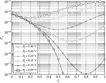
FIGURE 46.3 Variation of the error probability Pe against the weight cj. Standard deviation in the input j ranges from σj = 0V to σj = 0.4V and the standard deviation of the weighted average due to the rest of the inputs is . (N. Aymerich, S. Cotofana, and A. Rubio. Adaptive fault-tolerant architecture for unreliable device technologies, 11th IEEE International Conference on Nanotechnology, Portland, Oregon, pp. 1441–1444 © (2011) IEEE. With permission.)
• The optimal value of weight cj is never exactly equal to 1. Even for small levels of deviation in the jth input with respect to the others, it is useful to have a contribution from the rest of the inputs.
• Based on one’s intuition, in order to minimize the output error probability Pe, higher weights (close to 1) should be assigned to less deviating inputs and vice versa.
• When the deviating effect in the input j (σj) is equal to the deviating effect of the rest of the inputs , the optimal value for the weight cj is one-half. Note that in Figure 46.3 the curve with minimum at
The set of weights that minimizes the output error probability Pe can be found analytically by minimizing the standard deviation of the weighted average σy′; this magnitude is directly related to Pe as Equation 46.6 evidences. In order to perform this minimization considering all the weights ci simultaneously, we make use of the Lagrange multipliers as there is an additional restriction to be held for the weights. The target function to minimize is the standard deviation of the weighted average σy′, or equivalently the variance , and the variables are the magnitudes of the averaging weights cj. The condition to be held is the restriction normalized weights . Therefore, the target function is
(46.7) |
Differentiating with respect to the normalized weights cj, recall Equation 46.5, and Lagrange multiplier λ and equating to zero to find the minimum, we obtain the following equations:
(46.8) |
(46.9) |
Equation 46.8 shows that the optimal weights are inversely proportional to the input variances and Equation 46.9 expresses the condition of normalized weights. Combining both conditions, we deduce the value of A:
(46.10) |
Now, we can calculate the explicit formula for the optimal weights. It depends only on the input variances :
(46.11) |
This is the optimal configuration of weights that minimizes the error probability Pe. Depending on the input drifts distribution, each weight should be tuned according to Equation 46.11 in order to achieve the lowest possible output error probability Pe. We can observe how the optimal weights are small when the input variance is large and vice versa. We can also calculate the value of the standard deviation σy′ when we apply optimal weights; this value is the minimum of σy′ and coincides with A (σy′ min =A). So it is also possible to express each optimal weight in terms of its input variance and the minimum variance of the weighted average:
(46.12) |
The optimal configuration has all the weights directly proportional to the constant and inversely proportional to its input variance . A further comment can be made regarding the analytical expression of the optimal weights: the particular case in which one or more inputs have null variability σi = 0 has to be treated separately. First, we have to say that in practice this situation will never happen because there is always at least a small contribution of noise that affects all the input signals. However, if this case occurs, then the minimization of the output error probability would be straightforward: assigning the maximum weight to the input with null variability ci = 1, we would obtain a null output error probability Pe = 0, see Equations 46.5 and 46.6.
46.4 COMPARISON: BALANCED VERSUS UNBALANCED AVG
To assess the implications of our proposal, we carried out a reliability analysis for the AVG with balanced and optimal unbalanced weights. Given a nonuniform input drift scenario, we calculated the percentage of circuits that achieve an output error probability Pe lower than 2 × 10⁻⁴ (equivalently σy′ < 0.14 V). We used this condition as criteria to define the yield of the AVG circuit. In the simulation, in order to reproduce realistic heterogeneous environments, the per replica drift variances were generated with a chi-square distribution We modeled the effect of degradation using different mean values for the drift distribution σm. In the experiment, we used two levels: the first one corresponding to less degraded environments (σm = 0.6 V) and the second one reproducing more degraded environments (σm = 0.8 V). Using Monte Carlo computation, we estimated for both approaches (balanced and unbalanced weights) the yield of circuits. Figure 46.4 presents the results against the redundancy level R. One can observe in the figure that the AVG with unbalanced weights can deliver the same yield with a much lower redundancy factor R. For example, if we require a 90% yield in a technology with a level of heterogeneity that can be modeled with a chi-square distribution with σm between 0.6 and 0.8 V, the use of optimal unbalanced weights can save from 70% to 77% of redundancy level R with respect to the balanced approach.
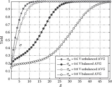
FIGURE 46.4 Percentage of AVG circuits that accomplish Pe < 2 × 10⁻⁴ against the redundancy level R at different levels of heterogeneous variability. Circle markers correspond to the conventional AVG and square markers correspond to the optimal unbalanced AVG approach. (N. Aymerich, S. Cotofana, and A. Rubio. Adaptive fault-tolerant architecture for unreliable device technologies, 11th IEEE International Conference on Nanotechnology, Portland, Oregon, pp. 1441–1444 © (2011) IEEE. With permission.)
Thus, we demonstrated that if we knew the distribution of deviations among the replicas, we could design better devices at lower cost. The capability of adjusting the average weights in the AVG structure provides a way to counteract the nonhomogeneous variability effects of degradation and external aggressions.
46.5 AD–AVG TECHNOLOGY IMPLEMENTATION
In this section, we propose a realistic technology implementation for the presented AD–AVG structure. This implementation is based on the use of switching resistance crossbars. In order to efficiently modify the configuration of weights as required by the structure and follow the changes of the input variability levels to maximize the AD–AVG reliability, we need a technology implementation with high reconfiguration capabilities. In this sense, the use of crossbars of resistive switching devices provides the required framework, such as memristor crossbars [14,15].
Figure 46.5 depicts the AD–AVG structure implementation using a switching resistance crossbar, a threshold block, a variability monitor, and a set of weight drivers. The complete architecture can be decomposed into three layers. The first one corresponds to the input layer and receives the input signals from the replicas. The second layer performs the averaging operation by means of the resistive switching crossbar configured taking into account the information provided by the variability monitor. The third one corresponds to the decision layer; it restores the binary output value by means of a threshold function.
In the following, we analyze the practical repercussions of implementing the proposed AD–AVG structure by means of resistive switching crossbars. The basic idea of implementing different averaging weights for each input is to connect or disconnect more or less devices in the corresponding input line. Figure 46.6 reproduces a detailed view of the resistive switching crossbar layout used to implement the averaging weights. Each of the inputs is connected to a horizontal metal line that can be connected or disconnected to N vertical lines. There is one resistive switching device situated in each crossing point of the crossbar to connect or disconnect the lines. In Figure 46.6, black dots correspond to the connected devices. The state of each device can be easily controlled with the weight drivers applying specific configuration voltages to each vertical and horizontal line.
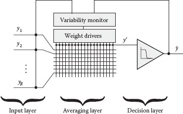
FIGURE 46.5 Adaptive averaging cell (AD–AVG) implementation in switching resistive crossbar technology.
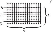
FIGURE 46.6 Crossbar layout view of the AD–AVG to configure the averaging weights.
Figure 46.6 shows that the output line, corresponding to the signal y′, is connected to all the vertical lines, whereas the horizontal lines have a different number of connections. Using this feature, we can set up a network of interconnects that averages the input replicas with specific averaging weights. The resistive switching devices exhibit a different resistance depending on the state (RON and ROFF). For example, in the case of memristors, the values of resistances are: RON ≈ 1MΩ and ROFF ≈ 1GΩ. Analyzing the equivalent circuit, we can calculate the analytic expression of signal y′ in terms of the inputs yi and the crossbar configuration of connections ni, i = 1,…,R, see Equation 46.13. The ni values correspond to the number of devices connected in the input line i. This result allows us to deduce the particular value of the averaging weights in terms of parameters ni.
(46.13) |
In the following, we perform an experiment to prove the behavior of the proposed implementation. We simulate a 2-input AD–AVG implemented in a switching resistance crossbar with N = 20 vertical lines. We analyze the impact of the connecting and disconnecting devices in the structure against different levels of variability in the inputs. To perform this experiment, we run 1000 Monte Carlo simulations of the structure and find the AD–AVG yield for each possible configuration (from 0 to N devices connected in both input lines). Figure 46.7 reproduces the simulation result of the yield against the connected devices and for a homogeneous input variability level with σ = 0.15 V. We confirm that the yield is maximized when n1 is equal to n2, as expected. The homogeneity in the variability levels implies a symmetric optimal configuration of weights. However, we also observe that the larger the number of connected devices, the wider is the region with a high yield. This is an interesting result as it means that if we have difficulties in obtaining the exact value of variability in the inputs, we can look for configurations with a large number of connected devices to reduce the impact of nonperfect determination of the optimal averaging weights.
The second part of the experiment corresponds to the simulation of the same structure with a nonhomogeneous environment of variability with σ1 = 0.13 V and σ2 = 0.17 V. Figure 46.8 shows the simulation result for the yield of the 2-input AD–AVG. In this case, we observe that the maximum yield condition is not n1 = n2. As the input variability levels are different, the optimal weights are not balanced. Using the result (46.12), we can calculate c1/c2 as ; this yields the condition . Applying now the result (46.13), we get the condition required for the optimal averaging weights: . If we assign the maximum possible value to n1 = 20, then the optimal n2 value is n2 = 12, which is coherent with the simulation in Figure 46.8.
With this result, we prove that by using the proposed implementation for the AD–AVG it is easy to determine and configure the number of connections that we need in each input line to maximize the reliability. We just need a good estimation of the input levels of variability. Our simulation results correspond to a particular case of the 2-input AD–AVG structure, but the mechanism can be easily extended to structures with more input replicas by distributing the crossbar connections among a larger number of input replicas.
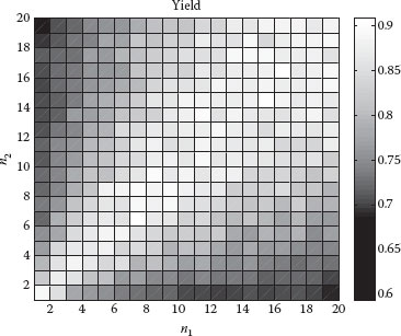
FIGURE 46.7 A 2-input AD–AVG yield against the connected devices in the input line 1 (n1) and line 2 (n2) for a homogeneous level of variability in the inputs with σ = 0.15 V.
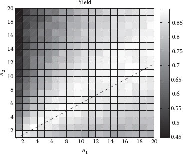
FIGURE 46.8 A 2-input AD–AVG yield against the connected devices in the input line 1 (n1) and line 2 (n2) for a nonhomogeneous variability level in the inputs with σ1 = 0.13V and σ2 = 0.17V. The dashed line corresponds to the optimal condition of the parameters n1 and n2 to maximize the yield .
In this section, we introduce an adaptive averaging cell (AD–AVG) structure tailored for realistic environments with nonhomogeneous variability. We demonstrate the efficiency of using adjustable weights in the averaging cell structure taking into account the heterogeneous variability levels among the replicas. We provide a method to calculate the optimal weights to minimize the output error probability and find that these values are inversely proportional to the input variances. The simulation of the AD–AVG technique indicates that it potentially results in substantial reliability improvement, at a lower cost than other equivalent state-of-the-art methods. A 70% reduction of the redundancy overhead has been found for realistic, nonhomogeneous scenarios with a chi-square distribution of input drift variances. We also propose a technology implementation based on the use of switching resistance crossbars and simulate its behavior, proving that it is possible to establish an adaptive mechanism to maximize the AD–AVG reliability according to the particular nonhomogeneous variability conditions.
1. M. Mishra and S. Goldstein, Scalable defect tolerance for molecular electronics, in First Workshop on Non-Silicon Computing. Citeseer.
2. S. Borkar, T. Karnik, S. Narendra, J. Tschanz, A. Keshavarzi, and V. De, Parameter variations and impact on circuits and microarchitecture, in Proceedings of the 40th Annual Design Automation Conference. ACM, 2003, pp. 338–342.
3. S. Borkar, Electronics beyond nano-scale CMOS, in Proceedings of the 43rd Annual Design Automation Conference. ACM, 2006, pp. 807–808.
4. S. Borkar, Designing reliable systems from unreliable components: The challenges of transistor variability and degradation, IEEE Micro, 25(6), 10–16, 2005.
5. M. Stanisavljevic, A. Schmid, and Y. Leblebici, Optimization of nanoelectronic systems’ reliability under massive defect density using cascaded R-fold modular redundancy, Nanotechnology, 19, 4065202, 2008.
6. M. Stanisavljevic, A. Schmid, and Y. Leblebici, Optimization of nanoelectronic systems reliability under massive defect density using distributed R-fold modular Redundancy (DRMR), in Defect and Fault Tolerance in VLSI Systems, 2009. DFT’09. 24th IEEE International Symposium on. IEEE, 2009, pp. 340–348.
7. A. Schmid and Y. Leblebici, Robust circuit and system design methodologies for nanometer-scale devices and single-electron transistors, IEEE Transactions on Very Large Scale Integration(VLSI) Systems, 12(11), 1156–1166, 2004.
8. F. Martorell, S. Cotofana, and A. Rubio, An analysis of internal parameter variations effects on nanoscaled gates, IEEE Transactions on Nanotechnology, 7(1), 24–33, 2008.
9. M. Stanisavljevic, A. Schmid, and Y. Leblebici, Optimization of the averaging reliability technique using low redundancy factors for nanoscale technologies, Nanotechnology, IEEE Transactions on, 8(3), 379–390, 2009.
10. N. Aymerich, S. Cotofana, and A. Rubio. Adaptive fault-tolerant architecture for unreliable technologies with heterogeneous variability, IEEE Transactions on Nanotechnology, 11(4), 818–829, July 2012.
11. W. S. McCulloch and W. Pitts, A logical calculus of the ideas immanent in nervous activity, Bulletin of Mathematical Biophysics 5, 115–133 (Reprinted in Neurocomputing Foundations of Research Edited by J.A. Anderson and E. Rosenfeld, the MIT Press, 1988), 1943.
12. W. Pitts and W. S. McCulloch, How we know universals: The perception of auditory and visual forms, Bulletin of Mathematical Biophysics 9, 127–147 (Reprinted in Neurocomputing Foundations of Research Edited by J.A. Anderson and E. Rosenfeld, the MIT Press, 1988), 1947.
13. N. Aymerich, S. Cotofana, and A. Rubio. Adaptive fault-tolerant architecture for unreliable device technologies, 11th IEEE International Conference on Nanotechnology, Portland, Oregon, pp. 1441–1444, 2011.
14. G. Snider, Computing with hysteretic resistor crossbars, Applied Physics A, 80(6), 1165–1172, Mar 2005.
15. J. Borghetti, Z. Li, J. Straznicky, X. Li, D. Ohlberg, W. Wu, D. Stewart, and R. Williams, A hybrid nanomemristor/transistor logic circuit capable of self-programming, Proceedings of the National Academy of Sciences, 106(6), 1699–1703, Feb 2009.