
Growth and Characterization of GaAs Nanowires Grown on Si Substrates |
CONTENTS
47.2 Growth of III–V Nanowires on Silicon Substrates
47.2.1 Morphology of III–V Nanowires Grown on Si (111) Substrates
47.2.2 Crystal Structure of GaAs Nanowires Grown on Si (111) Substrates
47.4 Morphology Improvement of GaAs Nanowires by Thin Buffer Layers
47.4.1 Growth of Thin GaAs Buffer Layers on Si (111) Substrates
47.4.2 Morphology of GaAs Nanowires Grown on Si (111) Substrates Coated with Buffer Layers
47.5 Improvement of Crystal Structure of III–V Nanowires
47.6 Optical Properties of Nanowires for Device Applications
Recently, nanowires (NWs) have come into the spotlight for future integrated optoelectronic devices. III–V compound semiconductor NWs are unique, in that they can be grown epitaxially on Si substrates, which allow the integration of III–V-based optoelectronics with established Si microelectronics technologies [1, 2 and 3]. That is to say, well-aligned NW morphology with vertical growth is a rudimentary necessity in the applications of III–V compound semiconductor NWs on Si substrates. However, several problems must be overcome to obtain the successful integration of III–V compound semiconductors with Si [4,5], including lattice and thermal expansion mismatch, and the formation of antiphase domains. For the case of Si, in particular, the existence of a native oxide layer at the interface between NWs and substrates is a major factor preventing the epitaxial growth of NWs [1]. To achieve nanoscale optoelectronic devices, it is also crucial to fabricate NWs with a high-quality crystal structure and controllable composition. For optoelectronic device applications, NW defects such as twin defects, phase polytypism, and stacking faults may give rise to the deterioration of optical and carrier transport properties and are therefore undesirable [6]. Overcoming these issues, namely, the interface defects between NWs and substrates and crystal structure defects, is the first priority to obtain perfect III–V compound semiconductor NWs on Si substrates for nanoelectronic device applications.
47.2 GROWTH OF III–V NANOWIRES ON SILICON SUBSTRATES
47.2.1 MORPHOLOGY OF III–V NANOWIRES GROWN ON SI (111) SUBSTRATES
Generally, III–V NWs grown on Si substrates without any special treatments have messy and randomly oriented morphology as shown by scanning electron microscopy (SEM) images in Figure 47.1. Here, GaAs NWs (Figure 47.1a), InP NWs (Figure 47.1b), and GaP NWs (Figure 47.1c) were grown on HF-etched Si (111) substrates using Au catalysts by metal–organic chemical vapor deposition (MOCVD). This messy morphology has resulted from the nonepitaxial growth of the NWs on the Si substrates, possibly due to the native oxide layer and interface defects.
In terms of the general planar growth of III–V semiconductor materials on Si, a high density of defects is the result due to their mismatch in lattice parameters and thermal expansion coefficients, and naturally, NWs are no exception. Owing to these mismatches, lattice expansion or contraction can take place by stressing its bonds in the growth direction, which will result in the formation of crystal defects at the interface between III–V and Si, once the so-called pseudomorphic growth regime is exceeded [7]. “Antiphase domain formation” arises during the growth of polar materials (III–V semiconductors) on nonpolar materials (Si). In terms of GaAs NWs on Si, for instance, silicon has a diamond crystal structure with homogeneous two-fcc sublattices (only Si atoms). However, GaAs has a zinc blende (ZB) structure, where the Ga and As atoms occupy a sublattice each. Therefore, the interface between the GaAs epilayer and Si substrates will have a defective boundary with the antiphase domains consisting of Ga–Ga and As–As bonding. In addition, the existence of an amorphous native oxide layer at the Si surface is a decisive factor to prevent the epitaxial growth of high-quality material on silicon [8].
Even though there are a few reports of epitaxial growth of straight and vertical III–V NWs on Si substrates [8, 9 and 10], it is still a major challenge to prepare the surface properties of Si suitable for NW nucleation, such as substrate etching and cleaning, baking, and specific growth temperature. A simpler and easily reproducible approach is highly desirable to achieve epitaxial growth of III–V NWs on Si.
47.2.2 CRYSTAL STRUCTURE OF GAAS NANOWIRES GROWN ON SI (111) SUBSTRATES
A typical morphology of GaAs NWs grown directly on Si was shown in Figure 47.2a, which has a tapered shape and a serrated sidewall. The transmission electron microscopy (TEM) image (Figure 47.2b) shows a high density of stacking faults (the dark bands) in this NW and a sawtooth-like facet. The high-resolution (HR) TEM image of Figure 47.2c clearly shows the ZB structure with a thin twin plane. In fact, this type of twin defects is commonly associated with the sidewall faceting behavior of ZB III–V compound NWs [11, 12 and 13]. Generally, faceting takes place in association with the high density of twins at high growth temperatures [12,14].
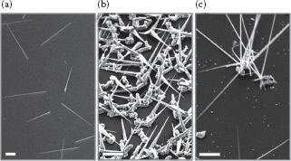
FIGURE 47.1 SEM images of (a) GaAs NWs, (b) InP NWs, and (c) GaP NWs on Si (111) substrate; scale bars are 2 μm.
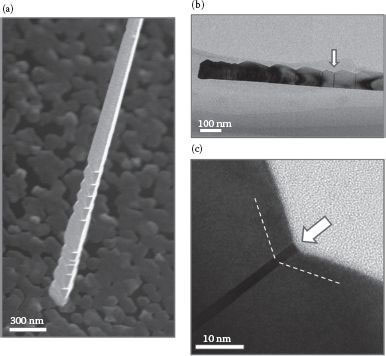
FIGURE 47.2 (a) A SEM image (45° tilted) of single GaAs NW on Si (111) substrates, (b) a TEM image of the NW showing sawtooth-like facets with many segments, and (c) a HR-TEM image illustrating a twin defect at one of the segments (arrow).
To achieve efficient nanoscale optoelectronic devices, an overall improvement is necessary in the morphology and crystal structure.
In this study, the GaAs layers and NWs were grown on Si substrates by horizontal-flow low-pressure MOCVD. Au particles of 50 nm were used as catalysts via the vapor-liquid-solid (VLS) mechanism for NW growth and the substrates used here were the Si substrates having (111) orientation with 4°-miscut toward the (112) direction. Trimethylgallium (TMGa) and arsine (AsH3) were used as the group III and V precursor source materials, respectively, and the reactor pressure was fixed at 100 mbar.
To improve the morphology of the NWs, buffer layer growth was introduced first. The Si substrates were etched with 4.8% diluted hydrofluoric (HF) solution to remove the native oxide layer prior to buffer growth. Three types of buffer layer structures were investigated. For a single buffer layer structure, only one GaAs layer was grown on Si substrates at 400°C for 1 h with a low V/III ratio of 15.4 (structure No. 1). This single buffer layer also acts as the initial layer in the double buffer layer structure, where the subsequent GaAs buffer layer was grown at 700°C for 10 min with a higher V/III ratio of 154.3 without growth interruption during the heating up step from 400°C to 700°C (structure No. 2). After the deposition of the second GaAs buffer layer, selected samples were annealed in situ at 750°C for 15 min under AsH3 atmosphere to prevent desorption of As from the GaAs buffer layers (structure No. 3).
For NW growth, the Si substrates coated with a GaAs buffer were treated by poly-L-lysine (PLL) the solution (to attach Au particles) and then the Au particles were dispersed onto the surface. After all treatments were finished, the sample was annealed again at 600°C for 10 min under the AsH3 ambient to remove contamination and form the eutectic alloys. Three different GaAs NWs were grown at temperatures of 375 ~ 450°C for 6 or 30 min with different precursor flow rates. More details of the growth conditions of each sample will be given later as required. After the growth of GaAs NWs, AlGaAs shell growth was performed at 650°C for 20 min with an Al vapor concentration of 26% and the same flows of TMGa and AsH3 as described above. The AlGaAs shell was finally covered by a thin GaAs cap grown for 5 min at the same temperature to prevent oxidation.
47.4 MORPHOLOGY IMPROVEMENT OF GAAS NANOWIRES BY THIN BUFFER LAYERS
47.4.1 GROWTH OF thin GAAS BUFFER LAYERS ON SI (111) SUBSTRATES
Figures 47.3 shows the illustrations, SEM, and TEM images of the three different types of GaAs buffer layers. The single buffer layer grown on Si (111) substrates at a low temperature (400°C) with a low V/III ratio (15.4) as shown in Figure 47.3a has a rough surface as seen in the SEM image. We speculate that, during growth, islands initially build up due to the lattice mismatch between the Si substrate and the growing GaAs material [15,16] until finally the layer forms a polycrystalline structure made up of the coalescence of these small islands. The HR-TEM image of the single buffer layer illustrates that abundant structural defects exist in this thin buffer layer (~12 nm), such as dislocations and stacking faults, with surface irregularity. The poor crystalline quality of this single buffer layer indicates that this layer is unsuitable for the subsequent growth of NWs.
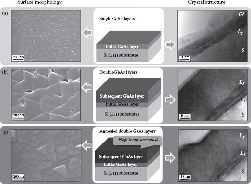
FIGURE 47.3 SEM images, pictorial illustrations, and cross-sectional TEM images of the three types of GaAs buffer layers grown on Si (111) substrates: (a) a single buffer layer, (b) double buffer layers, and (c) annealed double buffer layers, respectively (S: Si substrate, LI: the initial/single GaAs buffer layer, LS: the subsequent GaAs buffer layer, and G*: amorphous glue used during sample preparation).
The double GaAs buffer layer structure consists of an initial layer that is the same as a single buffer layer and the subsequent layer grown at a high temperature (700°C) with a high V/III ratio (154). The SEM image in Figure 47.3b shows the surface with triangular terraces and the occasional presence of voids. The triangular symmetry of the crystals is related to the ZB structure of GaAs grown on the (111) surface. The TEM image taken from the [110] zone axis shows that the upper region of the GaAs layer is almost free of lattice defects and superior to the single buffer layer.
In situ annealing at high temperature (750°C) effectively improves the surface morphology of the double buffer layer structure as seen in the SEM image of Figure 47.3c. The triangular terraces have become smoother and the surface voids have also disappeared due to recrystallization. The TEM image also shows a dislocation-free upper GaAs layer and the lattice defects in the initial layer are also reduced after annealing.
47.4.2 MORPHOLOGY OF GAAS NANOWIRES GROWN ON SI (111) SUBSTRATES COATED WITH BUFFER LAYERS
SEM images in Figure 47.4 show the morphology of the GaAs NWs grown on the Si (111) substrates directly and coated with various GaAs buffer layers explained earlier. The growth conditions for all NWs are the same: growth temperature, growth time, and V/III ratio were 450°C, 30 min, and 46.3, respectively. In all cases, except the direct growth of GaAs NWs on Si substrates, most GaAs NWs grow vertically along the [111] direction, indicating the epitaxial relationship of NWs with the buffer layers and substrates. A typical morphology of GaAs NWs grown directly on an Si (111) substrate is shown in Figure 47.4a, where a very low density of NWs was observed and found to exhibit a random growth direction. Although HF etching was used to remove the native oxide on the Si surface prior to the application of Au particles, it was likely that surface oxidation reoccurred during the DI water rinsing step. This oxide layer most likely resulted in lower adhesion of the Au particles, and hence the low density of NWs despite the use of PLL. The morphology of GaAs NWs can be significantly improved by covering the Si surface with a thin GaAs buffer layer. Further improvement in NW density and quality can be achieved by optimizing the quality of the buffer layers. Figures 47.4b and 47.4d show the morphology of GaAs NWs following deposition on the three buffer layers described above and, as a result, on comparing with GaAs NWs grown on the Si (111) substrates directly (Figure 47.4a), the morphology and density of GaAs NWs were dramatically improved. In addition, the NWs grown on the annealed double buffer layers are similar to those grown on GaAs (111)B substrates (Figure 47.4e).
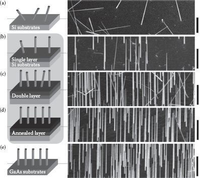
FIGURE 47.4 Schematic illustrations with SEM images of GaAs NWs grown on Si (111) substrates (a) without any buffer layer, (b) with a single GaAs buffer layer, (c) with a double GaAs buffer layer, and (d) with an annealed double GaAs buffer layer. (e) The morphology of GaAs NWs grown on GaAs (111)B substrates is shown in (e) for comparison; scale bars are 2 μm.
47.5 IMPROVEMENT OF CRYSTAL STRUCTURE OF III–V NANOWIRES
To obtain defect-free NWs, optimization of growth conditions in terms of growth temperature and a V/III ratio, together with a precursor flow rate was investigated in this study.
Figure 47.5 shows the illustrations of three different types of GaAs NWs grown for this study. Here, all NWs were grown on Si (111) substrates coated with annealed double GaAs buffer layers as discussed above (Figure 47.3b). The first set of GaAs NWs was grown at 450°C for 30 min with a V/III ratio of 46.3 as reference (NWN). The second set of GaAs NWs was grown via the two-temperature procedure (NWT) [14], where an initial nucleation temperature of 450°C was employed for a minute before growth was continued for 30 min at a reduced growth temperature of 375°C. The V/III ratio was maintained constant at 46.3. The last set of GaAs NWs was grown with a rapid growth rate (NWR) at 450°C for 6 min with the TMGa flow rate increased by a factor of 5 while maintaining the V/III ratio at 46.3. The growth time was reduced to have a comparable length as NWN.
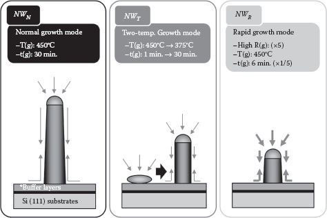
FIGURE 47.5 Illustration of the three types of GaAs NWs investigated: NWN grown by the normal procedure as a reference, NWT grown via a two-temperature procedure, and NWR grown via a rapid growth rate procedure. T(g): growth temperature, t(g): growth time, and R(g): growth rate.
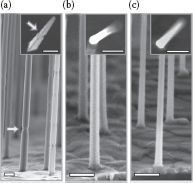
FIGURE 47.6 SEM images of (a) NWN, (b) NWT, and (c) NWR, respectively. The samples were tilted 10° from the normal surface. Arrows in the image (a) indicate surface grooves on the nanowires: all scale bars are 1 μm.
In Figure 47.6a, the reference GaAs NWs (NWN) are seen to be straight and vertical with serrated sidewalls (indicated by arrows) and substantial tapering, the latter two features being undesirable for device applications. These surface grooves and rotated body segments are related to the sidewall faceting behavior [11,14]. As shown in the inset image, the NW base appears to be a truncated triangular shape due to different {112}A and {112}B sidewall growth rates [12]. In contrast to the morphology of NWs grown at 450°C, GaAs NWs grown by the two-temperature procedure (NWT) in Figure 47.6b show much improved morphology with little tapering and smooth sidewalls. Also, the base of the NW appears to be almost hexagonal in shape (inset image). It should be noted that without the nucleation step at 450°C, all NWs grown (on GaAs substrate) at 375°C were kinked [14]. Similar to NWT, GaAs NWs with a high growth rate (NWR) (Figure 47.6c) also exhibit straight and vertical orientation with a smooth surface morphology. Significantly less tapering in comparison to NWN is noted, as has been reported for similar growths on GaAs (111)B substrates previously [17]. NWR also has a near hexagonal-shaped bottom as shown by the inset image.
High-magnification TEM images of these three NWs are shown in Figures 47.7a through 47.7c. All NWs have a ZB crystal structure that is consistent with previous reports [14,17]. NWN in Figure 47.7a, as discussed in Section 47.2.2, has some stacking faults and a serrated sidewall [11,13,18]. The HR-TEM image (inset) shows a thin twin defect across two ZB crystal segments (A–B–A type). This is in contrast with Figures 47.7b and 47.7c, where no such defects are present and the sidewalls are smooth. In the case of NWT, it is believed that the low growth temperature results in a twin-free ZB crystal structure due to the low supersaturation growth condition while the availability of high concentration of Ga and As adatoms for NWR is believed to reduce the Au–GaAs interfacial tension [17] and thus hinder the formation of twin planes [19].
47.6 OPTICAL PROPERTIES OF NANOWIRES FOR DEVICE APPLICATIONS
Photoluminescence (PL) is routinely used to characterize the optical properties of GaAs NWs. Bare GaAs NWs, however, emit only very weak PL, even at low temperatures [14,20,21], which is due to the high density of surface states that act as nonradiative recombination centers. These surface states not only quench GaAs NW PL but also adversely affect optoelectronic device performance. These surface states can be removed by cladding the GaAs NWs with a shell of a wider band-gap AlGaAs layer, creating a core–shell structure. Figure 47.8 shows a schematic image of core–shell (CS-) GaAs NWs with an AlGaAs/GaAs shell and SEM images for morphology of CS-NWN, CS-NWT, and CS-NWR, respectively. Here, the thin GaAs cap has a role to prevent the oxidation of the AlGaAs shell. The shell spatially separates the electronic states of the GaAs core from the surface and acts as a carrier reservoir for the inner core [22]. Thus, GaAs NWs capped by the AlGaAs shell have much a higher PL efficiency.
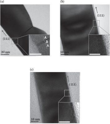
FIGURE 47.7 High-magnification TEM images and HR-TEM images (inset) of (a) NWN, (b) NWT, and (c) NWR, respectively. All scale bars in the inset images are 5 nm.
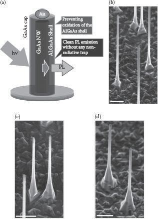
FIGURE 47.8 (a) Schematic image of core–shell (CS-) GaAs NWs with a AlGaAs/GaAs shell. (b)–(d) SEM images for morphology of CS-NWN, CS-NWT, and CS-NWR; all scale bars are 1 μm.
In Figure 47.9a, normalized micro-PL spectra from the three types of core–shell NW (CS-NW) samples are shown. Regular ripples in the PL spectra may be considered as artifacts arising from the interference filter used to remove the 1.65 eV laser line while broader structures come from the AlGaAs shell due to nonuniformities of the Al composition owing to changes in the Al incorporation rate with diameter [23,24]. All PL peaks are near 1.518 eV (±0.006 eV) and show a similarly strong intensity (albeit normalized here), which is attributed to free exciton recombination in bulk GaAs [20,25]. Figure 47.9b plots time-resolved (TR-) PL spectra at the free exciton recombination energy for each of the GaAs/AlGaAs CS-NWs. CS-NWN, grown with standard core-NWs (NWN), shows a short lifetime due to crystal defects inside the NW core (stacking faults and twin defects) while the two temperature growth, CS-NWT, exhibits the longest lifetime reflecting a high degree of crystalline quality [14,26]. Interestingly, CS-NWR grown with a rapid growth rate displayed a very short lifetime, which is also the resolution limit of our TR-PL measurement system, possibly due to the point defects as nonradiative recombination centers of gallium and arsenic-related defects such as vacancies, interstitials, and antisites.
For the integration of III–V device applications with Si-based electronics, well-aligned, straight morphology, and pure crystal structure without any structural defects, such as twin defects or stacking faults, are essential. In this chapter, it was demonstrated that straight, epitaxial GaAs NWs on Si substrates along the <111> direction can be achieved by first covering the Si surface with a thin GaAs buffer layer. A double-layer structure, consisting of an initial layer grown at a low temperature with a low V/III flow ratio and a subsequent layer grown at a high temperature with a high V/III flow ratio, was shown to produce a relatively flat surface with good crystalline quality; in situ annealing at high temperature further improved the surface morphology of the double buffer layers, and subsequently the yield of high-quality NWs. In addition, it was also demonstrated that defect-free GaAs NWs were obtained by using specific growth techniques, such as the two-temperature growth and rapid growth rate. The rapid growth rate method resulted in the highest yield of straight and vertical NWs while the two-temperature growth method resulted in the longest exciton lifetime and least tapering, which are desirable for optoelectronic device applications. These results show promise for the future integration of III–V NW optoelectronic devices with Si-based microelectronic devices.
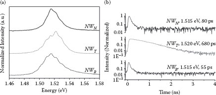
FIGURE 47.9 Normalized (a) micro- and (b) time-resolved (TR)-photoluminescence (PL) emission peaks of CS-NWN, CS-NWT, and CS-NWR.
The Australian Research Council is gratefully acknowledged for the financial support. This work was performed in part using the ACT Node of the Australian National Fabrication Facility (ANFF).
1. N. Dasgupta and A. Dasgupta, Semiconductor Devices—Modelling and Technology, Prentice Hall of India, New Delhi, 2004, pp. 56–57.
2. R. Chau, S. Datta, M. Doczy, B. Doyle, B. Jin, J. Kavalieros, A. Majumdar, M. Metz, and M. Radosavljevic, Benchmarking nanotechnology for high-performance and low-power logic transistor applications, IEEE Trans. Nanotechnol., 2005, 4, 153–158.
3. H. S. P. Wong, Beyond the conventional transistor, J. IBM Res. Dev., 2002, 46, 133–168.
4. V. A. Sverdlov, T. J. Walls, and K. K. Likharev, Nanoscale silicon MOSFETs: A theoretical study, IEEE Trans. Electron Devices, 2003, 50, 1926–1933.
5. A. A. Bergh and P. J. Dean, Light-Emitting Diodes, Clarendon, Oxford, 1976.
6. C. Jeong, S. W. Lee, J. M. Seo, and J. M. Myoung, The effect of stacking fault formation on optical properties in vertically aligned ZnO nanowires, Nanotechnology, 2007, 18, 305701.
7. T. M. Chang and E. A. Carter, Structures and growth mechanisms for heteroepitaxial fcc (111) thin metal films, Phys. Chem., 1995, 99, 7637–7648.
8. T. Mårtensson, C. P. T. Svensson, B. A. Wacaser, M. W. Larsson, W. Seifert, K. Deppert, A. Gustafsson, L. R. Wallenberg, and L. Samuelson, Epitaxial III-V nanowires on silicon, Nano Lett., 2004, 4, 1987–1999.
9. X.Y. Bao, C. Soci, D. Susac, J. Bratvold, D. P. R. Aplin, W. Wei, C.Y. Chen, S. A. Dayeh, K. L. Kavanagh, and D. Wang, Heteroepitaxial growth of vertical GaAs nanowires on Si (111) substrates by metal-organic chemical vapour deposition, Nano Lett., 2008, 8, 3755–3760.
10. L. Roest, M. A. Verheijen, O. Wunnicke, S. Serafin, H. Wondergem, and E. P. A. M. Bakkers, Positioncontrolled epitaxial III–V nanowires on silicon, Nanotechnology, 2006, 17, S271–S275.
11. J. Zou, M. Paladugu, H. Wang, G. J. Auchterlonie, Y. N. Guo, Y. Kim, Q. Gao, H. J. Joyce, H. H. Tan, and C. Jagadish, Growth mechanism of truncated triangular III-V nanowires, Small, 2007, 3, 389–393.
12. J. Johansson, L. S. Karlsson, C. P. T. Svensson, T. Mårtensson, B. A. Wacaser, K. Deppert, L. Samuelson, and W. Seifert, Structural properties of <111> B -oriented III–V nanowires, Nat. Mater., 2006, 5, 574–580.
13. J. Bauer, V. Gottschalch, H. Paetzelt, G. Wagner, B. Fuhrmann, and H. S. Leipner, MOVPE growth and real structure of vertical-aligned GaAs nanowires, J. Cryst. Growth, 2007, 298, 625–630.
14. H. J. Joyce, Q. Gao, H. H. Tan, C. Jagadish, Y. Kim, Z. Zhang, Y. N. Guo, and J. Zou, Twin-free uniform epitaxial GaAs nanowires grown by a two-temperature process, Nano Lett., 2007, 7, 921–926.
15. K. Kitahara, M. Ozeki, and K. Nakajima, Reflection high-energy electron diffraction of heteroepitaxy in chemical vapour deposition reactor: Atomic-layer epitaxy of GaAs, AlAs and GaP on Si, Jpn. J. Appl. Phys., 1993, 32, 1051–1055.
16. Y. B. Bolkhovityanov and O. P. Pchelyakov, GaAs epitaxy on Si substrates: Modern status of research and engineering, Physics-Uspekhi, 2008, 51, 431–456.
17. H. J. Joyce, Q. Gao, H. H. Tan, C. Jagadish, Y. Kim, M. A. Fickenscher, S. Perera et al., Unexpected benefits of rapid growth rate for III − V nanowires, Nano Lett., 2009, 9, 695–701.
18. K. A. Dick, P. Caroff, J. Bolinsson, M. E. Messing, J. Johansson, K. Deppert, L. R. Wallenberg, and L. Samuelson, Control of III–V nanowire crystal structure by growth parameter tuning, Semicond. Sci. Technol., 2010, 25, 204009.
19. Q. Li, X. Gong, C. Wang, J. Wang, K. Ip, and S. Hark, Size-dependent periodically twinned ZnSe nanowires, Adv. Mater., 2004, 16, 1436–1440.
20. L. V. Titova, T. B. Hoang, H. E. Jackson, L. M. Smith, J. M. Yarrison-Rice, Y. Kim, H. J. Joyce, H. H. Tan, and C. Jagadish, Temperature dependence of photoluminescence from single core-shell GaAs-AlGaAs nanowires, Appl. Phys. Lett., 2006, 89, 173126.
21. H. J. Joyce, Q. Gao, H. H. Tan, C. Jagadish, Y. Kim, J. Zou, L. M. Smith et al., III–V semiconductor nanowires for optoelectronic device applications,. Prog. Quantum Electron., 2011, 35, 23–75.
22. F. Jabeen, S. Rubini, V. Grillo, L. Felisari, and F. Martelli, Room temperature luminescent InGaAs/GaAs core–shell nanowires, Appl. Phys. Lett., 2008, 93, 083117.
23. J. Noborisaka, J. Motohisa, S. Hara, and T. Fukui, Fabrication and characterization of freestanding GaAs/AlGaAs core-shell nanowires and AlGaAs nanotubes by using selective-area metalorganic vapour phase epitaxy, Appl. Phys. Lett., 2005, 87, 093109.
24. F. Bailon-Sominatic, J. J. Ibanez, R. B. Jaculbia, R. A. Loberternos, M. J. Defensor, A. A. Salvador, and A. S. Sominac, Low temperature photoluminescence and Raman phonon modes of Au-catalyzed MBEgrown GaAs-AlGaAs core-shell nanowires grown on a pre-patterned Si (111) substrate, J. Cryst. Growth, 2011, 314, 268–273.
25. V. Swaminathan, D. L. V. Haren, J. L. Zilko, P. Y. Lu, and N. E. Schumaker, Characterization of GaAs films grown by metalorganic chemical vapour deposition, J. Appl. Phys., 1985, 57, 5349–5353.
26. P. Parkinson, H. J. Joyce, Q. Gao, H. H. Tan, X. Zhang, J. Zou, C. Jagadish, L. M. Herz, and M. B. Johnston, Carrier lifetime and mobility enhancement in nearly defect-free core-shell nanowires measured using time-resolved terahertz spectroscopy, Nano Lett., 2009, 9, 3349–3353.