
Synthesis and Characterization of n- and p-Doped Tin Oxide Nanowires for Gas Sensing Applications |
CONTENTS
48.2.2 Material Characterizations
48.2.4 Cl2 Sensor Fabrication and Characterization
48.3.1 Sensor Application of n-Doped NWs: Chlorine Detection
1D nanostructure materials have attracted great attention in recent years1,2,3 as they provide interesting possibilities for resistance-less transport due to quantum effects. Another remarkable property of such 1D semiconductor materials is their sensitivity to ambient conditions such as humidity, oxygen level, and so on. Their resistance can be modulated by adsorbed gases capable of electron/hole injection/withdrawal from conduction and valence bands. Such an electron transfer creates a carrier depletion layer near the solid–air interface increasing the device impedance. This increase/decrease in resistance provides a convenient response with respect to analyte concentration. Furthermore, the sensor devices can be made more specific for a given type of gas through the use of dopants that selectively interact with the analyte gas. Additionally, doping can further amplify the device sensitivity and its dynamic range by providing an increase in the carrier concentration.
The most common method for the synthesis of 1D nanowires (NWs)/nanotubes (NTs) is based on the vapor–liquid–solid (VLS) mechanism that can be carried out in a chemical vapor deposition (CVD) reactor. VLS is considered to be one of the best methods for producing single-crystal NWs and NTs in relatively large quantities.4,5 An adaptation of the VLS method involving solution–liquid–solid phases is developed by Buhro et al.6 A similar solvothermal method uses solvents under very specific conditions of pressure and temperature to increase the solubility of solids and speeds up reactions7 that lead to the formation of NWs. Solution-state methods involving templating by a combination of surfactants that preferentially cap the sidewalls of growing NWs have also been developed for the synthesis of metallic NWs of gold, silver, and so on.8,9
This chapter focuses on solution-state syntheses of doped SnO2 NWs. A key benefit of tin oxide over other contemporary semiconductors such as silicon or gallium arsenide and even carbon nanotubes (CNTs) is that it is a chemically stable material that is corrosion resistant. Thus, this wide bandgap semiconductor (3.56 eV) finds wide-ranging applications in nanoelectronics as a transparent conductor,10,11,12,13 in chemistry as heterogeneous catalysts,14,15,16,17,18,19 and also as a solid-state gas sensor.20,21,22,23,24,25 In a series of papers, we have illustrated the synthesis,26 characterization,26 and applications22,27 of nanoparticles (NPs) of SnO2. Using compressed powders of n-doped and p-doped SnO2 NPs, we have been able to fabricate homo-junction diode sensors capable of detecting the 100 ppb level of a toxic oxidizing gas, chlorine. One key limitation of these sensors arises from poor electron transport across the NP powders. This is a result of the interparticle depletion barrier and the effects of coulomb blockade at each physical contact. Practically, this limits the dynamic range of devices confining them to low concentration (below 20 ppm) of the analyte. A simple method to minimize these interparticle electron/hole hops is through the replacement of NPs with aligned NWs. The resistance for transport along the single-crystal nanowire is lower due to the favorable quantum effects in 1D systems.28 Studies of electron transport through CNTs and SiNWs indicate extraordinarily high mobility in these 1D quantum fluids.29,30
Our goal here is to present synthetic methods for synthesizing doped NWs for tin oxide and illustrate their application in gas sensing. Current methods so far for the synthesis of 1D nanostructures of undoped SnO2 include laser ablation,31,32 molten salt,33,34 solvothermal and hydrothermal methods,35,36 thermal evaporation,37,38 carbothermal reduction,39,40 and rapid oxidation.41 Herein, we describe the synthesis of doped SnO2 NWs adopting and modifying the strategy of Yang and Lee.33 It has enabled us to synthesize n-type, antimony-doped SnO2 NWs. We introduce the first synthesis of a p-doped SnO2 1D nanostructure using lithium ion as a dopant. The latter is developed based on our current understanding of p-doped SnO2 NPs.26,42.43 We also present a comparison of the structural and optical properties of SnO2 NPs and SnO2 NWs. Both n- and p-type NWs display a characteristic red shift in their photoluminescence (PL) spectra. Surface plasmons observed in these systems imply high carrier concentrations. These corrosion-resistant materials are useful in fabricating ultrasensitive gas detectors and transparent electronics, and we demonstrate the application to toxic gas Cl2.
The following chemicals were used without further purification: SnCl4⋅5H2O (>98%, Fischer Scientific), 1,10-phenanthroline monohydrate (ACS reagent, puriss. p.a., ≥99.5%, Sigma Aldrich), NaBH4 (98%, Sigma Aldrich), LiCl, KCl, and NaCl (>95%, Fischer Scientific).
48.2.2 MATERIAL CHARACTERIZATIONS
SEM data were collected on an FEI Sirion FEG SEM operating at 5 KV with a working distance of 5 mm. TEM data were collected using Holey carbon TEM grids on a FEI Tecnai F-20 microscope operating at 200 kV. The optical PL of the doped and undoped SnO2 NWs was characterized on a Shimadzu spectrofluorophotometer RF-5301PC, using a xenon light source and a 3 nm bandwidth. As-prepared samples including NPs and NWs were dispersed in water for the PL measurements. Fourier transform infrared (FTIR) spectra were acquired on a Perkin-Elmer RXI instrument. For infrared as well as UV–visible–NIR (Shimadzu UV 3600) spectroscopic investigations, samples consisted of solid powders sandwiched between quartz plates. This protocol is different from the commonly used, solvent-dispersed studies of these materials.
n-Doped tin oxide NWs: The precursor Sn NPs were synthesized by reducing a thoroughly mixed solution of 50 mL of 0.05 M SnCl4⋅5H2O and 0.5 g of 1,10-phenanthroline with 100 mL of 0.1 M NaBH4 aqueous solution. The reducing solution was introduced dropwise to synthesize phenanthroline-capped Sn NPs.44 NPs were separated from the reaction mixture by centrifuging (10,000 rpm for 15 min) after 2 h of reaction time. The precipitate was dried at 50°C for 2 h on a hot plate. 0.2 g of 1,10-phenanthroline-capped Sn NPs powder was mixed with a mixture of 0.4 g of NaCl and 0.6 g of KCl, grounded into a fine powder, and heated at 750°C for 2 h in a furnace. The molten mixture was then slowly cooled to room temperature. The solidified product was washed several times with water, to remove KCl and NaCl. Salt removal was tested with 0.05 mM AgNO3 solution for any residual Cl− anion. The wet powder was dried in an oven at 100°C overnight to remove water. For n-doping, varying amounts of antimony chloride (1–5% at.wt. in relation to Sn) were added to the initial solution of SnCl4⋅5H2O and 1,10-phenanthroline. The rest of the synthetic procedure was identical to the synthesis of undoped NWs as described above. Note that the actual amount of dopant inserted in NPs could be different from the concentration of dopant used during synthesis (see below).
A slightly modified synthetic method was developed to produce much higher quantities of undoped SnO2 and n-doped SnO2 NWs. 5 g of SnCl4⋅5H2O in was dissolved in 150 mL (antimony chloride was added for the synthesis of n-doped nanowires) water. The solution was stirred for 15 min before the continuous dropwise addition of 50 mL of 4% NaBH4 (aqueous) solution. The mixture turned black, indicating the formation of oxide-coated Sn NPs. The precipitate was collected by filtering and was left to dry in air overnight. 2 g of the above precursor was mixed with 0.2 g of 1,10-phenanthroline, 4 g of NaCl, and 6 g of KCl, ground into a fine powder, and kept at 750°C for 2 h.
p-Doped tin oxide NWs: For p-doping, LiCl replaced antimony chloride as a dopant. The amounts of lithium chloride added to the initial reaction mixture ranged from 1 to 5 wt%. The precursor Sn NPs coated with a thin layer of tin oxide were synthesized in a similar manner to that in which LiCl was replaced as the doping agent. 0.2 g of the above as-synthesized precursors was mixed with 0.2 g of 1,10-phenanthroline, 0.31 g of LiCl, and 0.6 g of KCl, ground into a fine powder, and kept at 480°C (which is near the eutectic temperature and composition for the LiCl/KCl mixture) for 2 h. The choice of this temperature is critical, as at a higher temperature Li2SnO3 begins to form and phase separate from the SnO2 lattice. Furthermore, the presence of LiCl in liquid form enables a higher degree of p-doping in this synthetic method. The molten mixture was then slowly cooled to room temperature with a cooling rate of 4°C/min. The product was collected and purified as in the case of undoped NWs.
48.2.4 CL2 SENSOR FABRICATION AND CHARACTERIZATION
To fabricate the sensor, a simple powder compression technique was employed. For the chlorine sensor, 2 g of Sb-doped SnO2 was mixed with 0.5 mL of 2% ethyl silicate in acidified ethanol. The paste was compressed using a pressure of 5463 kg/cm2 to yield a 13 mm (diameter) pellet with a thickness of 800 μm. The pellet was heated at 450°C for 30 min. It was then mounted onto a glass substrate and copper contacts attached using conductive silver epoxy.
The sensor performance was tested in a home-built test chamber at room temperature. The resistance of the sensor material was monitored by a Fluke 8840A multimeter, which was interfaced to a National Instrument’s GPIB-PCII interface on a personal computer. During the measurements, there was a continuous flow of diluted test gas (10 L/min) into the test chamber (volume 1.2 L) (illustrated below). The sensor response time was measured by analyzing resistance versus time data. To refresh the sensor, a flow of fresh air was maintained in the chamber and the sensor temperature was adjusted. The sample temperature could be maintained between 25°C and 120°C by varying the resistive heater voltage (0–5 V). A Cr–Al thermocouple was placed on the surface of the sensor to measure the sensor operating temperature. The output of the thermocouple was fed to a temperature indicator Mastech (MAS-345) multimeter. A schematic view of the sensor testing system is shown in Figure 48.1.
The sensor response was defined as (RChlorine − RAir)/RAir air. Typically, the measurements were repeated three times and the sensor measurements were reproducible over a period of a week at Cl2 concentrations (<1 ppm (μg of Cl2 per g of carrier gas)), while a steady drift in resistance was observed at high chlorine concentrations, perhaps due to the formation of AgCl at the electrode contact points.
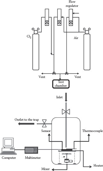
FIGURE 48.1 Outline of the dynamic sensor testing system.
The bulk-scale synthesized powders of NWs exhibit distinct colors (Figure 48.2). The undoped NWs are pale yellow; p-doped NWs are deeper yellow; while the n-doped NWs are dark blue. This may simply reflect the higher carrier concentration in n-doped systems.
The morphology of the as-prepared undoped and Sb-doped SnO2 NWs was characterized by SEM; see Figure 48.3. The majority of the undoped NWs showed an average NW diameter ranging from 20 to 50 nm and lengths up to a few microns. This NW structure was mixed with a small portion of whisker-like nanorod structure. In n-doped NWs, the size distribution was much broader due to the incorporation and morphological effects of dopant atoms (see below). Also, note that the smaller-diameter NWs tended to fuse with one another. Since such structures are rarely observed in the nucleation and growth of NWs mediated by the VLS mechanism, the mechanism of growth of these NWs is likely to be governed by the surface energy of NW walls as controlled by the capping agent phenanthroline. TEM and the high-resolution TEM of n-doped NWs, shown in Figure 48.3 along with the electron diffraction as inset, indicated a single crystalline nature of the synthesized NWs. The crystal structure of these 20 nm diameter NWs was a characteristic cassiterite type (details are not shown here), which is commonly observed upon calcination at 500°C in SnO2 NPs synthesized by the sol–gel method.26 Also, it can be seen that the nanowire growth mechanism is neither VLS (no spherical catalyst droplet on the tip) nor solution–liquid–solid (SLS). The NWs showed a very straight and smooth surface morphology suggesting a 1D Ostwald ripening mechanism34 in which NPs deposit onto, dissolve into each other, and extrude to form a 1D nanostructure.
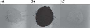
FIGURE 48.2 Bulk-scale synthesized (a) undoped, (b) n-doped, and (c) p-doped SnO2 nanowires.
Room-temperature PL spectra of undoped SnO2 NPs and NWs appear in Figure 48.4. The excitation wavelength used in this study was 310 nm corresponding to energy greater than the bulk bandgap energy for SnO2. Two different PL characteristics were observed for NPs and NWs. Both nanostructures gave a strong UV emission at 360 nm, corresponding to the bandgap of SnO2 (3.56 eV), which partially overlapped with the Raman scattering of water. The latter peak appears at a constant frequency offset from the excitation wavelength.
Bulk SnO2 is an indirect bandgap semiconductor, so it is not expected to have a strong PL corresponding to its bandgap energy, as it would violate the principle of momentum conservation. Observation of PL in these nanogeometries (i.e., in both NPs and NWs) implies a PL characteristic of a direct bandgap-type semiconductor. Similar effects are well known in silicon NPs; porous silicon and silicon NWs45 are not still well understood. Interestingly, the NWs have an additional broad emission peak near 460 nm (2.7 eV). A precise understanding of this PL peak does not exist currently, although explanations in terms of defects, including vacancies of oxygen, dopant segregation, and lattice disorders inside the lattice of SnO234,46,47,48 or near surface, can be advanced.
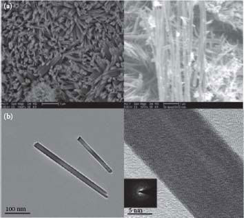
FIGURE 48.3 (a) SEM images of undoped (left) and Sb-doped NWs (right). (b) TEM of n-doped SnO2 NWs with low and high magnifications. (H.A. Tran and S.B. Rananavare, Synthesis and characterization of N- and P-doped tin oxide nanowires. 2011 11th IEEE Conference on Nanotechnology (IEEE-NANO), Aug. 15–18, 144–149, © (2011) IEEE. With permission.)
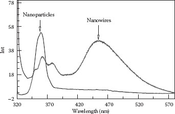
FIGURE 48.4 PL of undoped NWs and NPs (excitation wavelength 310 nm). (H.A. Tran and S.B. Rananavare, Synthesis and characterization of N- and P-doped tin oxide nanowires. 2011 11th IEEE Conference on Nanotechnology (IEEE-NANO), Aug. 15–18, 144–149, © (2011) IEEE. With permission.)
The presence of a dopant, especially in high concentrations, can lead to an impurity band near the conduction (in the case of an n-type dopant) or valence (in the case of p-type dopant) bands. The resulting bandgap narrowing could result in a red shift in the PL. As shown in Figure 48.5, under the same excitation wavelength of 280 nm, both undoped and n-doped SnO2 NWs gave two UV emission peaks, one at 310 nm, which is due to the solvent Raman scattering, and the other broad peak at 360 nm wavelength for n- and p-doped nanowires, but for undoped nanowires, it is at 340 nm. For the latter peak, the observed red shift of 20 nm is consistent with a dopant-induced bandgap narrowing concept.
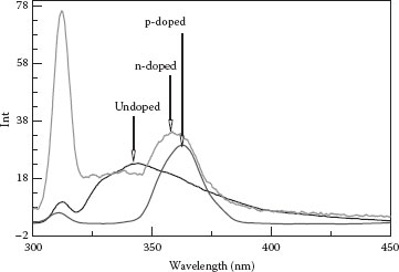
FIGURE 48.5 PL of undoped, 5% n-doped, and 5% p-doped SnO2 NWs. (H.A. Tran and S.B. Rananavare, Synthesis and characterization of N- and P-doped tin oxide nanowires. 2011 11th IEEE Conference on Nanotechnology (IEEE-NANO), Aug. 15–18, 144–149, © (2011) IEEE. With permission.)
At this time, we do not have an adequate explanation for the disappearance of the 450 nm peak observed in undoped NWs when excited with a 310 nm wavelength (Figure 48.4). The currently accepted interpretation of the 450 nm peak, ascribed to oxygen vacancies, cannot explain the disappearance of this peak when excited by a 280 nm wavelength.
Figure 48.6 shows the I–V characteristics of n-type NWs as a function of dopant concentration. To carry out these measurements, powders of NWs were compressed into the pellets22 and silver epoxy contacts were used. Good ohmic contacts were observed due to degenerate doping. As the impurity concentration is increased, the conductivity significantly increases and achieves its maximum value at 5% dopant concentration. However, at higher dopant concentration, a decrease in the conductivity was observed. Nanoscopic phase separation of the Sb2O5 (insulating amorphous) layer from SnO2 that wraps around NWs can explain this anomalous conductivity. This phenomenon can also decrease the carrier mobility.
Figure 48.7 presents SEM images of p-doped NWs. Broad size distributions for length and diameter were observed. The length of wires varied from 200 nm up to a few μm while the diameter of a single wire ranged from 50 nm to hundreds of nanometers. Like n-doped NWs, whisker-like nanorods with smaller diameters and shorter lengths were also observed along with the tendency of NWs to fuse. Thus, preformed NPs transformed into NWs through recrystallization from alkali halide salts exhibited similar characteristics regardless of the nature (n or p type) of the dopant. The morphology of the NW nanostructure was influenced by a variety of other factors, such as precursors, growth temperature, and the moisture content of the ground mixture before recrystallization. The presynthesized powder, when dried to get rid of the moisture, gave a better yield of wires and more uniform dimensional distributions. Also, the NWs formed at temperatures higher than 450°C gave longer wires (>1 μm in length) with more uniform length distribution as shown in Figure 48.7.
The effect of different synthetic conditions is shown in Table 48.1. Replacing coated Sn NP precursors by SnO NPs49 did not produce NWs at 450°C. However, recrystallization at 750°C did produce NWs with low yield.
Single crystalline SnO-coated Sn NP precursors and NWs were observed in TEM (Figure 48.8a). NPs showed a spherical shape with a mean diameter around 10 nm, as well as a tendency to agglomerate due to the absence of an interfacial capping agent.
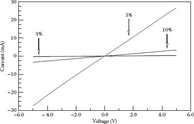
FIGURE 48.6 I–V curves of n-doped NWs at different dopant concentrations.
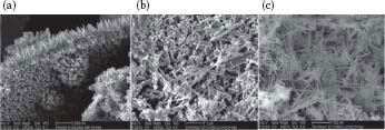
FIGURE 48.7 SEM image of p-doped SnO2 NWs synthesized at (a) 480°C, (b) 600°C, and (c) 700°C.
TABLE 48.1
Characteristics of p-Doped SnO2 Nanowires (NW) Synthesized from Sn Nanoparticles under Varying Synthetic Conditions
Temperature (°C) |
In Stagnant Air |
N2 Flow (120 sccm) |
Air Flow (120 sccm) |
Phenanthroline |
480 |
No NWs |
200–500 nm size (length) NWs |
No NWs, but NPs observed |
200 nm–1 μm size NWs |
600 or 700 |
2–5 μm size NWs and mixed with NPs |
Not tested |
Not tested |
2–5 μm long NWs |
The agglomeration of NPs was perhaps responsible for the observed fused NWs during the growth process. HR-TEM images of p-doped SnO2 NWs shown in Figure 48.8b indicated their single crystalline nature, which was further confirmed by electron diffraction shown in the inset of Figure 48.8b. The TEM data showed that an interplanar spacing is about 0.34 nm, which corresponds to the (110) plane of the cassiterite crystal structure of SnO2.
Tin oxide doping was also investigated through studies of surface plasmons as it provides a convenient means of determining the carrier concentration by contact-free measurement. Specifically, the surface plasmon resonance frequency is given by
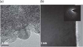
FIGURE 48.8 (a) TEM of SnO2−x-coated Sn NP precursors and (b) TEM of p-doped SnO2 NWs with inset showing selective area electron diffraction. (H.A. Tran and S.B. Rananavare, Synthesis and characterization of N- and P-doped tin oxide nanowires. 2011 11th IEEE Conference on Nanotechnology (IEEE-NANO), Aug. 15–18, 144–149, © (2011) IEEE. With permission.)
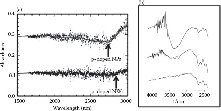
FIGURE 48.9 (a) Optical absorption spectra for p-doped NP and NWs. The surface plasmon peaks are just beyond the range of the instrument. Smooth lines are drawn to guide the eye. (b) FTIR spectra of p-doped NPs (top), NWs (middle), and quartz substrate (bottom). Note that the y-axis scale is transmittance and the spectra are shifted vertically for better display. The surface plasmon wavelength for NPs is about 3400 nm and the corresponding carrier density is 1.6 × 1020 cm−3. The carrier density for the p-doped NWs is similar. (H.A. Tran and S.B. Rananavare, Synthesis and characterization of N- and P-doped tin oxide nanowires. 2011 11th IEEE Conference on Nanotechnology (IEEE-NANO), Aug. 15–18, 144–149, © (2011) IEEE. With permission.)
Where ωSP is the observed surface plasmon resonance peak frequency and γ is its width; εm and ε0 are the dielectric constant and dielectric permittivity of the space, respectively; and mh and Nh are the hole mass and concentration in the SnO2 semiconductor, respectively; and e is the electronic charge. For Sb-doped tin oxide NPs, the surface plasmons in the near-IR to mid-IR range were observed and carrier densities in the range of 1020–1022 cm−3 were reported50 for 5–20% dopant concentration.* Our studies of n-doped NPs and NWs gave surface plasmon peaks near 2300 nm (not shown) corresponding to the carrier density of 1 × 1022 cm−3.
UV–visible–NIR studies of p-doped NPs and NWs, shown in Figure 48.9, suggested a shift in the surface plasmon resonance peak to the mid-IR region reflecting a significant reduction in the carrier density for p-type NWs and NPs. Note that even an undoped SnO2 tends to be an n-type semiconductor due to the nonstoichiometric nature of the oxide, that is, it is SnO2−x and not SnO2, where x is small but positive. The loss of oxygen deposits excess electrons in the conduction band and positively charged immobile oxygen vacancies in the crystalline lattice. Thus, to realize a p-type semiconductor, the excess electrons have to be first neutralized, that is, the Fermi level has to be pushed toward the valence band requiring significantly higher p-type dopant concentration26,42 to insert the equivalent hole carrier density. To verify if the surface plasmon peak indeed appears in the mid-IR region, we collected IR spectra from the powders of NP and NWs. The data, shown in Figure 48.9b, exhibited a strong peak near the 3400 nm region, that is, a clear continuation of the incipient peaks seen in the NIR spectra as seen in UV–visible spectra shown in Figure 48.9a. The corresponding carrier concentration was 1.6 × 1021 cm−3 for p-doped NPs.
Interestingly, the plasmon peak position for the p-doped NWs barely shifted from its location in p-type NPs, yet the width of the peak was clearly broader, implying a shorter collisional lifetime of the carriers. This could arise from the relatively high surface area to volume ratios for NWs than NPs. The failure to shift the peak to lower wavelengths, that is, lower concentration of inserted p-type dopants (even when synthesized in LiCl solvent), could imply a radial concentration gradient of the dopant or even the formation on the NW outer shell. Further NMR studies are currently underway to explore the location of the inserted Li in the NWs.
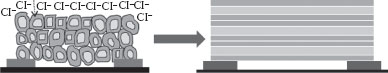
FIGURE 48.10 Schematic illustration of depletion regions in NPs (left) and NWs (right) upon exposure to oxidizing gas such as chlorine in the SnO2-based resistive sensor.
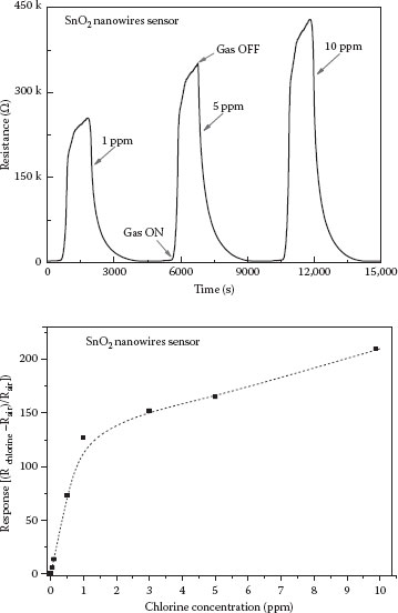
FIGURE 48.11 Time-dependent resistance change as a function of chlorine concentration and overall response concentration curve.
48.3.1 SENSOR APPLICATION OF n-DOPED NWS: CHLORINE DETECTION
The success of using n-doped SnO2 NPs as a smart sensor based on noncorrodible SnO2 NPs to selectively detect chlorine at room temperature22 was the motivation for the current synthesis of n-doped nanowires. The basic mechanism of the increase in the resistance of the sensor is due to the creation of the depletion layer and an associated barrier for electron tunneling. Increasing the concentration of chlorine in the gas phase results in a proportionate increase in the chloride ion concentration at the gas–solid interface, which in turn increases the depletion region and hence the resistance of the sensor. This is shown schematically in Figure 48.10.
Replacing n-doped NPs with n-doped nanowires should lead to a faster response by reducing the number of interparticle electron hops between the sensing electrodes (Figure 48.10, right).
The data in Figure 48.11 show a monotonic response with Cl2 concentration. It should be noted that the switching speeds near room temperature are about 4–5 min. These n-doped NW-based sensors are capable of pushing the chlorine detection limit to the ppb level. By analogy, an increase in impedance is expected for reducing gases with p-type SnO2 nanowires. Currently, our ongoing studies of H2 gas detection have shown a relatively poor sensitivity for its detection using p-type nanowires/nanoparticles. We ascribe these effects to the mid-bandgap location of the H2 redox level.
The sensitivity of these devices can be improved by using palladium (Pd) nanoparticles. Pd can absorb and presumably form hydrides in the presence of hydrogen gas. Interestingly, Pd nanoparticle composites of n-type nanowires were sensitive to H2 gas. The results of these extensive studies will be reported elsewhere.
The first synthesis of single crystalline n-doped and p-doped SnO2 NWs is reported. These structures exhibit two strong emission bands in the fluorescence spectra and display surface plasmon peaks in the near- to mid-IR regions, implying a high carrier concentration. The availability of both n- and p-type NWs opens up new opportunities for crafting transparent nanoelectronic devices, sensors, and so on. Preliminary studies of the sensor properties of n-type NW-based devices have yielded ppb-level sensitivity for chlorine gas detection.
We are indebted to Professors Carl C. Wamser and Andrea M. Goforth for allowing access to UV–visible–NIR and fluorescence spectrometers, respectively. Partial financial support from Intel Corporation NIH and ONAMI is gratefully acknowledged.
1. A. P. Alivisatos, Science 1996, 271, 933–937.
2. C. Dekker, Physics Today 1999, 52, 22–28.
3. J. Hu, T. W. Odom, and C. M. Lieber, ChemInform 1999, 32, 435–445.
4. R. S. Wagner and W. C. Ellis, Applied Physics Letters 1964, 4, 89–90.
5. X. Duan and C. M. Lieber, Advanced Materials 2000, 12, 298–302.
6. T. J. Trentler, K. M. Hickman, S. C. Goel, A. M. Viano, P. C. Gibbons and W. E. Buhro, Science 1995, 270, 1791–1794.
7. J. R. Heath and F. K. LeGoues, Chemical Physics Letters 1993, 208, 263–268.
8. F. Kim, K. Sohn, J. Wu and J. Huang, Journal of the American Chemical Society 2008, 130, 14442–14443.
9. G. Yan, L. Wang and L. Zhang, Reviews on Advanced Materials Science 2010, 24, 10–25.
10. I. Hamberg and C. G. Granqvist, Journal of Applied Physics 1986, 60, R123–R159.
11. J. F. Wager, Science 2003, 300, 1245–1246.
12. R. L. Hoffman, B. J. Norris and J. F. Wager, Applied Physics Letters 2003, 82, 733–735.
13. R. E. Presley and et al., Journal of Physics D: Applied Physics 2004, 37, 2810.
14. G. E. Batley, A. Ekstrom and D. A. Johnson, Journal of Catalysis 1974, 34, 368–375.
15. G. Croft and M. J. Fuller, Nature 1977, 269, 585–586.
16. G. C. Bond, L. R. Molloy and M. J. Fuller, Journal of the Chemical Society, Chemical Communications 1975, 19, 796–797.
17. P. G. Harrison, C. Bailey and W. Azelee, Journal of Catalysis 1999, 186, 147–159.
18. F. Solymosi and J. Kiss, Journal of Catalysis 1978, 54, 42–51.
19. T. Matsui, T. Okanishi, K. Fujiwara, K. Tsutsui, R. Kikuchi, T. Takeguchi and K. Eguchi Science and Technology of Advanced Materials 2006, 7, 524–530.
20. C. Cané, I. Gràcia, A. Götz, L. Fonseca, E. Lora-Tamayo, M. C. Horrillo, I. Sayago, J. I. Robla, J. Rodrigo and J. Gutiérrez, Sensors and Actuators B: Chemical 2000, 65, 244–246.
21. F. Allegretti, N. Buttá, L. Cinquegrani and S. Pizzini, Sensors and Actuators B: Chemical 1993, 10, 191–195.
22. A. Chaparadza and S. B. Rananavare, Nanotechnology 2008, 19, 245501.
23. N. Buttà, L. Cinquegrani, E. Mugno, A. Tagliente and S. Pizzini, Sensors and Actuators B: Chemical 1992, 6, 253–256.
24. J. Tamaki, T. Maekawa, N. Miura and N. Yamazoe, Sensors and Actuators B: Chemical 1992, 9, 197–203.
25. J. M. Wu, Nanotechnology 2010, 21, 235501.
26. A. Chaparadza, S. B. Rananavare and V. Shutthanandan, Materials Chemistry and Physics 2007, 102,176–180.
27. J. C. Chan, N. A. Hannah, S. B. Rananavare, L. Yeager, L. Dinescu, A. Saraswat, P. Iyer and J. P. Coleman, The Japan Society of Applied Physics 2006 45, L1300–L1303.
28. F. D. M. Haldane, Journal of Physics C: Solid State Physics 1981, 14, 2585.
29. T. Darkop, S. A. Getty, E. Cobas and M. S. Fuhrer, Nano Letters 2003, 4, 35–39.
30. O. Gunawan, L. Sekaric, A. Majumdar, M. Rooks, J. Appenzeller, J. W. Sleight, S. Guha and W. Haensch, Nano Letters 2008, 8, 1566–1571.
31. J. Q. Hu, Y. Bando, Q. L. Liu and D. Golberg, Advanced Functional Materials 2003, 13, 493–496.
32. Z. Liu, D. Zhang, S. Han, C. Li, T. Tang, W. Jin, X. Liu, B. Lei and C. Zhou, Advanced Materials 2003, 15, 1754–1757.
33. Y. Wang and J. Y. Lee, The Journal of Physical Chemistry B 2004, 108, 17832–17837.
34. W. Wang, J. Niu and L. Ao, Journal of Crystal Growth 2008, 310, 351–355.
35. C. Yu, J. C. Yu, F. Wang, H. Wen and Y. Tang Crystal Engineering Communication 2010, 12, 341–343.
36. Z. Guifu et al., Nanotechnology 2006, 17, S313.
37. Z. W. Pan, Z. R. Dai and Z. L. Wang, Science 2001, 291, 1947–1949.
38. H. Kim, J. Lee and C. Lee, Journal of Materials Science: Materials in Electronics 2009, 20, 99–104.
39. J. X. Wang, D. F. Liu, X. Q. Yan, H. J. Yuan, L. J. Ci, Z. P. Zhou, Y. Gao et al., Solid State Communications 2004, 130, 89–94.
40. P. Nguyen, H. T. Ng, J. Kong, A. M. Cassell, R. Quinn, J. Li, J. Han, M. McNeil and M. Meyyappan, Nano Letters 2003, 3, 925–928.
41. X. L. Ma, Y. Li and Y. L. Zhu, Chemical Physics Letters 2003, 376, 794–798.
42. A. Chaparadza and S. B. Rananavare, Nanotechnology 2010, 21, 035708.
43. B.-M. Mohammad-Mehdi and S.-S. Mehrdad, Semiconductor Science and Technology 2004, 19, 764.
44. Y. Wang, J. Y. Lee and T. C. Deivaraj, The Journal of Physical Chemistry B 2004, 108, 13589–13593.
45. J. C. Chan, H. Tran, J. W. Pattison and S. B. Rananavare, Solid-State Electronics 2010, 54, 1185–1191.
46. T. W. Kim, D. U. Lee and Y. S. Yoon, Journal of Applied Physics 2000, 88, 3759–3761.
47. C. M. Liu, X. T. Zu, Q. M. Wei and L. M. Wang, Journal of Physics D: Applied Physics 2006, 39, 2494.
48. B. Wang, Y. H. Yang, C. X. Wang, N. S. Xu and G. W. Yang, Journal of Applied Physics 2005, 98,124303–124304.
49. S. Majumdar, S. Chakraborty, P. S. Devi and A. Sen, Materials Letters 2008, 62, 1249–1251.
50. T. Nutz, U. Z. Felde and M. Haase, The Journal of Chemical Physics 1999, 110, 12142–12150.
51. H.A. Tran and S.B. Rananavare, 11th IEEE Conference on Nanotechnology (IEEE-NANO), Aug. 15–18, 2011, 144–149.
NOTES
*. These concentrations correspond to the concentration of dopants used during sol–gel synthesis, which are not necessarily the actual dopant concentrations in the final NPs. Nanoscopic phase separation, compound formation, and so on can significantly reduce the actual dopant concentrations in the semiconductor lattice.