
Cu Silicide Nanowires Fabrication, Characterization, and Application to Li-Ion Batteries |
CONTENTS
49.2 Synthesis Methods for Cu Silicide Nanowires
49.2.1 Single Crystalline Cu Silicide
49.2.2 Oblique Angle Codeposition of Cu-Si
49.3 Characterization of Cu Silicide Nanowires
49.3.1 Self-Assembled Nanowires
49.3.2 Growth Characteristics of Self-Assembled Nanowires
49.3.3 High-Resolution Analysis of Self-Assembled Cu Silicide Nanowires
49.3.4 Characterization of (Co)Deposited Cu Silicide Nanowires
49.4 Cu Silicides as Li-Ion Anode Materials
Although batteries are inherently simple in concept, surprisingly, their development has progressed much more slowly than other areas of electronics [1]. The slow progress is due to the lack of suitable electrode materials and electrolytes, together with difficulties in mastering the interfaces between them. Traditional lithium-ion batteries employ carbonaceous anodes with a capacity of 372 mAhg−1. To obtain a substantial improvement in the specific capacity of Li-ion cells, it is essential to replace carbonaceous anodes with anodes having greater capacity. The most attractive candidate to replace carbonaceous anodes is silicon (Si), which has the highest known capacity, in excess of 4000 mAhg−1 [2,3]. Two major drawbacks have hindered the application of Si structures as anodes for Li-ion batteries. One is related to its electrical conductivity, which is much lower than graphite anodes. Consequently, during the charging process, the Li-ions cannot penetrate deep into the active Si anodes. As such, it is highly desirable to dope Si with other elements and improve its electrical transport. Among these dopants, alloying with copper (Cu) is favorable due to the fact that the current collector is also made of Cu [4]. In addition to the electrical conductivity drawback, the mechanical stresses associated with silithiation can be problematic. It is observed that upon driving Li-ions into Si, a volume expansion on the order of 300–400% [5,6] occurs due to the formation of various phases like Li12Si7, Li7Si3, Li13Si4, and Li22Si5 [7]. This leads to mechanical stresses large enough to fracture and pulverize Si into powder after the first few cycles of charging/discharging and eventually capacity fade during cycling [8]. To address this issue, it is suggested that a nanowire morphology will facilitate the lateral expansion of Si and enhance their fracture resistance [9]. In particular, single crystalline nanowires have the potential to exhibit ideal material characteristics for the design of nanotechnology-based fuel cells. For example, single crystalline nanowires may have a lower electrical resistivity and a higher tolerance to failure as compared to polycrystalline nanowires [10]. Recently, the fabrication of single crystalline freestanding Cu3Si nanowires was reported in Ref. [11] by the annealing of Cu/Ge bilayer films on a SiO2/Si substrate. However, obtaining the high-density coverage of single crystalline nanowires needed for anode materials remains a technical challenge.
Self-assembly of copper silicide (Cu-Si) by e-beam evaporation will produce single crystalline and low-defect-density nanowires, which are ideal test systems to study the fundamental properties and integration into Li-ion batteries. In addition, Cu-Si alloy nanowires can be synthesized by the codeposition of Si and Cu at high temperatures using oblique angle deposition (OAD). In this technique, two target sources of Si and Cu will be evaporated using high-energy ions and the evaporated atoms will be deposited on a substrate in the form of nanowires and nanorods [4], which are freestanding as well. Unlike the technique described in Ref. [11], the OAD method produces a far larger amount of Cu-Si nanowires. This chapter will outline research by the authors on the material properties of Cu-Si fabricated via self-assembly and OAD techniques. In addition, Cu-Si nanowires fabricated with the OAD method and integrated into Li-ion batteries will also be briefly discussed.
49.2 SYNTHESIS METHODS FOR CU SILICIDE NANOWIRES
49.2.1 SINGLE CRYSTALLINE CU SILICIDE
The self-assembly of silver (Ag) nanowires on miscut Si substrates, a technique pioneered by Roos et al. [12], has attracted considerable interest recently [13,14]. This same method has been applied to synthesize Cu-Si nanowires [15, 16 and 17] for fabricating Cu-Si nanowires on Si(001). The e-beam evaporation method was chosen here for Cu-Si nanowire fabrication because it can produce low-defect-density crystalline nanowires. Fabrication of Cu-Si nanowires using the e-beam evaporation approach is given in Ref. [15,16]. However, Cu and Si are very diffusive even at a relatively low temperature of 200°C [18]. Therefore, the preparation of Cu nanowires on Si at a high temperature will likely result in significant intermixing. Because there are limited publications on self-assembled Cu-Si nanowires, little material characterization data are available. The following section of this chapter presents a high-resolution analysis of Cu-Si nanowires grown by the e-beam evaporation method. The aim of the discussion presented here is to provide insight on the growth characteristics and chemical composition of Cu-Si nanowires fabricated by the self-assembly method described in Ref. [16].
Cu-Si nanowires were fabricated by self-assembly on both flat and vicinal Si. The general fabrication process is as follows: Small dies (10 × 3 mm) of Si, n-type (Ph-doped) and (001)-oriented, with a 4° miscut (or <1° for flat Si) were cleansed with acetone and isopropyl-alcohol (IPA) organic solvents to remove organic matter before loading it into an e-beam evaporation chamber. The Si substrate was degassed for 12 h at 600°C to remove unwanted hydrocarbons. The Si substrate was then flash-heated five times to 1200°C for 30 s to remove the native oxide on the Si surface. Cu pellets of 99.99% purity were then e-beam-evaporated and deposited onto the Si substrate in an ultrahigh vacuum (UHV) environment (<1 × 10⁻⁸ mbar) while annealing the substrate at approximately 600°C. During material deposition, both Cu-Si islands and nanowires randomly formed on the Si substrate. Upon deposition, in situ analysis was performed with a scanning electron microscope (SEM) to confirm the formation of nanowires and to measure their geometries. The e-beam evaporation experiments were conducted with an Omicron UHV nanoprobe system located at the Center for Nanoscale Materials (CNM) at the Argonne National Laboratory (ANL), Illinois, USA. Sample preparations for the transmission electron microscope (TEM) and scanning transmission electron microscope (STEM) were done at CNM in ANL. Finally, the TEM and STEM analyses were performed at the Research Resources Center (RRC) of the University of Illinois at Chicago (UIC). The results from the characterization of the self-assembled nanowires are discussed in Section 49.3 of this chapter.
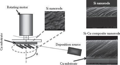
FIGURE 49.1 The fabrication of Si and Cu-Si alloy nanostructures using the approach of oblique angle deposition. Deposition sources of Si and Cu can be selected to synthesize the composite nanowires.
49.2.2 OBLIQUE ANGLE CODEPOSITION OF CU-SI
The fabrication of the Cu3Si nanowires can be conducted by an oblique angle (co)deposition technique [19, 20 and 21] in a two-source electron-beam deposition system, where two quartz crystal microbalances (QCMs) can be installed to monitor the near-normal deposition thickness and rate of each source independently [4]. The OAD method is simply a physical vapor deposition (VPD) technique in which flux arrives at a large oblique incidence angle (> 80°) from the substrate normal (while the substrate is rotating), as shown schematically in Figure 49.1. This results in the formation of isolated nanorods by the self-shadowing effect during growth. Either pure Si or Cu-Si nanowires can be codeposited on the Cu film-coated glass substrates at a vapor incident angle of α with respect to the substrate normal. PVD methods such as sputtering and e-beam evaporation are clean and repeatable, have high deposition rates, and can be grown over large areas with good adhesion to the substrate. OAD provides a convenient method to grow Cu-Si nanorods by using the additional Cu deposition source [4].
49.3 CHARACTERIZATION OF CU SILICIDE NANOWIRES
49.3.1 SELF-ASSEMBLED NANOWIRES
Since the self-assembly of Cu-Si nanowires has not been widely studied, the crystalline structure was studied to identify the type of Cu-Si that is formed. We have also investigated the influence of the surface preparation on the growth mode. Cu-Si nanowires grown on clean and oxidized Si surfaces were compared. The nanowires (or nanoislands) were randomly formed on the Si substrate and located using an in situ SEM and are shown in Figure 49.2. Figure 49.2a shows a low-magnification view after a typical fabrication process. Similar to experiments on Ag nanowires described in Refs. [12, 13 and 14], the length rather than the width increases with deposition time. Some of the nanoislands were observed to have pyramidal shapes with truncated tops, whereas the rest of the nanoislands had undefined shapes, as seen in Figure 49.3.
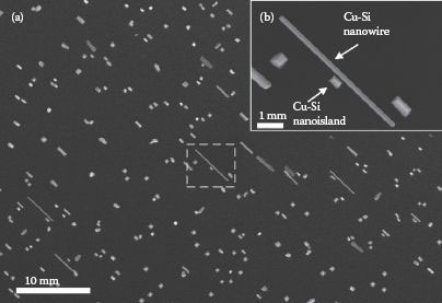
FIGURE 49.2 An in situ SEM image of Cu-Si nanowires and nanoislands with (a) a low-magnification view and the dashed box is shown with (b) a high-magnification view.
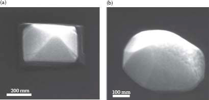
FIGURE 49.3 Ex situ SEM images taken with a 52° tilt using the FEI Nova 600 Dual Beam system. (a) A Cu-Si nanopyramid with a truncated top. (b) An irregularly shaped nanoisland. (P. K. Ng et al. Self assembled Cu nanowires on vicinal Si(001) by the E-beam evaporation method, Presented at the 11th IEEE International Conference on Nanotechnology (IEEE-NANO), Portland, OR. © (2011) IEEE. With permission.)
49.3.2 GROWTH CHARACTERISTICS OF SELF-ASSEMBLED NANOWIRES
To investigate the structural properties of the nanowires in three dimensions, cross-sectional SEM images were obtained. These cross sections were prepared by FIB ion-milling. Two randomly chosen Cu-Si nanowires were ion-milled to reveal their cross-sectional shapes, as shown in Figure 49.4. The cross-sectional ex situ SEM images show that the two Cu-Si nanowires do not have well-defined facets. The cross-sectional dimensions for the nanowires in Figure 49.4a and b are the following: widths are 210 and 295 nm, respectively; thicknesses are 93 and 100 nm, respectively; and height of the nanowires measured between the peak of the nanowire and the surface of Si substrate are 50 and 50 nm, respectively. Also, the Cu-rich material extends into the substrate, indicating severe interdiffusion (indicated by dashed lines). To show the differences between Ag and Cu-Si more clearly, we also fabricated and analyzed Ag nanowires. The resulting SEM image is shown in Figure 49.5. As found in Refs. [12, 13 and 14], the Ag nanowire has a well-defined trapezoidal cross-sectional shape and is more uniform than the two Cu-Si nanowires observed in Figure 49.4. Furthermore, the Ag does not significantly extend into the Si substrate. Rather, some Si “wetting” toward the Ag nanowire seems to have taken place. In contrast, little or no Si wetting toward Cu-Si nanowires is seen at the edges of the two Cu-Si nanowires in Figure 49.4.
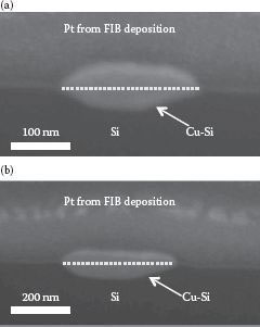
FIGURE 49.4 Cross-sectional view of the ex situ SEM images, (a) and (b), of two different Cu–Si nanowires tilted at 52° prepared by using an FIB. Although both nanowires in (a) and (b) were fabricated on the same Si substrate, the two nanowires do not exhibit similar cross section shape and geometry. Each Cu–Si nanowire in (a) and (b) had undefined and irregular facets. The dashed lines portray the imaginary Si surface’s plane. (P. K. Ng et al. Self assembled Cu nanowires on vicinal Si(001) by the E-beam evaporation method, Presented at the 11th IEEE International Conference on Nanotechnology (IEEE-NANO), Portland, OR. © (2011) IEEE. With permission.)
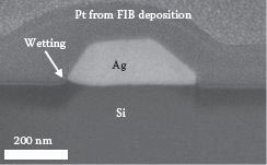
FIGURE 49.5 Cross-sectional view of the ex situ SEM image of a Ag nanowire tilted at 52° prepared by using an FIB. (P. K. Ng et al. Self assembled Cu nanowires on vicinal Si(001) by the E-beam evaporation method, Presented at the 11th IEEE International Conference on Nanotechnology (IEEE-NANO), Portland, OR, P. K. Ng et al. High resolution analysis of self assembled Cu nanowires on vicinal Si(001), Presented at the 11th IEEE International Conference on Nanotechnology (IEEE-NANO), Portland, OR. © (2011) IEEE. With permission.)
The different degrees of interdiffusion might be explained by Ag-Si [22] and Cu-Si phase diagrams [18]. Ag and Si do not form silver silicide (Ag-Si) even at the deposition temperature of 600 °C. In contrast, Cu-Si diffusion occurs well below 600°C. Indeed, Cu-Si interdiffusion has been confirmed with the STEM experiments discussed below. In another set of experiments, we have investigated the effect of the Si surface quality on the growth of Cu-Si nanowires. The e-beam evaporation procedure was exactly the same as before. The only difference was that the Si surface was not flash-treated, and thus the native oxide was present during the e-beam evaporation process. The resulting morphology is shown in Figure 49.6a. The fuzzy appearance of the image is caused by the poor electrical conductivity of SiO, which leads to charging and affects the SEM performance. A lower density of Cu-Si nanowires was observed than without a native oxide. In addition, the nanowire labeled with “A” in Figure 49.6a shows that some Cu-Si nanowires exhibit an inhomogeneous cross section. Obviously, the left side of the nanowire “A” is wider than the right side. Again, details of the cross section were obtained from the cross-sectional TEM shown in Figure 49.6b. The width of the nanowire amounts to 150 nm and the height to 220 nm. It is not known what causes the different contrast in the figures.
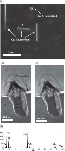
FIGURE 49.6 Cu-Si nanowires on an Si substrate with native oxide. (a) An ex situ SEM view with a 52° tilt, (b,c) a cross-sectional TEM view, and (d) XEDS analysis showing the presence of O, Si, and Cu in the nanowire. The element Mo is from the TEM grid. (P. K. Ng et al. Self assembled Cu nanowires on vicinal Si(001) by the E-beam evaporation method, Presented at the 11th IEEE International Conference on Nanotechnology (IEEE-NANO), Portland, OR, © (2011) IEEE. With permission.)
Figure 49.6c shows the outline of the nanowire in dashed lines. The shape is very different from the Cu-Si nanowires grown on clean Si. The oxide material on the Si surface obviously modifies the growth mechanism, possibly through a higher surface diffusion barrier. The horizontal dashed line indicates the imaginary surface plane of the Si substrate. It is obvious that the Cu nanowire interdiffuses with the Si substrate even though there is an oxide barrier. Although this mechanism is currently not understood, it is believed that the Cu atoms can penetrate through the thin and porous layer of the native oxide at the annealing temperature of 600°C. Nevertheless, details of the growth mechanisms require further studies. The preliminary x-ray energy-dispersive spectrometer (XEDS) experiments shown in Figure 49.6d reveal that the material is composed of Cu, Si, and O. Further research is also needed to determine the exact material composition and phase.
49.3.3 HIGH-RESOLUTION ANALYSIS OF SELF-ASSEMBLED CU SILICIDE NANOWIRES
TEM diffraction pattern tests were performed on nanowires to determine their crystalline structures. Two Cu-Si nanowires from the same substrate are labeled as “Cu-Si wire 1” and “Cu-Si wire 2,” as shown in Figures 49.7a and 49.8a. In the right panels of these figures are the local diffraction patterns. They reveal that wire 1 possesses a single crystalline structure. In contrast, wire 2 is composed of two grains with a low-angle boundary between them. The two low-angle Cu grains appear to have a projected rotational mismatch of 3° based on the projection of the Si[110] zone axis, which is shown in Figure 49.9. It is important to note that this measured angle is derived from the Si[110] zone projection. It is possible that the two low-angle grains may actually be slightly rotated along another arbitrary axis that is close to the Si[110] axis. The reason for the formation of the two different structures is presently unknown. However, the hexagonal patterns obtained from the two diffraction patterns strongly indicate an epitaxial relationship between the Cu-Si nanowires and the Si substrate.
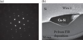
FIGURE 49.7 Single crystalline, self-assembled Cu-Si nanowires with (a) their diffraction pattern obtained from TEM analysis and (b) a cross-sectional view prepared by FIB. (P. K. Ng et al. High resolution analysis of self assembled Cu nanowires on vicinal Si(001), Presented at the 11th IEEE International Conference on Nanotechnology (IEEE-NANO), Portland, OR. © (2011) IEEE.)
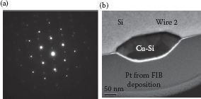
FIGURE 49.8 Low-angle grain boundary, self-assembled Cu-Si nanowires with (a) their diffraction pattern obtained from TEM analysis and (b) a cross-sectional view prepared by FIB. (P. K. Ng et al. High resolution analysis of self assembled Cu nanowires on vicinal Si(001), Presented at the 11th IEEE International Conference on Nanotechnology (IEEE-NANO), Portland, OR. © (2011) IEEE.)
FIGURE 49.9 Indexed Si[110] zone pattern. (P. K. Ng et al. High resolution analysis of self assembled Cu nanowires on vicinal Si(001), Presented at the 11th IEEE International Conference on Nanotechnology (IEEE-NANO), Portland, OR. © (2011) IEEE. With permission.)
To study the chemical composition of the wires, two nanowires were selected as shown in Figure 49.10a. The nanowire with a triangular top is labeled as “A” while the other nanowire with a flat top is labeled as “B.” An FIB-TEM analysis was performed on these two nanowires. The TEM images of nanowires “A” and “B” are shown in Figure 49.10b and c. The dashed lines in Figure 49.10b and c illustrate the original surface plane of the Si substrate. The reason for this observation may be Cu-Si diffusion during the 600°C annealing process since diffusion occurs at this temperature [18].
STEM energy z-contrast images were obtained for the two nanowires, as shown in Figure 49.11a and b. The numeric labels in the figures are the locations of the XEDS spectra that were measured. Elemental analysis data are shown in Figure 49.11c. From these XEDS data, we find discrete Cu:Si ratios of roughly 50:50, 30:70, and 70:30. Indeed, Cu3Si is a stable phase [18]. However, the other Cu-Si phases with ratios 50:50 and 30:70 are not known to be stable after annealing to 600°C [18]. Future studies are needed to understand the existence of unstable Cu-Si phases in the Cu-Si nanowires.
In summary, an in-depth discussion is presented here on the synthesis and material characteristics of self-assembled Cu-Si nanowires. The self-assembly method may not be the ideal method for integrating Cu-Si nanowires to Li-ion nanowires. However, the methods do enable the synthesis of ideal Cu-Si nanowires (i.e., single crystalline or with a few defects and contaminant free) that can be characterized for electrical and defect tolerance that is necessary for fundamental research as Li-ion anode materials. Furthermore, in situ electrical characterization can be performed after the selfassembling Cu-Si nanowires in the UHV environment without exposure to the ambient impurities, which are currently being studied. In the following section, the synthesis of Cu-Si nanowires as a Li-ion anode will be discussed. Although the synthesis techniques are different, the characterization of the material properties is complementary to study the fundamental properties of Cu-Si nanowires and select the ideal crystalline structure, doping and Cu-Si phase properties, and dimensions.
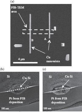
FIGURE 49.10 (a) SEM image of self-assembled Cu-Si nanowires that appeared to have an “A” triangular top surface and a “B” regular flat top surface. Cross-sectional view of the FIB-TEM area in (a) for (b) a regular top “B” wire and (c) a triangular top “A” wire. (P. K. Ng et al. High resolution analysis of self assembled Cu nanowires on vicinal Si(001), Presented at the 11th IEEE International Conference on Nanotechnology (IEEE-NANO), Portland, OR. © (2011) IEEE. With permission.)
49.3.4 CHARACTERIZATION OF (CO)DEPOSITED CU SILICIDE NANOWIRES
Both the pure Si and Cu-Si composite nanorods were fabricated by an oblique angle (co)deposition technique in a custom-designed, two-source electron-beam deposition system, where two QCMs were installed to monitor the near-normal deposition thickness and rate of each source independently [23,24]. During the anode nanostructure fabrication, first, a layer of a 200-nm-thick Cu film was coated onto the 10 × 30 mm glass substrates as the current collector of battery anodes at a deposition rate of rCu = 0.2 nm/s. Then, Cu-Si alloy nanowires were deposited on the Cu film-coated glass substrates at a vapor incident angle of α = 88° and both Cu and Si sources were coevaporated at rCu = 0.5 nm/s and rSi = 0.4 nm/s. The mass of the active Si on an area of 10 × 30 mm was estimated to be approximately 3.7 × 10⁻⁵ g for the Cu-Si alloy nanowires.
The codeposited samples consist of arrays of well-aligned and tilted Si and Cu-Si nanowires (Figure 49.1). The x-ray diffraction (XRD) results in Figure 49.12 show that the as-deposited Si nanowires are amorphous (Figure 49.12a); however, when codeposited with Cu, a polycrystalline orthorhombic Cu3Si phase forms, as revealed by the peak Cu3Si (012) at 2θ ≈ 44.57° in Figure 49.12. In the TEM images, the amorphous Si matrix and the high-contrast Cu3Si nanoparticles can be seen. This indicates that the Cu-Si nanowires are composed of the polycrystalline Cu3Si nanoparticles embedded in the amorphous Si nanowire matrix. The nanoparticles are estimated to have diameters of ~3–5 nm.
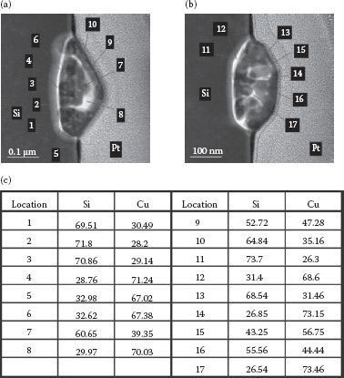
FIGURE 49.11 STEM z-contrast data for (a) wire “A” and (b) wire “B,” where the numeric labeled locations of the spot analyses were performed. (c) EDX data where the atomic percentages of Si and Cu are given for the locations in (a) and (b). (P. K. Ng et al. High resolution analysis of self assembled Cu nanowires on vicinal Si(001), Presented at the 11th IEEE International Conference on Nanotechnology (IEEE-NANO), Portland, OR. © (2011) IEEE. With permission.)
49.4 CU SILICIDES AS LI-ION ANODE MATERIALS
To study the lithiation behavior of Cu-Si nanowires, the nanowires fabricated via OAD were subjected to a charging process inside a TEM [25,26]. The applied bias voltage was set to be −2 V on a Cu-Si nanowire to drive Li-ions into the nanowire. Figure 49.13 shows the structural evolution of a Cu-Si nanowire as a function of charging time. As expected, the diameter of a nanowire increases during Li-ion intercalations in the anode nanowire. From Figure 49.13a and b, one can observe the change of diameter from 173 to 201 nm upon 15 min of charging. In addition, the formation of high-contrast nanoparticles was detected, which can be related to various LixSi alloys. According to Figure 49.13c, the diameter of the Cu-Si alloy nanowire increases much faster during the lithiation process in comparison to the pure Si nanowires. This indicates that alloying Si with Cu and the Cu3Si crystals can improve the rate of lithiation.
The lithiation performance of single crystals of Cu3Si nanowires is expected to be superior to that of the amorphous Cu-Si alloys. The electrical conductivity of Cu3Si single crystals is greater than the low electrical conductivity of amorphous Cu-Si alloys. Prior results have shown that the metallic Cu3Si nanowires are excellent conductors with a resistivity of less than 30 μΩ⋅cm [11]. In addition to the better electronic conductivity, the single crystalline nature of the nanowires will be ideal to prevent localized lithiation and delithiation, which may result in the premature fracture of the nanowires. In fact, our previous results [25] show that lithiation can be surface diffusion dominant and the selective locations on the surface can be the predominant place for the lithiation process. The single crystalline structure of the Cu3Si nanowires can promote a uniform diffusion path for the Li-ions to transfer into the crystal structure and interact with the host atoms.
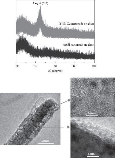
FIGURE 49.12 (Top) XRD patterns of the deposited (a) Si and (b) Cu-Si composite nanowires. (Bottom) The TEM images of the Cu-Si nanowire indicate the presence of crystalline Cu3Si embedded in an amorphous matrix. (From Journal of Power Sources, 196, M. Au et al., Silicon and silicon–copper composite nanorods for anodes of Li-ion rechargeable batteries, 9640–9647, Copyright 2011, with permission from Elsevier.)
In summary, we have briefly discussed the fabrication methods for single-crystal and Cu-alloyed amorphous Si nanowires. Although the synthesis technique for single-crystal nanowires cannot be directly integrated into anode material for Li-ion batteries, these nanowires enable fundamental studies of the properties needed for Cu-Si nanowire anode materials. It is expected that single crystalline Cu-Si nanowires will provide lower electrical resistivity and better surface Li ion diffusion than the alloyed Si nanowires due to their uniformity in crystalline structure. This will prevent localized lithiation/delithiation found in the OAD Cu-Si nanowires that may result in the formation of cracks and fractures of the nanowires. Further work is needed on synthesizing freestanding single crystalline Cu-Si nanowires for in situ TEM lithiation/delithiation studies and on improving the crystalline structure of the OAD nanowires.
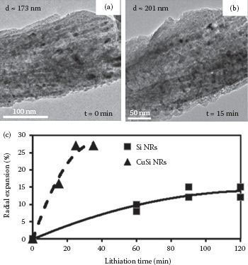
FIGURE 49.13 (a) A Cu-Si nanowire just before the start of the lithiation process. The diameter is around 173 nm. (b) The same Cu-Si nanowire after 15 min of the lithiation process and the diameter increased to 201 nm. (c) The graph compares the radial expansion of Cu-Si and pure Si nanowires as a function of lithiation time. The Cu-Si alloy nanowire shows a higher rate of mechanical straining, which indicates that the rate of charging is faster for a Cu-Si nanowire.
C. M. Lilley acknowledges the support from the National Science Foundation (Award No. 846814, Division of Civil, Mechanical and Manufacturing Innovation). The use of the Center for Nanoscale Materials was supported by the U.S. Department of Energy, Office of Science, Office of Basic Energy Sciences, under Contract No. DE-AC02-06CH11357. C.M.L. would also like to acknowledge the technical assistance from Dr. Ke-Bin Low of the Research Resource Center at the University of Illinois at Chicago in the TEM characterization of the self-assembled Cu-Si nanowires and Dr. Alexandra Joshi-Imre from the Center for Nanoscale Materials for her assistance in the TEM sample preparation. In addition, C.M.L. thanks Mr Brandon Fisher for his technical assistance on the Omicron system at the Center for Nanoscale Materials. Finally, C.M.L. acknowledges the contribution to the growth mechanics analysis by Dr. Matthias Bode at the University of Wuerzburg.
R. S. Yassar acknowledges the support from the National Science Foundation (Award No. 0820884, Division of Materials Research) and the American Chemical Society—Petroleum Research Fund (Award No. 51458-ND10). R.S.Y. also recognizes the contributions from Dr. Ming Au at the Savannah River National Laboratory for the preparation of Cu-Si nanostructures and the XRD characterization. Also, thanks to Dr. Hessam Ghassemi at Drexel University for the in situ microscopy of the Cu-Si alloy nanostructures.
1. M. Armand and J. M. Tarascon, Building better batteries, Nature, 451, 652–657, 2008.
2. M. Green, E. Fielder, B. Scrosati, M. Wachtler, and J. S. Moreno, Structured silicon anodes for lithium battery applications, Electrochemical and Solid State Letters, 6, A75–A79, 2003.
3. U. Kasavajjula, C. Wang, and A. J. Appleby, Nano- and bulk-silicon-based insertion anodes for lithium-ion secondary cells, Journal of Power Sources, 163, 1003–1039, 2007.
4. M. Au, Y. He, Y. Zhao, H. Ghassemi, R. S. Yassar, B. Garcia-Diaz, and T. Adams, Silicon and silicon–copper composite nanorods for anodes of Li-ion rechargeable batteries, Journal of Power Sources, 196, 9640–9647, 2011.
5. L. Baggetto, R. A. H. Niessen, F. Roozeboom, and P. H. L. Notten, High energy density all-solid-state batteries: A challenging concept towards 3D integration, Advanced Functional Materials, 18, 1057–1066, 2008.
6. J. Yang, M. Winter, and J. O. Besenhard, Small particle size multiphase Li-alloy anodes for lithium-ion batteries, Solid State Ionics, 90, 281–287, 1996.
7. H. Föll, H. Hartz, E. Ossei-Wusu, J. Carstensen, and O. Riemenschneider, Si nanowire arrays as anodes in Li ion batteries, Physica Status Solidi (RRL)—Rapid Research Letters, 4, 4–6, 2010.
8. J. P. Maranchi, A. F. Hepp, A. G. Evans, N. T. Nuhfer, and P. N. Kumta, Interfacial properties of the a-Si/Cu: Active–inactive thin-film anode system for lithium-ion batteries, Journal of the Electrochemical Society, 153, A1246–A1253, 2006.
9. C. K. Chan, H. Peng, G. Liu, K. McIlwrath, X. F. Zhang, R. A. Huggins, and Y. Cui, High-performance lithium battery anodes using silicon nanowires, Nature Nanotechnology, 3, 31–35, 2008.
10. H. Qiaojian, C. M. Lilley, R. Divan, and M. Bode, Electrical failure analysis of Au nanowires, IEEE Transactions on Nanotechnology, I, 7, 688–692, 2008.
11. S. J. Jung, T. Lutz, A. P. Bell, E. K. McCarthy, and J. J. Boland, Free-standing, single-crystal Cu3Si nanowires, Crystal Growth & Design, 12(6), 3076–3081, 2012.
12. K. R. Roos et al., High temperature self-assembly of Ag nanowires on vicinal Si(001), Journal of Physics: Condensed Matter, 17, S1407, 2005.
13. Q. Huang, C. M. Lilley, and M. Bode, Surface scattering effect on the electrical resistivity of single crystalline silver nanowires self-assembled on vicinal Si (001), Applied Physics Letters, 95, 103112–103113, 2009.
14. B. Stahlmecke, F. J. M. z. Heringdorf, L. I. Chelaru, M. H.-v. Hoegen, G. Dumpich, and K. R. Roos, Electromigration in self-organized single-crystalline silver nanowires, Applied Physics Letters, 88, 053122-3, 2006.
15. P. K. Ng, B. Fisher, K. B. Low, A. Joshi-Imre, M. Bode, and C. M. Lilley, Comparison between bulk and nanoscale copper-silicide: Experimental studies on the crystallography, chemical, and oxidation of copper-silicide nanowires on Si(001), Journal of Applied Physics, 111, 104301–104307, 2012.
16. P. K. Ng, B. Fisher, M. Bode, and C. M. Lilley, Self assembled Cu nanowires on vicinal Si(001) by the E-beam evaporation method, Presented at the 11th IEEE International Conference on Nanotechnology (IEEE-NANO), Portland, OR, 2011.
17. P. K. Ng, B. Fisher, K. B. Low, A. Joshi-Imre, M. Bode, and C. M. Lilley, High resolution analysis of self assembled Cu nanowires on vicinal Si(001), Presented at the 11th IEEE International Conference on Nanotechnology (IEEE-NANO), Portland, OR, 2011.
18. H. Okamoto, Cu-Si (copper-silicon), Journal of Phase Equilibria, 23, 281–282, 2002.
19. R. Teki, N. Koratkar, T. Karabacak, and T.-M. Lu, Enhanced photoemission from nanostructured surface topologies, Applied Physics Letters, 89, 193116–3, 2006.
20. Y. P. Zhao, D. X. Ye, G. C. Wang, and T. M. Lu, Novel nano-column and nano-flower arrays by glancing angle deposition, Nano Letters, 2, 351–354, 2002.
21. K. Robbie, J. C. Sit, and M. J. Brett, Advanced techniques for glancing angle deposition, Journal of Vacuum Science & Technology B: Microelectronics and Nanometer Structures, 16, 1115–1122, 1998.
22. Ag-Si, Journal of Phase Equilibria, 10, 673–674, 1989.
23. Y. He, Z. Zhang, C. Hoffmann, and Y. Zhao, Embedding Ag nanoparticles into MgF2 nanorod arrays, Advanced Functional Materials, 18, 1676–1684, 2008.
24. Y. He, J. Fan, and Y. Zhao, The role of differently distributed vanadium nanocatalyst in the hydrogen storage of magnesium nanostructures, International Journal of Hydrogen Energy, 35, 4162–4170, 2010.
25. H. Ghassemi, M. Au, N. Chen, P. A. Heiden, and R. S. Yassar, In situ electrochemical lithiation/delithiation observation of individual amorphous Si nanorods, ACS Nano, 5, 7805–7811, 2011.
26. H. Ghassemi, M. Au, N. Chen, P. A. Heiden, and R. S. Yassar, Real-time observation of lithium fibers growth inside a nanoscale lithium-ion battery, Applied Physics Letters, 99, 123113–123113, 2011.