
High-Aspect-Ratio Metallic Nanowires by Pulsed Electrodeposition |
CONTENTS
50.2.2 Electrodeposition of Ag NWs
50.3.3 NW Deposition by DC Plating
50.3.4 NW Deposition by Pulsed Plating
50.3.5 The Need for High-Aspect-Ratio NWs: Pathway to Packaging at Nanoscale
50.3.6 Deposition Mechanism during Pulsed Electroplating into Pores
Since the miniaturization and the performance increase of electronic components nowadays are ongoing parallel trends in the microelectronics industry, the introduction of nanometer (nm)-scale materials emerges even in the field of packaging, and interconnections within the back-end-of-line (BEoL) processes are also subjects of these processes [1]. Their potential as thermally, mechanically, or electrically enhancing additive to established packaging materials reduces their potential to a passive role. The use of carbon nanotubes (CNTs) inside Cu-based through-silicon vias (TSVs) [2,3] or packaging polymers [4,5] are prominent examples. On the other hand, the use of one-dimensionally elongated nanoparticles featuring a high aspect ratio (AR, the ratio of particle length to diameter), so-called nanowires (NWs) gains more and more attention when it comes to an active, that is, interconnecting incorporation of nanoparticles into packaging [6, 7 and 8]. Their mostly bottom-up-based fabrication has already been realized by versatile approaches [9]. In general, one-dimensional growth can be achieved either by energetically favored growth based on high crystal structure anisotropy of the growing material or by spatial confinement during growth achieved by a template with parallel pores of a defined geometry. In the latter case, this geometry determines the later geometry of the NWs, that is, their diameter, length, and order. Diameters in the range of a few nanometers up to several hundred nanometers have already been achieved using different template materials. Among mesoporous silica [10], track-etched polycarbonate [11], or self-organizing block copolymers [12], anodically oxidized alumina (AAO) [13, 14 and 15] enables beneficial features for template-assisted NW synthesis. AAO offers a wide range of variable pore geometries (pore diameters from 25 to 500 nm, interpore distances from 50 to 400 nm, pore depths from a few nanometers to micrometers, depending on the thickness of the Al used) while enabling once tremendous pore densities up to 1011 pores/cm2, through-going and nearly defect-free pores, and a very high degree of hexagonal pore order. Pores of AAO templates have been successfully filled with metals [16, 17 and 18], metallic alloys [19], or (conductive) polymers [20], demonstrating the high material versatility for AAO-assisted NW synthesis. Different architectures, such as core–shell structures [21], multisegmented NWs [22], or nanoporous NWs [23], have also been obtained by filling the pores of AAO templates.
Similar to the manifoldness in materials used for NW synthesis are the methods for pore filling. Among, for example, chemical deposition [24] or monomer injection followed by polymerization [25], electrodeposition of the desired NW species is the most common method to fabricate metalbased NWs. As depicted in Figure 50.1e, electrochemical deposition can be once potential driven or otherwise controlled by the applied current, which forces the deposition reaction. In this sense, the first mode applies a thermodynamic force to the system, whereas the current-driven mode—the most common for electrochemical deposition—enables kinetic control simply by the current used for deposition. Since—as a consequence of the ongoing deposition reaction—the properties (i.e., the resistance, R) of the system electrolyte–surface change drastically with time, one of the two parameters current, i, or potential, E, has to change as the other is kept constant by a galvanostat or potentiostat, respectively. When depositing under constant current conditions (amperostatic), the cell potential can reach regions in which the NW deposition is not favored thermodynamically and side reactions (e.g., the evolution of gases and the decomposition of the deposited species) occur and disturb the deposition reaction. When applying a thermodynamic force (in the case of potential-driven deposition) to the system, the growth does not show linear behavior anymore but more regularity with time. From the kinetic point of view, a reductive deposition reaction proceeds much faster than the diffusion of ions to the pore bottom through thin and long pores. Consequently, the deposition is highly controlled by diffusion. To enable the diffusion process to level the concentration of the electrolyte at the electrochemical double layer (EDL) of the cathode (pore bottom) to the concentration inside the bulk of the above-standing electrolyte, a deposition pause after the deposition enables the diffusion to take place. In this pause (which is much longer than the deposition period itself), no reaction apart from the diffusion shall be allowed. Such pulsed deposition processes are known to lead to much more homogenous deposits with a smaller grain size [26]. In this chapter, we focus on the pulsed electrodeposition of Ag into the pores of AAO with the objective of gaining higher NW homogeneity, faster NW growth, and an evaluation of growth kinetics. In the concluding section, we substantiate the need for higher ARs within the use of NW arrays for an anisotropically conductive and adhesive NW film acting as a fine pitch interconnecting layer, for example, for vertical three-dimensional or flip-chip interconnection applications.
AAO templates used for these investigations were fabricated as reported elsewhere [14] and schematized in Figure 50.1. High-purity (99.999%) Al foils were purchased from ABCR, Germany. Al pretreatment included ultrasonic degreasing twice, alternating in ethanol and acetone, followed by a 2 h vacuum annealing step (p < 10−3 mbar, T = 500°C), and an electropolish (48 V, T = 20°C, ethanol−HClO4–methylcellulose 1:4:1 per volume). Anodic oxidation was carried out in a two-step process (40 V DC, 2°C under stirred oxalic acid). First, anodization was conducted for 4 h, followed by a stripping step (T = 60°C, stirring in 5 wt.-% H3PO4 and 1.8 wt.-% CrO3, 2 h) to dissolve the first porous layer of Al2O3. The second anodization was carried out under the same conditions as the first, but for 10 h (Figure 50.1b), resulting in a pore depth of approximately 20 μm. Then the carrying Al was dissolved from the backside using a mixture of CuCl2 and concentric HCl for 15 min (Figure 50.1c). A closed thin layer (thickness ~200 nm) of Au was sputtered onto the front side of the gained membrane (Figure 50.1d). For electrodeposition, the pores on the backside were opened by dipping the membrane into 0.3 M NaOH for 5 min. Pores were finally widened using 5 wt.-% H3PO4 for 15 min.
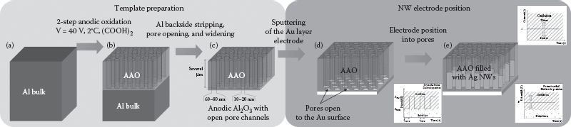
FIGURE 50.1 Schematic procedure of the AAO template-assisted electrodeposition of Ag NWs: (a) Starting from high-purity bulk Al; (b) continuing over a two-step anodization and generation of a regularly ordered pore structure; (c) stripping the remaining carrier Al layer and opening/widening the pores; (d) after sputtering a con-tinuous thin layer of Au onto one surface acting as the cathode layer while performing electrodeposition inside the pores under different deposition.
50.2.2 ELECTRODEPOSITION OF AG NWS
To evaluate the deposition potential, cyclic voltammetry (CV) was carried out with the Ag(I)containing electrolyte (2.3 M KSCN, 0.1 M Ag2SO4, pH ~6) onto a flat Au surface. Electrodeposition was carried out according to Riveros et al. [16]. For sufficient wetting of the AAO pores with the electrolyte, substrates were exposed to the electrolyte solution for at least 30 min prior to the deposition. All depositions were done using a PC-controlled potentiostat by Princeton Applied Research. Potentiostatic deposition was carried out under DC conditions for 30 min at room temperature and a cathodic deposition potential of −250 mV versus standard calomel electrode (SCE) as reference and a flat Pt counterelectrode (CE). Potential-pulsed deposition was carried out for different pulse frequencies, f, as defined by
(50.1) |
Thereby, the total time for one pulse and pause (tpulse + tpause) was kept constant at 1 s throughout all experiments. For growth homogenization, the corresponding potentials (all vs. SCE) were varied between Epulse = −250 mV with Epause = 0 mV and Epulse = −320 mV with Epause = −220 mV. For the evaluation of NW growth kinetics, pulsed deposition was carried out for 5, 10, 20, and 30 min.
Scanning electron microscopy (SEM) was carried out with a ZEISS Supra 40VP equipped with a backscatter electron-sensitive detector enabling a higher material contrast. Electrochemical impedance spectroscopy (EIS) was performed using a Gamry potentiostat in the frequency range of 1 Hz to 1 MHz with −10 mV cathodic bias, a 135 nm Au layer evaporated onto Al as a working electrode (WE), a Pt sheet as CE, and SCE as a reference electrode (RE). Nyquist plot’s semicircle fit in Figure 50.3h was performed by parabolic mathematical fits.
As shown in Figure 50.2a, the pores of AAO can be estimated to have a diameter of around 60–70 nm and an interpore distance of 100–110 nm. The pores can be estimated to grow in depth with a velocity of about 2 μm/h of anodization, giving easy control over pore depth.
From the cathodic current occurring in the cyclovoltammogram of Figure 50.2b, the reductive potential region (i.e., i < 0 mA) of the used electrolyte can be estimated to lie between −220 and −350 mV followed by cathodic currents related to other decomposition reactions inside the electrolyte. In the anodic potential region, a strong anodic current related to the oxidative dissolution of the deposited Ag can be observed.
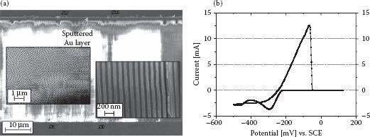
FIGURE 50.2 (a) SEM picture of an empty AAO template (second anodization 20 h) with a thin Au layer visible on top. Left inset: Top view onto hexagonal pore arrangement after second anodization. Right inset: Magnified picture of parallel pore channels after pore widening of 30 min. (b) Cyclovoltammogram of a 0.1 M Ag2SO4 + 2.3 M KSCN electrolyte on Au surface (starting from 0 mV into cathodic region with 50 mV/s).
50.3.3 NW DEPOSITION BY DC PLATING
According to CV results, DC plating was performed at E = −250 mV (vs. SCE) since the highest cathodic current appears at this point. Results are shown in Figure 50.3a and c. Ag NW growth could be obtained with nearly 100% lateral filling degree in AAO. The current measured during deposition shows a slight decrease with time after a long initiation period of approximately 200 s of seed growth on the pore bottoms. The slight current decrease with ongoing deposition is related to the decreasing concentration of the electrolyte in the EDL region according to Faraday’s law. Theoretically, this is compensated weakly by the slowly decreasing length of the diffusion path through the pores since they are filled with time and the deposition region shifts toward the AAO upside. Apart from that, these NWs are observed to be rather inhomogeneous in length with a relative standard deviation of 13% so that we expected pulsed plating as an option to level the NW length.
50.3.4 NW DEPOSTION BY PULSED PLATING
In pulse plating experiments, the two most important parameters are pulse frequency, f, and pulse/pause potentials. Apart from that, we have investigated the influence of Ag+ concentration on the homogeneity of the NW precipitate. Figure 50.3b shows the results of a deposition with f = 0.01 and pulse potentials same as in the DC deposition experiment (i.e., Epulse = −250 mV, Epause = 0 mV). It is obvious that the NWs are very inhomogeneous in structure, length, and filling. This is mostly related to the long deposition pauses. When switching to 0 mV, the system crosses the oxidative potential region (compare Figure 50.3) so that strong dissolution effects occur. To avoid the dissolution during pulse pauses, we chose a pause potential that causes no significant effect (i.e., no pause current) in the system. SEM pictures of samples where a pause potential of Epause = −220 mV and a deposition potential Epulse = −320 mV were applied for deposition are shown in Figure 50.3d–f. No traces of dissolution can be observed in these figures. Apart from that, since the filling degree is related to seed growth that is higher with increased seed concentration, the strong influence of Ag(I) concentration on pore filling can be observed when comparing Figure 50.3d with Figure 50.3e. Figure 50.3g shows the time evolution of the deposition current during pulse plating with Epause = −220 mV and Epulse = −320 mV. The inset explains the attributed curves that evolve due to the high resolution of measurement. Three conclusions can be made from these curves: (1) The pause current of nearly 0 mA during pulsed plating proves that there is actually no significant process occurring, which is connected to a Faraday conversion during deposition pauses. (2) Pulse currents are about two orders of magnitude higher compared to DC plating, resulting in much longer NWs than obtained by DC plating in 30 min. To evaluate the growth rate during pulsed plating, we performed electrodeposition under f = 0.05, c = 0.1 mM, Epulse = −320 mV, and Epause = −220 mV for 5, 10, 20, and 30 min. (3) The pulse current curve shows an increase in the deposition current starting at approximately 22 min. This might be attributed to the fast increasing NW length, which reduces the diffusion path through the pores and leads to a faster deposition. This stands in agreement with the nonlinear growth behavior indicated in Figure 50.5. Figure 50.3f shows small NWs with an average length of 1.42 ± 0.07 μm and very high regularity obtained after 5 min of electrodeposition. Figure 50.3h shows a graph of time-dependent NW length evolution. It is obvious that NW growth by pulsed plating is not linear with time, which we expected and explained before. Apart from that, an increase in standard deviation (the absolute standard deviation is indicated by the error bars) with time can be observed, but compared with the relative standard deviation (DC: 13.0%, pulsed plating: 6.2%; each after 30 min), a considerable decrease in length inhomogeneity can be observed by optimized pulse plating.
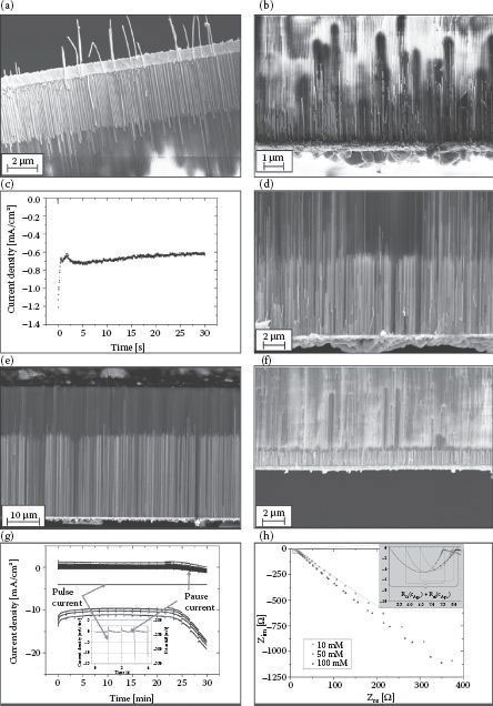
FIGURE 50.3 Results of Ag electrodeposition into pores of AAO: (a) NWs obtained by 30 min DC plating at E = −250 mV with corresponding time-current density developing (c); NWs obtained by pulse plating for 30 min with f = 0.01, c = 0.05 mM, and Epulse = −250 mV, Epause = 0 mV (b), with f = 0.05, c = 0.05 mM, Epulse = −320 mV, and Epulse = −220 mV (d), with f = 0.05, c = 0.1 mM, Epulse = −320 mV, and Epulse = −220 mV (e; inset shows material composition obtained by energy dispersive x-ray spectroscopy [EDS]) with corresponding time-current density development (g; inset shows a magnification of the different deposition curves) and with f = 0.05, c = 0.1 mM and, Epulse = −320 mV, Epulse = −220 mV after 5 min (f). (h) EIS results (Nyquist plot) of the Ag2SO4/2,3 M KSCN electrolyte at a flat Au electrode in dependence of Ag+ concentration with a magnified inset indicating RC semicircle behavior at high frequencies (fitted by parabolic function, distance between roots represents the ohmic resistance for charge transfer at the Au surface) without Warburg impedance/constant phase element.
50.3.5 THE NEED FOR HIGH-ASPECT-RATIO NWS: PATHWAY TO PACKING AT NANOSCALE
The obtained NW arrays being embedded in AAO are planned to be applied as vertically interconnecting layers inside flip-chip or three-dimensionally stacked architectures as described before [6] and depicted in Figure 50.4. As experienced, a very thin layer of AAO is mechanically very brittle. Consequently, to realize such a described film with vertically oriented NWs, a sufficient film thickness is important for later lamination processability in chip-to-chip (C2C), chip-to-wafer (C2W), or wafer-to-wafer (W2W) assembly processes. Since the NWs shall interconnect both sides of the film, their length is determined by the lowest applicable film thickness, which is assumed here to be in the range of 10–20 μm. This refers to NW ARs of 140–280 (assuming NW diameters of 70 nm). To gain these values by simple DC plating, very long deposition times have to be accepted. With pulse plating, these ARs can be realized in much shorter times and higher regularity. Apart from that, the NWs in the film are also expected to act as a mechanically enhancing agent, that is, they provide higher film flexibility as they are longer.
The NW film is expected to show various beneficial features when applied as a chip-interconnecting film. Among them, the reduction of the effective signal transporting cross section from a currently established solder microball to numerous (~103) thin metallic NWs enables the elimination of the frequency-limiting skin effect (since the skin thickness is more than the NW diameter, NWs do not suffer a reduction of transmission cross section). Apart from that, the laterally highly resolved NWs fit present as well as future demands of contact geometries and provide electrically contacted neighbored to noncontacted NWs, which can (because of their metallic nature) act as thermally trapping devices and so contribute to the reduction of thermal stress in densely packed chip stacks.
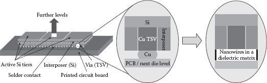
FIGURE 50.4 Application scheme for high-aspect-ratio metallic NWs embedded in an AAO matrix. The filled membrane shall be applied within vertical packaging either between two active Si chips in 3D chip stacks or—as depicted—for direct vertical interconnection from a chip/TSV interposer to the printed circuit board (PCB).
50.3.6 DEPOSITION MECHANISM DURING PULSED ELECTROPLATING INTO PORES
From the kinetic NW growth curve in Figure 50.5, three distinct observations can be made: First, the growth can be significantly accelerated and pushed toward higher length homogeneity by applying pulsed electrodeposition. Second, the filling of nanoscale pores by pulsed electrodeposition is no linear process since the NW length obviously does not increase linearly with time and is better fitted by a parabolic function. Third, the speed of NW growth seems to be dependent on pore depth since the 30 min point (40 μm membrane thickness) is not well fitted by the curve made up by 20 μm membrane points. To understand the reasons for all the three observations made, we hereby formulate a qualitative deposition mechanism.
When observing the time-current transients of the one pulse–pause sequence, one notices in both a current decay from a very high peak value to a much lower end value. When fitting the much longer pause behavior mathematically, one would suggest a single exponential decay that is corresponding to the typical decharging behavior of a capacitor. This capacitor can be the EDL between an Au electrode and an electrolyte, which is decharged when positive charge carriers are reduced at the electrode surface. EIS measurements (see Figure 50.3h) on the system of a blank Au electrode facing the same electrolyte as used in the pulsed pore electrodeposition experiments described above showed that the system cannot be described by this simple model, but rather by a more complex system such as suggested in Figure 50.6 involving the intrinsic resistance of the electrolyte itself, the charge transfer resistance (depending on the Ag+ concentration in the electrolyte), and a supposedly Warburg, or more general, a constant phase element impedance that can be caused by a diffusive barrier in front of the blank electrode [27]. This is obvious since there is no typical semicircle behavior but a continuous increase in phase shift between the potential and the current. Diffusively caused Warburg impedance would then cause a slope with an angle α of 45° between real part impedance, Zre, and imaginary part impedance, Zim. Since the observed slope is higher, this additive impedance can more generally be characterized by the model of a constant phase element.
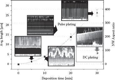
FIGURE 50.5 Kinetic growth curve of Ag NWs grown in AAO templates by constant potential electroplating (DC plating) and pulsed potential electroplating with SEM pictures, which were the basis for NW length measurement. The electrolyte was of the same composition in all cases. AAO template membranes were 20 μm in thickness for 5, 10, and 20 min and 40 μm for pulse and DC plating samples after 30 min each. Error bars represent the relative deviation in length with respect to the measured average length.
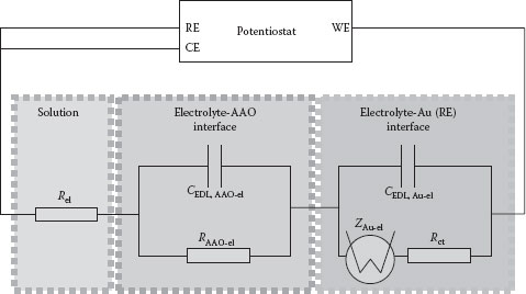
FIGURE 50.6 Equivalent electrical circuit diagram corresponding to AAO pore deposition with the following elements: Rel, the intrinsic electrical resistance of the electrolyte, RAAO-el and CEDL, AAO-el, the capacitance of the EDL between the AAO surface and the electrolyte, CEDL, Au-el, the EDL capacitance of the double layer between the Au cathode and the electrolyte, ZAu-el, the constant phase element’s impedance of the Au cathode (as observed by EIS) and Rct, the electrical resistance of the cathodic charge transfer process at the Au electrode; RE, the reference electrode (SCE), CE, the counterelectrode (Pt), and WE, the working electrode.
By adding a membrane with thin pores in front of this electrode, convective acceleration of the diffusion is avoided actively, depending on the pore length, so that with longer pores, the diffusion path for the electrolyte increases. In contrast, it decreases as long as the pores are being filled, and the cathode surface (e.g., the top of the NW, the place where the growth proceeds) is more or less slowly shifted to the membrane’s top, which so reduces the diffusion length again. In addition to this, Chien et al. predict that a second EDL is added in a series circuit to the Au-electrolyte, resulting in a proposed equivalent electrical circuit as depicted in Figure 50.6 [28]. Further investigations on the particular assembly of the AAO-EDL to the Au-EDL will follow. We now cannot surely predict whether the equivalent circuitry represents the complete sum of all electrical elements involved in the electrochemical deposition process. Also, a possible influence of the pore geometry cannot be evaluated, yet. Since the range of influences of surface effects, such as superviscosity causing very high friction coefficients at the nanoscale, is—to the best of our knowledge—not further characterized for the system of AAO pores, we cannot predict a possible threshold of pore width/length where pore diffusion is significantly hindering the electrolyte from diffusing to the electrode [29].
In this chapter, we have demonstrated the feasibility of generating high-aspect-ratio metallic NWs by enhanced pulse plating of Ag into highly ordered pores of AAO. We have shown once a significant increase in NW length and AR (DC: 56, pulsed plating: 373), respectively, within the same time of deposition (30 min) and a decrease of length inhomogeneity when performing pulsed electrodeposition. The parameters being evaluated and expected to have the most significant influence on the deposition process were pulse frequency, Ag(I) concentration, as well as pulse and pause potential. When choosing a pause potential too high, strong dissolution effects during the pauses cause very high inhomogeneity of the NWs. The effect of faster and denser NW growth with higher Ag+ concentration was proven. NW growth kinetics were recorded and showed a continuous but nonlinear behavior in growth rate. In future, the obtained NW arrays shall be used inside an anisotropically conductive interconnecting film featuring vertically aligned NWs that have to feature higher ARs for better film processability. We sketched a qualitative model for the nanopore-confined electrochemical NW growth featuring electrical elements (such as a Warburg impedance at the Au cathode), which will be further characterized by EIS measurements.
The authors gratefully acknowledge V. Haehnel and H. Schlörb from the Leibniz-Institute for Solid State and Materials Research (IFW) Dresden, J. Katzmann and T. Härtling from the Fraunhofer Institute for Non-Destructive Testing Dresden (IZFP-D), as well as the Technische Universität Dresden’s Young Researchers Training Group “Nano- and Biotechnologies for Electronics Packaging” (DFG 1401/1) for technical guidance.
1. Roadmap by ITRS, Issue 13: Assembly & Packaging, pp. 56–58, 2009.
2. Y. Chai, K. Zhang, M. Zhang, P. C. H. Chan, and M. M. F. Yuen, Carbon nanotube/copper composites for via filling and thermal management, IEEE Proc. Elec. Components Tech. Conf. (ECTC), 2007.
3. M. Fayolle et al., Integration of dense CNTs in vias on 200 mm diameter wafers: Study of post CNT growth processes, IEEE Proc. Int. Interconn. Tech. Conf. (IITC), 2011.
4. M. Heimann, B. Boehme, S. Scheffler, M. Wirts-Ruetters, and K.-J. Wolter, CNTs—A comparable study of CNT-filled adhesives with common materials, IEEE Proc. Elec. Components Tech. Conf. (ECTC), pp. 1871–1878, 2009.
5. B. Li, Y.-C. Zhang Z.-M. Li S.-N. Li, and X.-N. Zhang, Easy fabrication and resistivity-temperature-behaviour of an anisotropically conductive carbon nanotube-polymer composite, J. Phys. Chem. B, 114(2), 689–696, 2010.
6. M. Graf et al., Nanowire filled polymer films for 3D system integration, IEEE Proc. Int. Interconn. Tech. Conf. (IITC) 2011, pp. 1–3.
7. K. J. Ziegler et al., Conductive films of ordered nanowire arrays, J. Mater. Chem., 14, 585–589, 2004.
8. R.-J. Lin et al., Design of nanowire anisotropic conductive film for fine pitch flip chip interconnection, IEEE Proc. 6th Electr. Pack. Tech. Conf. (EPTC), pp. 120–125, 2004.
9. Y. Xia et al., One-dimensional nanostructures: Synthesis, characterization, and applications, Adv. Mater., 15(5), 353–389, 2003.
10. F. Schüth, Non-siliceous mesostructured and mesoporous materials, Chem. Mater., 13, 3184–3195, 2001.
11. C. Schonenberger et al., Template synthesis of nanowires in polycarbonate membranes: Electrochemistry and morphology, J. Phys. Chem. B, 101, 5497–5505, 1997.
12. M. Stamm, S. Minko, I. Tokarev, A. Fahmi, and D. Usov, Nanostructures and functionalities in polymer thin films, Macromol. Symp., 214, 73–83, 2004.
13. C. R. Martin, Nanomaterials—A membrane-based synthetic approach, Science, 266, 1961–1966, 1994.
14. O. Jessensky, F. Müller, and U. Gösele, Self-organized formation of hexagonal pore arrays in anodic alumina, Appl. Phys. Lett., 72(10), 1173–1175, 1998.
15. A. P. Li, F. Müller, A. Birner, K. Nielsch, and U. Gösele, Hexagonal pore arrays with 50–420 nm interpore distance formed by self-organization in anodic alumina, J. Appl. Phys., 84(11), 6023–6026, 1998.
16. G. Riveros et al., Silver nanowire arrays electrochemically grown into nanoporous anodic alumina templates, Nanotechnology, 17(2), 561–570, 2006.
17. H. Cao, L. Wang, Y. Qiu, and L. Zhang, Synthesis and properties of aligned copper nanowires, Nanotechnology, 17(6), 1736–1739, 2006.
18. A. J. Yin, J. Li, W. Jian, A. J. Bennett, and J. M. Xu, Fabrication of highly ordered metallic nanowire arrays by electrodeposition, Appl. Phys. Lett., 79(7), 1039–1041, 2001.
19. V. Haehnel, C. Mickel, S. Fahler, L. Schultz, and H. Schlörb, Structure, microstructure, and magnetism of electrodeposited Fe70Pd30 nanowires, J. Phys. Chem. C, 114(45), 19278–19283, 2010.
20. D. J. Shirale, M. A. Bangar, W. Chen, N. V. Myung, and A. Mulxhandani, Effect of aspect ratio (length:Diameter) on a single polypyrrole nanowire FET device, J. Phys. Chem. C, 114(31), 13375–13380, 2010.
21. P. R. Evans, W. R. Hendren, R. Atkinson, and R. J. Pollard, Nickel-coated gold-core nanorods by template assisted electrodeposition, J. Electrochem. Soc., 154(9), K79–K82, 2007.
22. F. Gao and Z. Gu, Nano-soldering of magnetically aligned three-dimensional nanowire networks, Nanotechnology, 21(11), 115604–115610, 2010.
23. C. Ji and P. C. Searson, Fabrication of nanoporous gold nanowires, Appl. Phys. Lett., 81(23), 4437–4439, 2002.
24. Z. Hu, T. Xu, R. Liu, and H. Li, Template preparation of high density, and large-area Ag nanowire arrays by acetaldehyde reduction, Mater. Sci. Eng. A, 371236–371240, 2004.
25. H. Masuda and K. Fukada, Ordered metal nanohole arrays made by a two-step replication of honeycomb structures of anodic alumina, Science, 268, 1466–1468, 1995.
26. N. Kanani, Electroplating—Basic Principles, Processes and Practice, 1st ed., Elsevier, Amsterdam, pp. 117–124, 2004.
27. E. Barsoukov, Impedance Spectroscopy—Theory, Experiment and Applications, 2nd ed., Wiley Interscience, Hoboken, NJ, pp. 85–88, 2005.
28. M.-C. Chien, G.-J. Wang, and W.-C. Yu, Modelling ion diffusion current in nanochannel using infinitesimal distribution resistor-capacitor circuits, Jpn. J. Appl. Phys., 46(11), 7436–7440, 2007.
29. S. Guriyanova, V. G. Mairanovsky, and E. Bonaccurso, Superviscosity and electroviscous effects at an electrode/aqueous electrolyte interface: An atomic force microscope study, J. Coll. Interface Sci., 360(2), 800–804, 2011.