
CONTENTS
52.3.1 Effect of Concentration of Zn Solution on the Formation of ZnO Nanorods
52.3.2 XRD and PL Spectra of ZnO Nanorods
52.3.3 I–V Characteristics of the Undoped (n-type) and N-Doped (p-type) Nanorods Grown on n-type PS
One-dimensional (1D) materials have stimulated much attention due to their promising potential in extensive applications [1]. The recent research in this field focuses on investigating the dependence of electrical transport and optical and mechanical properties on size and dimensionality [2,3]. Among them, semiconducting zinc oxide (ZnO), which has a wide bandgap of 3.37 eV and a large exciton binding energy of 60 meV, has attracted much attention due to its promising potential as a “future material” [4]. At ambient pressure and temperature, ZnO crystallizes in the wurtzite structures, as shown in Figure 52.1. This is a hexagonal lattice and is characterized by two interconnecting sublattices of Zn2+ and O2−, such that each Zn ion is surrounded by tetrahedral O ions and vice versa. This tetrahedral coordination gives rise to polar symmetry along the hexagonal axis. This polarity is responsible for a number of properties of ZnO, including its piezoelectricity and spontaneous polarization, and is also a key factor in crystal growth, etching, and defect generation. Many groups have focused on novel nanostructures with different shapes ranging from nanowires to nanobelts and even nanosprings. ZnO nanorods or nanowires are generally synthesized by four main techniques: chemical vapor deposition [5], metal–organic vapor deposition [6], aqueous solution method (equal to chemical bath deposition (CBD)) [7], and electrodeposition [8].
In spite of the many studies on the ZnO synthesis on various substrates [9,10] or porous templates [11,12], ZnO nanorod films grown on porous silicon (PS) have been little studied. PS is one of the most important Si-based materials because its open structure and large surface area, combined with unique optical and electrical properties, make it a challenging position for templates [13,14]. PS is a very promising material due to its excellent mechanical and thermal properties, obvious compatibility with silicon-based microelectronics, and its low cost. The large surface area within a small volume, combined with controllable pore sizes, convenient surface chemistry, and the ability to modulate its refractive index as a function of depth, makes PS a suitable dielectric material for the formation of a multilayer.
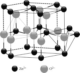
FIGURE 52.1 Wurtzite structure model of ZnO.
Alternatively, as-grown ZnO is typically n-type, and different hypotheses have been proposed to explain n-type conductivity [15]. The achievement of reproducible p-type ZnO still remains one of the significant obstacles to wide applications of ZnO in a p–n junction device. Thus, the n- or p-type ZnO grown on n-type PS using the CBD method offers a cheap route for an application to various p–n junction devices. We adopted the atomic layer deposition (ALD) technique to make seed layer for p-type ZnO nanorods. ALD is a chemical gas-phase, thin-film deposition method based on alternate saturative surface reactions. In ALD, the source vapor is pulsed into the reactor alternately, one at a time, separated by purging or evacuation periods. Each precursor exposure step saturates the surface with a monomolecular layer of that precursor. This results in a unique self-limiting growth mechanism with a number of advantageous features, such as good conformality and uniformity, and accurate film thickness control.
In this chapter, ZnO nanorod films are synthesized on a PS template using the CBD technique. We demonstrate that the conductivity type (n- or p-type) of ZnO nanorods can be changed by controlling the seed layer preparation. Two types of seed layers are prepared by ALD with/without nitrogen (N) doping.
The PS layer was made by the electrochemical anodization method on an n-type Si (100) wafer. The Si substrate has a resistivity of 1–20 ohm⋅cm. Al (100 nm) was deposited on the back side of the substrate to form an electrode as an anode and the Pt plate was served as a cathode (counterelectrode). Electrochemical anodization was carried out for 20 min in a Teflon cell containing HF:ethanol:deionized (DI) water = 1:2:1 volume ratio with 50 mA/cm2 current densities. A 50 W halogen lamp was used for the back side illumination for derivation of effective holes during electrochemical anodization. The resultant PS layer has a thickness of about 20–30 µm. After the anodization process, the substrate was rinsed with DI water and dried in a nitrogen atmosphere.
ZnO seed layers were prepared on the PS surface from diethylzinc (DEZn, Zn 52.0%, Aldrich) and H2O precursors, and nitrogen (N) doping was achieved by NH3 gas. Typical sequences for growing with the N-doped and non-N-doped ZnO seed layers were [DEZn/Ar/H2O/Ar/NH3/Ar] 2/10/2/10/3/15 sec and [DEZn/Ar/H2O/Ar] 1/5/2/7 sec, respectively. The process was repeated for the formation of the ZnO layer up to 20 nm in depth inside the PS. The role of Ar was to remove the residual diethylzinc inside the reaction chamber so as not to react with the next H2O precursor. The working pressure was 0.3 Torr and Ar gas was used as a carrier gas and purging gas with a flow rate of 50 sccm. The temperature of the PS substrate was kept at 423.15 K.
The synthesis of the ZnO nanorod films was carried out by the CBD method. Plastic bottles were filled with a mixture a of 0.02 M equimolar aqueous solution of zinc nitrate hexahydrate ((Zn(NO)3)2⋅6H2O) and hexamethylenetetramine (HMT; C6H12N4). Subsequently, the ZnO seed layer-grown PS substrates were placed in the bottles and heated at a constant temperature of 343.15 K for 24 h. As-grown ZnO nanorod films were washed with DI water to eliminate residual salts, dried in air, and annealed at 673.15 K to enhance the crystallinity. An annealing process was essential to remove the residual organic material and improve the crystallinity of the ZnO nanorods. The crystalline character and doping state of the samples were examined via x-ray diffraction (XRD) and photoluminescence (PL) spectroscopy, respectively. Au electrodes were fabricated using the magnetron sputtering method on each side of the sample to measure the electrical properties. Two samples (n-type ZnO or p-type ZnO on n-type PS) were investigated throughout the measurement of the forward and reverse bias I–V curve.
52.3.1 EFFECT OF CONCENTRATION OF ZN SOLUTION ON the FORMATION OF ZNO NANORODS
We confirmed the effect of concentration of Zn solution (zinc nitrate and hexamethylenetetraamine equimolecular solution) on the formation of ZnO nanorods on an Si wafer. Figure 52.2 shows FE-SEM images of the product resulting from the aqueous chemical growth of ZnO obtained by a further lowering of the overall concentration of the precursors to the low millimolar range. A seed layer of ZnO with 20 nm thickness was deposited by using RF sputtering. Crystalline nanorods, about 100–400 nm in diameter and up to 1–2 µm long, were identified at various concentrations of the Zn solution after 40 h of aging. When the reaction time was constant, the diameter of the ZnO nanorod was decreased and adjacent nanorods were coalesced as the concentration of the solution increased.
52.3.2 XRD AND PL SPECTRA OF ZNO NANORODS
The scanning electron microscopy (SEM) images of the ZnO nanorods prepared with different seed layers are shown in Figure 52.3. The geometric parameters for growing rods such as growth time and solution composition were the same for two samples as described in the experimental section. We can observe that the N-undoped seed layer yields smaller nanorods (Figure 52.3a and b) and the N-doped seed layer by NH3 gas yields larger nanorods (Figure 52.3c and d). N-doping would affect the seed layer density.
Figure 52.4 shows the XRD patterns of the N-undoped and N-doped ZnO nanorod films on an n-type PS substrate. The XRD was operated at the condition of 40 kV and 100 mA with Cu Kα line radiation. The major peaks of the samples are identified and compared with JCPDS file 36-1451. This reveals that two samples are composed of hexagonal ZnO with lattice constants a = 0.325 nm and c = 0.522 nm, and have a hexagonal wurtzite crystalline ZnO structure. The (002) peak of the N-doped ZnO nanorods implies better alignment than undoped ZnO nanorods. The higher intensity of the (002) peak for the sample indicates that the ZnO nanorods are perpendicularly oriented to the substrate. To evaluate the mean crystallite size of two samples, Scheerer’s formula is adopted [16]. The mean crystallite size of two samples corresponds to 36, 41, and 32 nm for the (110), (002), and (101) directions, respectively, which means that the crystallite growth is slightly faster along the c axis direction.
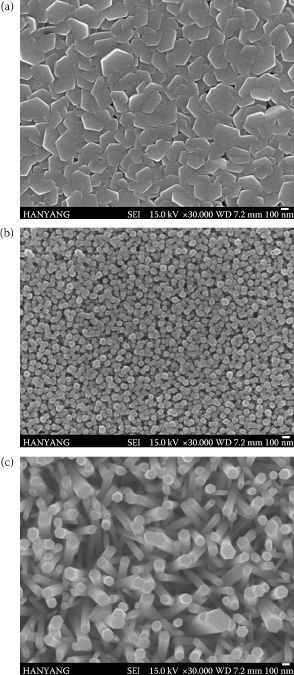
FIGURE 52.2 SEM images showing differences of ZnO nanorod’s formation grown on Si wafers by dipping in ZnO solutions with a concentration of (a) 0.1 M, (b) 0.05 M, and (c) 0.02 M.
Figure 52.5 shows the room-temperature PL spectra of the N-undoped and N-doped ZnO nanorods grown on the n-type PS substrate. The peak (380–415 nm) emerging at the visible range of the N-undoped sample results from the near-band-edge emission. Blue light emission appears at 460 nm, which is predicted from intrinsic defects such as zinc and oxygen interstitials produced through the annealing process. The effect of N-doping is confirmed from the result of the PL spectra. Compared to the N-undoped ZnO nanorods, N-doped ZnO nanorods show the red shift phenomenon. N-doping leads to the increase of internal hole concentration inside the ZnO nanorods; thus, the bandgap of the N-doped ZnO nanorods becomes narrower.
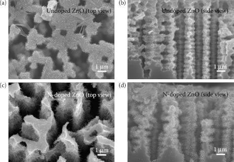
FIGURE 52.3 SEM images of the ZnO nanorod: (a) top and (b) side view images of the N-undoped ZnO nanorods on PS (n-type ZnO/n-type PS), (c) top and (d) side view images of the N-doped ZnO nanorods on PS (p-type ZnO/n-type PS).
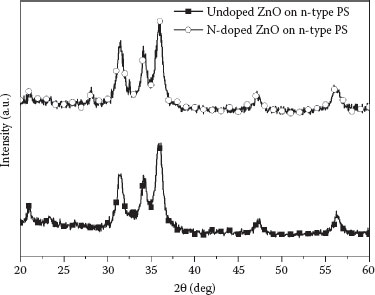
FIGURE 52.4 XRD patterns of the undoped and N-doped ZnO nanorod films.
52.3.3 I −V CHARACTERISTICS OF the UNDOPED (N-TYPE) AND N-DOPED (p-TYPE) NANORODS GROWN ON N-TYPE PS
To study whether N-doping effectively changes the carrier type of the N-doped ZnO nanorods, we compare the I–V characteristics of the N-undoped and N-doped ZnO nanorods grown on n-type PS. The I–V characteristics of the N-undoped and N-doped ZnO nanorods on n-type PS are measured at room temperature. Figure 52.6 clearly shows that the N-undoped ZnO nanorods (n-type ZnO nanorods) do not form a rectifying diode with the n-type PS. However, the N-doped ZnO nanorods (p-type ZnO nanorods) form a good rectifying diode with an n-type PS. These results clearly indicate that the N-doping process achieved via NH3 gas during the seed layer formation changes the carrier type of the ZnO nanorods from n-type to p-type semiconducting materials.
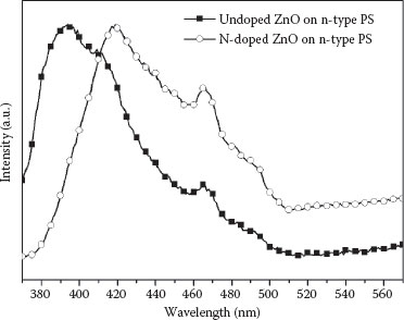
FIGURE 52.5 Room-temperature PL spectra of the N-undoped and N-doped ZnO nanorods on an n-type PS.
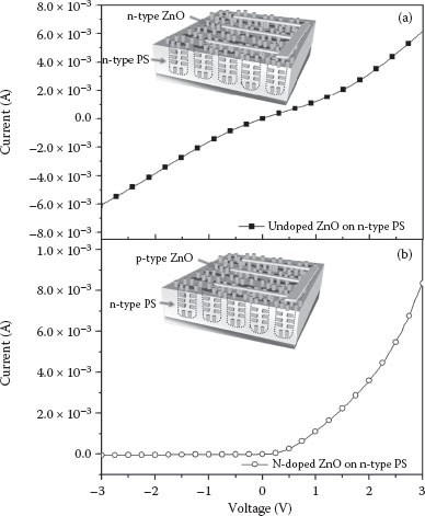
FIGURE 52.6 I–V characteristics of (a) undoped (n-type) and (b) N-doped ZnO nanorods (p-type) grown on an n-type PS.
Well-directed ZnO nanorods are grown on n-type PS substrates via CBD. N-type ZnO nanorods are changed to p-type by the N-doping process achieved by NH3 gas during the formation of seed layers. The N-doped ZnO nanorod (p-type ZnO nanorod) films can form a good p–n heterojunction with the n-type PS substrate.
This study was supported by the National Research Foundation of Korea funded by the Ministry of Education, Science, and Technology (2011-0028850, 2011-0027329, and 2011-0003056).
1. Y. N. Xia, P. D. Yang, Y. G. Sun, Y. Y, Wu, B. Mayers, B. Gates, Y. D. Yin, F. Kim and H. Yan, One-dimensional nanostructures: Synthesis, characterization and application, Adv. Mater., 15, 353–389, 2003.
2. M. S. Gudiksen, L. J. Lauhon, D. C. Smith and C. M. Lieber, Growth of nanowire superlattice structures for nanoscale photonics and electronics, Nature, 415, 617–620, 2002.
3. Y. Haung, X. F. Daun, Y. Cui, L. J. Lauhon, K. H. Kim and C. M. Libber, Logic gates and computation from assembled nanowire building blocks, Science, 294, 1313–1317, 2001.
4. C. W. Bunn, The lattice-dimensions of zinc oxide, Proc. Phys. Soc., 47, 835–842, 1935.
5. R. S. Wagner and W. C. Eliss, Vapor-liquid-solid mechanism of single crystal growth, Appl. Phys. Lett., 4, 89–90, 1964.
6. W. Lee, M. C. Heong and J. M. Myoung, Evolution of the morphology and optical properties of ZnO nanowires during catalyst-free growth by thermal evaporation, Nanotechnology, 15, 1441–1445, 2004.
7. A. Dricil, G. Djeteli, G. Tchangbedji, H. Ferouiche, K. Jondo, K. Napo, J. C. Bernede, S. Ouro-Djobo and M. Gbagba, Structured ZnO thin films grown by chemical bath deposition for photovoltaic applications, Phys. Stat. Sol. A, 201, 1528–1536, 2004.
8. M. A. Verges, A. Mifsud and C. J. Serna, Formation of rod-like zinc oxide microcrystals in homogeneous solutions, J. Chem. Soc. Farad. Trans., 86, 959–963, 1990.
9. H. J. Ko, Y. F. Chen, Z. Zhu, T. Yao, I. Kobayashi and H. Uchiki, Photoluminescence properties of ZnO epilayers grown on CaF2.(111) by plasma assisted molecular beam epitaxy, Appl. Phys. Lett., 76, 1905–1907, 2000.
10. A. Ohtomo, K. Tamura, K. Saikusa, T. Takahashi, T. Makino, Y. Segawa, H. Koinuma and M. Kawasaki, Single crystalline ZnO films grown on lattice-matched ScAlMgO4(0001) substrate, Appl. Phys. Lett., 75, 2635–2637, 1999.
11. W. H. Zhang, J. L. Shi, L. Z. Wang and D. S. Yan, Preparation and characterization of ZnO clusters inside mesoporous silica, Chem. Mater., 12, 1408–1413, 2000.
12. Y. Li, G. W. Meng, L. D. Zhang and F. Phillipp, Ordered semiconductor ZnO nanowire arrays and their photoluminescence properties, Appl. Phys. Lett., 76, 2011–2013, 2000.
13. D. C. Look, Progress in ZnO materials and devices, J. Electron. Mater., 35, 1299–1305, 2006.
14. Q. Ahsanulhaq, A. Umar and Y. B. Hahn, Growth of aligned ZnO nanorods and nanopencils on ZnO/Si in aqueous solution: Growth mechanism and structural and optical properties, Nanotechnology, 18, 115603-1–110503-7, 2007.
15. M. Caglar, S. Ilican and Y. Caglar, Influence of dopant concentration on the optical properties of ZnO: In films by sol-gel method, Thin Solid Films, 517, 5023–5028, 2009.
16. B. D. Cullity, Elements of X-Ray Diffraction (Addison-Wesley, Reading, MA, 1978), p. 10.