
High-Speed and Transparent Nanocrystalline ZnO Thin Film Transistors |
CONTENTS
54.2 Thin Film Deposition and Device Fabrication
54.3.2 Influence of Growth Temperature
54.4.3 Transparent Transistors
Thin film transistors (TFTs) made from amorphous or organic semiconductors are commonly used in the control circuits of large-area display electronics such as flat-panel TV screens. They can also be used in applications requiring flexible or nonplanar surfaces where the use of regular single crystal electronics is problematic. The usefulness of TFTs, however, has not been extended to high-performance applications due to significantly inferior electronic properties of thin films compared to their single crystal counterparts. For example, the field-effect electron mobility of amorphous Si is typically 0.1 cm2/V.s, whereas the mobility values in single crystal Si can be in excess of 1000 cm2/V.s [1]. Metal-oxide semiconductors based on Zn, In, Ga, and Hf have shown great promise in solving these problems for the current and next-generation flat-panel display electronics [2,3]. However, most metal-oxide semiconductor thin films are also amorphous and have limitations in current density and switching on/off ratios. Although they offer higher electron mobilities than amorphous Si films and therefore show promise in higher-speed circuit applications [4], they are not yet suitable for high-performance digital or analog circuits beyond display control electronics.
The bonding in ZnO and similar oxide semiconductors is strongly ionic and the states near the conduction band minimum arise almost completely from cation (zinc) s-orbitals. This is in strong contrast to covalent or near-covalent semiconductors like Si or GaAs where the sp-bonding is sensitive to both the bond angle and bond length disorder that easily generates localized states (traps). In ZnO, the nearly spherical and relatively large, empty zinc cation orbitals that form the conduction band result in electron transport that is largely unaffected by the bond angle or bond length disorder, and the disorder does not result in localized states [5]. It is anticipated that radiation-induced damage will have minimal effect on electronic device operation due to this insensitivity to lattice disorder [6]. Initial results show that ZnO TFTs and circuits have remarkable tolerance to high-dose gamma ray and neutron radiation and that damages caused by irradiation can be removed by low-temperature annealing [7].
Because ZnO is also a wide bandgap semiconductor, it can be used for both transparent contact layers and the channel semiconductor in transparent electronics applications. We have shown that high-performance transparent transistors can be fabricated using only nc-ZnO films and no indiumcontaining layers.
In this report, a comprehensive study of the nc-ZnO thin film growth conditions was undertaken to understand the factors influencing the film properties as they relate to the transistor operation. The influence of the gate dielectric material on the physical properties of ZnO films and the transistor performance was identified. Device design issues related to the high-frequency (microwave) operation were identified and approaches used to mitigate these issues were described.
Ordered nc-ZnO thin films composed of closely packed nanocolumns offer a unique solution to improving TFT performance to levels comparable to single crystal semiconductors while maintaining their thin film properties. High-speed transistors were fabricated using 1.2–2 µm gate length devices with cut-off frequencies as high as 10 GHz [8].
Thin films of spontaneously ordered and closely packed nanocolumns of ZnO were used to fabricate high-speed and transparent TFTs. The use of nanocrystalline ZnO (nc-ZnO) helps to achieve the intrinsic electronic properties of single crystals while providing substrate agnostic thin films that can be grown on nonplanar surfaces of rigid or flexible substrates. We have developed low-temperature pulsed laser deposition (PLD) techniques for both doped and undoped nc-ZnO films and demonstrated microwave transistor operation (fmax = 10 GHz). Unlike in amorphous TFTs, the operation of nc-ZnO transistors relies on field-effect charge control at vertical grain boundaries between nanocolumns and can produce very high on/off ratios (>1012), very high current densities, and near-ideal subthreshold voltage swings (~74 mV/decade). Using a combination of doped and undoped nc-ZnO films, we have fabricated the first indium-free transparent TFTs with excellent performance and transparency.
54.2 THIN FILM DEPOSITION AND DEVICE FABRICATION
Nc-ZnO films were deposited in a Neocera Pioneer 180 pulsed laser deposition system with a KrFexcimer laser (Lambda Physik COMPex Pro 110, λ = 248 nm, 10 ns pulse duration). The following processing conditions were used to deposit undoped ZnO films for active layers of transistors: laser energy density of 2.6 J/cm2, laser repetition rate of 30 Hz, deposition temperature of 25–400°C, oxygen partial pressure of 1–100 mTorr during the deposition, and substrate-to-target distance of 9.5 cm. The target was a 50 mm diameter by 6 mm thick sintered ZnO ceramic disk (99.999%). The deposition parameters for conductive transparent ZnO films (used as contact layers in transparent transistors) were the same, except that Ar gas was used during deposition instead of oxygen [9] and the source material was high-purity ZnO with 3% Ga2O3 used as an n-type dopant. Various gate insulators, including SiO2, Al2O3, and HfO2, were used in this study. SiO2 films were grown in a PlasmaTherm 790 plasmaenhanced chemical vapor deposition (PECVD) system at 250°C. Al2O3 and HfO2 films were prepared in a Cambridge Nanotech Fiji F200 atomic layer deposition (ALD) system at 150–250°C.
The ZnO crystal structure was determined by using a PANalytical X’Pert Pro MRD x-ray diffractometer. Film morphologies were analyzed with an FEI DB235 scanning electron microscope (SEM) and a JEOL 4000EX transmission electron microscope (TEM) operating at 400 kV. Surface roughness was measured with a Veeco Dimension 3000 atomic force microscope (AFM). Dielectric film thickness and refractive index were measured with a Horiba JobinYvon UVISEL spectroscopic ellipsometer. Optical transmission measurements were made with a Varian Cary 5000 spectrophotometer.
Devices for low-frequency characterization were fabricated on p-type Si wafers or flexible polyimide films. The gate lengths, LG, were varied from 2 to 25 µm. High-speed devices were fabricated on high-resistivity Si substrates (>2000 ohm.cm) to minimize capacitive parasitics. Gate lengths for these devices varied from 1.2 to 3 µm.
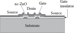
FIGURE 54.1 Cross-sectional schematic of the baseline nc-ZnO thin film transistor. (B. Bayraktaroglu and K. Leedy, 2011 11th IEEE International Conference on Nanotechnology, August 15–18, Portland, Oregon, pp. 1450–1455. © (2011) IEEE. With permission.)
Transparent devices were fabricated on quartz or glass substrates. A bottom-gate configuration was used for all transistors, where the gate contact was fabricated first directly on the substrate. As shown in Figure 54.1, the gate contact is covered with the gate insulator and the nc-ZnO film is produced conformably over the gate insulator. The Ni/Au and Ti/Au contacts were used as the gate and the source/drain contacts for the nontransparent devices, whereas the Ga-doped ZnO (GZO) films were used as contacts for the transparent devices. Other device-processing details were reported elsewhere [3].
The source and drain contacts overlap the gate contact by 0.5–3 µm. To reduce the parasitic capacitance effects due to this overlap of gate and source–drain contacts for high-frequency devices, a thicker gate insulator was used in these regions while maintaining a thinner gate insulator under the channel region. In this way, high transconductance was maintained while reducing the effects of parasitic elements. The gate length is defined as the distance between the source and drain contacts. No intentional surface passivation was applied to the free surface of the ZnO film.
Cross-sectional TEM images of ZnO films deposited conformably over the gate contact indicate that the film is composed of densely compacted, highly faulted columnar-shaped grains that predominantly extend through the thickness of the film, as shown in Figure 54.2. The nanocolumnar grain diameters were in the 20–50 nm range depending on the film growth parameters such as substrate temperature and oxygen pressure, but self-ordering of nanocolumns was observed with films grown on other types of gate insulators also, as shown in Figure 54.3.
X-ray diffraction scans of the ZnO films deposited on the SiO2, Al2O3, and HfO2 gate dielectrics exhibited a highly textured c-axis orientation with only the ZnO (002) peak present, consistent with other studies of PLD ZnO films [10, 11, 12 and 13]. The RMS surface roughness of ZnO films deposited on SiO2 and HfO2 was 0.65 and 0.94 nm, respectively, as measured by AFM. AFM images in Figure 54.4 also show slightly larger ZnO grains grown on HfO2 compared to SiO2 in agreement with the cross-sectional TEM results. The measured surface roughness of the underlying dielectric material was approximately 0.2 nm, regardless of the film composition, deposition technique, or deposition temperature. This smooth surface was necessary for the ordered ZnO grain growth and produced a well-defined dielectric–ZnO interface, which was essential for device performance.
54.3.2 INFLUENCE OF GROWTH TEMPERATURE
At deposition temperatures of <75°C, the grains exhibited diffraction contrast differences and, in some areas, nearly equiaxed grain structures. As the film growth temperature increased from 100°C to 400°C, films displayed an increasingly uniform columnar grain structure and consistent diffraction contrast. With increasing deposition temperature up to 400°C, the intensities of the ZnO (002) peak increased and full-width at half-maximum values of the ZnO (002) decreased, as shown in Figure 54.5a, indicating improved film crystallinity. The 2Θ positions were less than the 34.421° 2Θ (002) peak from the JCPDS #36–1451 powder diffraction file indicating strained lattice structures. Progressively higher ZnO (002) peak intensities were obtained from ZnO films deposited on HfO2, SiO2, and Al2O3, respectively, as shown in Figure 54.5b. The corresponding 2Θ positions were 34.21°, 34.21°, and 34.17° for ZnO films on HfO2, SiO2, and Al2O3. Consistent with the diminished x-ray diffraction intensity, larger ZnO grains with a rougher surface texture were found on films grown on HfO2 (see Figure 54.4). Further details on XRD results are given elsewhere [14].
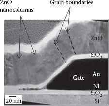
FIGURE 54.2 Cross-sectional TEM image of a ZnO film over the gate metal showing continuous, closely packed nanocolumnar structures over nonplanar surfaces. (B. Bayraktaroglu and K. Leedy, 2011 11th IEEE International Conference on Nanotechnology, August 15–18, Portland, Oregon, pp. 1450–1455. © (2011) IEEE. With permission.)
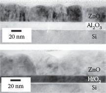
FIGURE 54.3 Cross-sectional TEM images of a ZnO thin film deposited at 200°C on Al2O3/Si and HfO2/Si. (B. Bayraktaroglu and K. Leedy, 2011 11th IEEE International Conference on Nanotechnology, August 15–18, Portland, Oregon, pp. 1450–1455. © (2011) IEEE. With permission.)
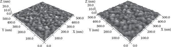
FIGURE 54.4 AFM images of ZnO thin films deposited at 200°C on (a) 20 nm SiO2/Si and (b) 30 nm HfO2/Si. (B. Bayraktaroglu and K. Leedy, 2011 11th IEEE International Conference on Nanotechnology, August 15–18, Portland, Oregon, pp. 1450–1455. © (2011) IEEE. With permission.)
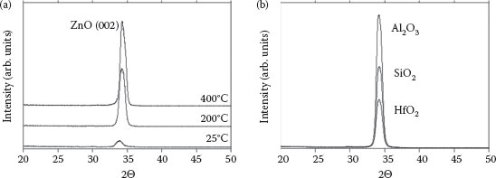
FIGURE 54.5 X-ray diffraction patterns of (a) ZnO thin films deposited on SiO2/Si at 25°C, 200°C, and 400°C and (b) ZnO thin films deposited at 200°C on SiO2/Si, Al2O3/Si, and HfO2/Si.
A summary of the TEM, SEM, and AFM characteristics of films grown at different temperatures is shown in Figure 54.6. Within the temperature range studied, the surface morphologies for all ZnO films showed no trend in grain size with deposition temperature. AFM images with the 500 nm × 500 nm collection areas in this figure also show that the films were predominantly smooth.
RMS roughness values ranged from 0.65 to 1.65 nm. Although the lowest roughness occurred in a film deposited at 200°C, no trend in roughness as a function of deposition temperature was observed. The RMS roughness is similar to other reported values of ZnO deposited by PLD [11,12]. Grain size calculations based on grain boundary intercepts in a scanning probe image processing software indicated 25–35 nm ZnO grains, again with no trend observed as a function of deposition temperature.
The typical common-source I–V characteristics of nc-ZnO TFTs fabricated on the HfO2, SiO2, and Al2O3 gate insulators are shown in Figure 54.7. The ZnO films were grown at 200°C and the devices were fabricated in the same fabrication batch for a direct comparison of results. All devices showed hysteresis-free operation and positive threshold voltages of 1.5 ± 0.6 V. As expected, higher dielectric constants of Al2O3 and HfO2 compared to SiO2 resulted in higher drain currents for the same gate voltage (i.e., higher transconductance) and flatter current characteristics in the saturation region.
The influence of the gate insulator on the device transconductance is shown in Figure 54.8. The same reciprocal dependence of transconductance on the gate length was obtained for these insulators in the gate length range of LG = 2–25 µm. This indicates that the number of charge states at the insulator–ZnO interface is low and such charges do not heavily influence the device operation.
The low interface state density values can also be inferred from the near-ideal subthreshold voltage swing, S, values typically obtained with the nc-ZnO TFTs. From the transfer characteristics shown in Figure 54.9, we determine the S-values of 74 and 107 mV/decade for devices with the SiO2 and HfO2 gate insulators. These S-values correspond to the total surface state density values of 2.51 × 10¹¹ and 5.38 × 1012 cm−2 using the expression developed in Ref. [15]. These transfer characteristics also show very high on/off ratios of about 1012, which is typical for the nc-ZnO TFTs fabricated on other substrates [16]. The maximum field-effect mobility for the nc-ZnO TFT with HfO2 gate insulators was 63 cm2/V · s, as shown in Figure 54.10. Field-effect mobility values of as high as 110 cm2/V · s were obtained with SiO2 gate insulator devices due to exceptionally low interface state densities [16,17].
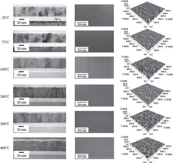
FIGURE 54.6 Cross-sectional TEM images, surface SEM images, and AFM images of ZnO thin film deposited on 20 nm SiO2/Si at 25°C, 75°C, 100°C, 200°C, 300°C, and 400°C.
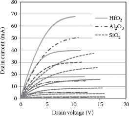
FIGURE 54.7 I–V characteristics of nc-ZnO TFTs with various gate insulators. Gate insulator thickness = 30 nm, LG = 5 µm, WG = 400 µm, VG = 2 V/step. (B. Bayraktaroglu and K. Leedy, 2011 11th IEEE International Conference on Nanotechnology, August 15–18, Portland, Oregon, pp. 1450–1455. © (2011) IEEE. With permission.)
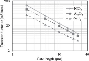
FIGURE 54.8 Transconductance dependence on gate length for three different gate insulators. VD = 12 V, VG = 10 V. (B. Bayraktaroglu and K. Leedy, 2011 11th IEEE International Conference on Nanotechnology, August 15–18, Portland, Oregon, pp. 1450–1455. © (2011) IEEE. With permission.)
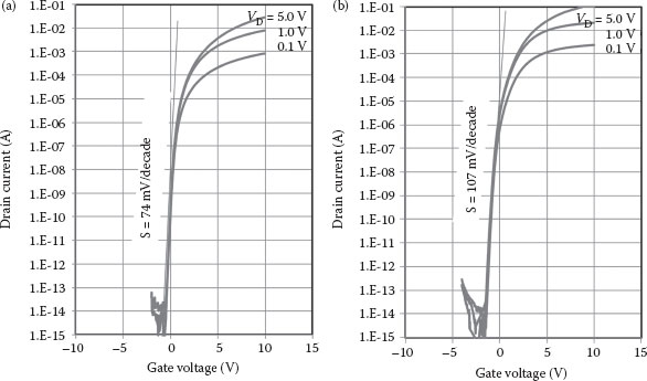
FIGURE 54.9 Transfer characteristics of nc-ZnO TFTs with (a) SiO2 and (b) HfO2 gate insulators for various drain voltage values. ZnO films were grown at 200°C. LG = 2 µm, and WG = 400 µm.
We interpret these record performance values for nc-ZnO TFTs deposited in O2 to be a result of high crystal quality preserved within nanocolumns as well as the presence of acceptor-like charges at the grain boundaries due to Zn-vacancies [9]. Transistors show exceptionally low leakage currents in the OFF state due to back-to-back depletion layers formed at the vertical grain boundaries, which effectively block horizontal current conduction between the source and the drain contacts.
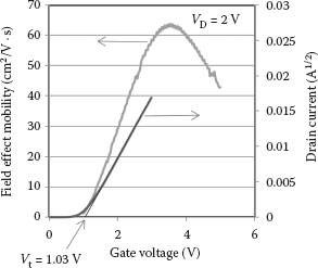
FIGURE 54.10 Field-effect electron mobility and drain current as a function of gate voltage for an nc-ZnO TFT fabricated on a polyimide substrate at low temperatures. LG = 5 µm, WG = 400 µm. (B. Bayraktaroglu and K. Leedy, 2011 11th IEEE International Conference on Nanotechnology, August 15–18, Portland, Oregon, pp. 1450–1455. © (2011) IEEE. With permission.)
In the ON state, the vertical depletion layers collapse under the influence of the gate field and large current densities are made possible between nanocrystals. This is similar to high current conduction in microcrystalline ZnO-based varistors where back-to-back depletion layers at grain boundaries rapidly collapse at high electric fields [18]. A combination of low leakage current in the OFF state and large current density in the ON state produces the very high ON/OFF ratios observed.
Other factors contributing to large current density operation are the high electron mobility and low interface state density described earlier. Such low interface state densities are consistent with the measured high field-effect mobility.
TFTs are mostly used in circuits that do not require high-speed operation [1] because of electron mobility limitations. However, with the demonstrated high electron mobility and the anticipated high electron velocity [19], ZnO-based TFTs have a greater potential for high-speed circuit applications than amorphous TFTs. Recently, devices capable of small-signal amplification at microwave frequencies were demonstrated using relatively long gate lengths of 1.2–3 µm [8,20].
In the design of high-speed transistors, several parasitic device elements must be minimized in addition to shrinking the gate length. The most prominent parasitic elements that degrade the high-frequency operation of a TFT are the gate resistance and the capacitance between the gate and the source/drain contacts. The location of the parasitic capacitances is illustrated in Figure 54.11.
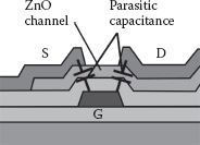
FIGURE 54.11 The parasitic capacitance between the source/drain and gate contacts that limit the high-frequency performance of the bottom-gate-type thin film transistors.
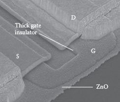
FIGURE 54.12 SEM picture showing the use of a thick gate insulator to reduce parasitic capacitance in high-speed TFTs.
The gate resistance can be lowered by the use of thick, high-conductivity metals such as Au or Cu. As shown in the cross-sectional drawing of Figure 54.2, a thick gate metal produces nonplanar topography for the bottom-gate-type transistors. It is important that the gate insulator and the ZnO thin film are produced conformably over the gate contact.
The parasitic capacitance resulting from the overlap of source/drain contacts over the gate can be reduced in several ways. The first is to minimize the overlap by careful alignment of these contacts and reduction of the actual gate length to as close to the source–drain spacing as possible (i.e., self-aligned contacts). The second is to employ a thicker gate insulator in the regions where the contacts overlap and a thinner gate insulator under the actual channel region. This approach requires the use of two different thickness gate insulators over the gate contact, as shown in Figure 54.12. Again, such an approach results in nonplanar surfaces over which the ZnO thin film is produced. However, the nc-ZnO films fabricated by PLD have shown that such topological variations can be readily overcome.
The high-speed potential of nc-ZnO TFTs was examined in a series of designs fabricated on high-resistivity Si substrates (>2000 ohm.cm). The gate contact was Ni/Au (5 nm/120 nm) to ensure low gate resistance. The gate insulator was PECVD SiO2 and the ZnO films were grown at 400°C. Devices with two different gate lengths (LG = 1.2 and 2.1 µm) and two different gate widths (WG = 50 and 100 µm) were used to examine device scalability. From the measured s-parameters, the maximum available gain (MAG) and current gain (|h21|2) values were determined as shown in Figure 54.13. The current gain |h21|2 values for both devices showed −6 dB/octave slopes with cut-off frequencies, fT, of 2.45 and 1.1 GHz for devices with LG = 1.2 and 2.1 µm, respectively. MAG values had slopes of −3 dB/octave for stability factor K < 1, and −6 dB/octave for K > 1. Power gain cut-off frequencies, fmax, of 7.45 and 3.02 GHz were achieved for the two size devices.
The cut-off frequency dependence on device size and bias conditions is shown in Figure 54.14. It is clear that the small-signal microwave performances of both size devices (i.e., WG = 50 and 100 µm) at the same bias conditions are nearly identical. This is an indication of good device scalability and indicates that the microwave performance is not degraded due to the increased gate resistance of longer gate fingers on larger devices. It also shows that the microwave performance has a weak dependence on gate bias and therefore on drain current. Such device characteristics, which are desirable for linear circuit applications, can be attributed to fully depleted channels characteristic of nc-ZnO TFTs.
Reduced parasitic capacitance with the use of double gate insulator thicknesses resulted in overall improvement in the high-speed performance of devices, as shown in Figure 54.15. Device designs with varying degrees of overlap between the source/drain contacts and the gate contact were examined for devices with LG = 1.2 µm and WG = 2 × 50 µm. All three device designs (with 1.5, 1.0, and 0.5 µm of gate electrode overlap with source/drain contacts) showed an identical current gain cut-off frequency of 2.9 GHz. The highest power cut-off frequency was fmax = 10 GHz for devices with a 0.5 µm overlap. To our knowledge, this is the highest-frequency operation obtained with any TFT using any material technology. Based on the small-signal device models extracted from the measured s-parameters, we expect fmax > 40 GHz for devices with LG = 0.5 µm.
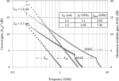
FIGURE 54.13 Small-signal microwave characteristics of ZnO TFTs with different gate lengths. The gate width was 100 µm for both devices.
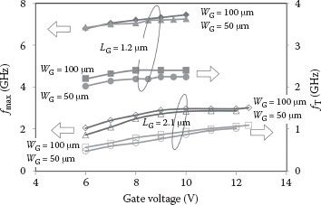
FIGURE 54.14 Microwave performance dependence on device size and gate voltage. Bias conditions were VD = 13 V for the LG = 1.2 µm device and VD = 16 V for the LG = 2.1 µm device.
54.4.3 TRANSPARENT TRANSISTORS
ZnO thin films are suitable for transparent thin film transistor (TTFT) applications because the wide bandgap properties (3.4 eV) of both doped and undoped layers can provide excellent optical transparency. The semiconducting properties of undoped layers make them suitable for active layers, as shown earlier, while the doped films can be considered for contact layers. An all-ZnO approach is important for this application because of the high cost and the worldwide shortage of indium caused by the rapidly increasing use of ubiquitous touch screen devices with ITO (indiumtin oxide) transparent conductive oxide (TCO) films [21].
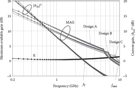
FIGURE 54.15 Small-signal microwave characteristics of nc-ZnO TFTs. TFTs with different gate contacts overlap with S/D contacts. Devices were biased at VG = 6 V, VD = 11 V. (B. Bayraktaroglu and K. Leedy, 2011 11th IEEE International Conference on Nanotechnology, August 15–18, Portland, Oregon, pp. 1450–1455. © (2011) IEEE. With permission.)
The resistivity, transparency, and stability of contact layers made of Al- or Ga-doped ZnO films were shown to be competitive with indium-based TCOs [22, 23, 24 and 25]. However, the integration of doped and undoped ZnO films in the same device faces some technical challenges, including low-temperature processing for contact layers, autodoping between layers, and the lack of selective etching between doped and undoped ZnO films.
We have developed indium-free transparent transistors by replacing the metal contacts of the nontransparent TFTs described earlier with Ga-doped ZnO films grown at low temperatures and in an Ar atmosphere [26]. These Ar-grown TCOs do not require postgrowth annealing to achieve low resistivity and therefore comply with the low process temperature budget of ≤200°C. To address the difficulty of selectively etching the contact layer over the channel (both ZnO), we employed a thin Ti etch-stop layer between the source/drain contacts and the transistor channel layer as shown in Figure 54.16. During processing, the exposed parts of this etch-stop layer oxidized and became a nonconducting TiOx surface passivation layer.
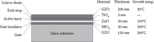
FIGURE 54.16 The entire thin film stack of indium-free TTFT grown on a transparent substrate at successively lower growth temperatures. (B. Bayraktaroglu and K. Leedy, 2011 11th IEEE International Conference on Nanotechnology, August 15–18, Portland, Oregon, pp. 1450–1455. © (2011) IEEE. With permission.)
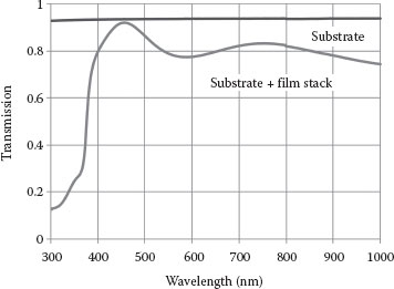
FIGURE 54.17 Optical transmission rate for the entire TTFT films and the glass substrate. (B. Bayraktaroglu and K. Leedy, 2011 11th IEEE International Conference on Nanotechnology, August 15–18, Portland, Oregon, pp. 1450–1455. © (2011) IEEE. With permission.)
The entire film stack was grown on glass or quartz substrates before device fabrication and had about 90% transparency (not including the substrate) in the visible spectrum, as shown in Figure 54.17. The growth temperature of layers was reduced as the layers were added to minimize the impact of temperature on the properties of the previously grown layers. The gate insulator was 30-nm-thick HfO2 grown by the ALD technique. Mesa etching techniques were used to define the S/D contacts, device active area, and gate contacts in successive process steps. Figure 54.18 shows a cross-sectional drawing of the transistor and a photograph of several devices with different gate lengths ranging from 5 to 20 µm.
The linear portion of the I–V characteristics of a device with LG = 5 µm and WG = 70 µm, shown in Figure 54.19, indicates that the GZO layers make good ohmic contacts with the active layer and there is no evidence of current blocking by the TiOx etch-stop layer. Also, devices exhibit excellent sauration characteristics for this gate length dimension. The current density was lower than the nontransparent devices fabricated on Si substrates due to the thermal limitations of the glass substrate.
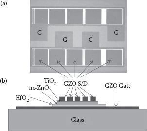
FIGURE 54.18 (a) A photograph and (b) a cross-sectional drawing of transparent nc-ZnO TFTs. A thin TiOx layer is employed as an etch-stop layer to facilitate the selective etching of S/D GZO layers. (B. Bayraktaroglu and K. Leedy, 2011 11th IEEE International Conference on Nanotechnology, August 15–18, Portland, Oregon, pp. 1450–1455. © (2011) IEEE. With permission.)
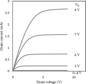
FIGURE 54.19 Current–voltage characteristics of the nc-ZnO TTFT. LG = 5 µm, WG = 70 µm, VG = 1 V/step. (B. Bayraktaroglu and K. Leedy, 2011 11th IEEE International Conference on Nanotechnology, August 15–18, Portland, Oregon, pp. 1450–1455. © (2011) IEEE. With permission.)
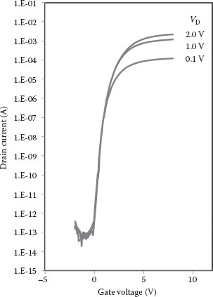
FIGURE 54.20 Transfer characteristics of the indium-free nc-ZnO TTFT. (B. Bayraktaroglu and K. Leedy, 2011 11th IEEE International Conference on Nanotechnology, August 15–18, Portland, Oregon, pp. 1450–1455. © (2011) IEEE. With permission.)
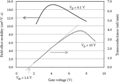
FIGURE 54.21 Field-effect mobility and transconductance of the indium-free nc-ZnO TTFT as a function of gate voltage. (B. Bayraktaroglu and K. Leedy, 2011 11th IEEE International Conference on Nanotechnology, August 15–18, Portland, Oregon, pp. 1450–1455. © (2011) IEEE. With permission.)
The transfer characteristics shown in Figure 54.20 exhibit an on/off ratio of 5 × 10¹⁰ and a subthreshold voltage swing of S < 200 mV/decade. These values are comparable to the values obtained with nontransparent devices fabricated within the same temperature budget.
The field-effect electron mobility and transconductance values obtained from the transfer characteristics are shown in Figure 54.21. The threshold voltage, Vth = 1.6 V, was slightly higher than the value obtained with nontransparent devices (i.e., Vth = 1.03 V). On the other hand, the maximum field-effect mobility, 15 cm2/V · s, was lower than the value obtained with nontransparent devices. The measured S value corresponds to an increase in the interface state density to 4.61 × 1012 cm−2, which can explain the corresponding decrease in mobility. A higher interface state density can be caused by the ZnO–HfO2 interface roughness [27] due to the rougher gate contact layer surfaces compared to the metal gates used in nontransparent devices. Improvements in the surface morphology of the doped nc-ZnO gate contact layer are expected to bring closer the performance metrics of the transparent and nontransparent transistors. Nevertheless, to our knowledge, the performance values reported here represent the highest values obtained with indium-free TTFTs.
PLD-grown ZnO thin films were used to fabricate high-speed and transparent thin film transistors. TEM and x-ray examination showed that films consisted of closely packed nanocolumns of ZnO with a predominantly (002) orientation and 20–50 nm diameter. Films maintained their ordered structure conformably over nonplanar surfaces. We have studied doped and undoped films grown on various gate insulators and at low substrate temperatures for high-speed and transparent thin film transistor applications. Excellent switching characteristics (on/off ratios greater than 1012), subthreshold voltage swing (S = 74 mV/decade), and field-effect mobilities (63 cm2/V · s) were obtained with low-temperature grown films. We attributed these superior performances of nc-ZnO TFTs to the high crystal quality preserved within nanocrystals and the presence of acceptor-like states at the vertical grain boundaries due to Zn-vacancies. High-speed performance was demonstrated by devices fabricated on Si substrates with the achievement of a current gain cut-off frequency of 2.9 GHz and a power gain cut-off frequency of 10 GHz. Doped and undoped nc-ZnO films were integrated on glass substrates using etch-stop layers to fabricate the first all-ZnO TTFTs with record performance. Indium-free TTFTs are important to address the cost and availability issues related to indium.
This work was supported in part by AFOSR under LRIR No. 07SN03COR (Program Manager: Dr. Jim Hwang). The authors thank D. Agresta, J. Brown, and D. Tomich for optical transmission, AFM, and XRD analyses, respectively.
1. C. R. Kagan and P. Andry,Thin Film Transistors, Marcel Dekker Publishing, New York, 2003.
2. K. Nomura, H. Ohta, A. Takagi, T. Kamiya, M. Hirano, and H. Hosono, Room temperature fabrication of transparent flexible thin-film transistors using amorphous oxide semiconductors,Nature, 432, 488–492, 2004.
3. T. Kamiya, K. Nomura and H. Hosono, Present status of amorphous In–Ga–Zn–O thin-film transistors, Sci. Technol. Adv. Mater., 11, 044305, 2010.
4. D. A. Mourey, D. A. Zhao, J. Sun, and T. N. Jackson, Fast PEALD ZnO thin-film transistor circuits, IEEE Trans. Elect. Dev., 57, 530–534, 2010.
5. H. Hosono, Ionic amorphous oxide semiconductors: Material design, carrier transport, and device application, J. Non-crystalline Solids, 352, 851–858, 2006.
6. D. Zhao, D. A. Mourey, and T. N. Jackson, Gamma-ray irradiation of ZnO thin film transistors and circuits, 2010 Device Research Conference Technical Digest, pp. 241–242, 2010.
7. B. Bayraktaroglu, K. Leedy, Y. V. Li, D. Zhao, I. Ramirez, H. H. Fok, and T. N. Jackson, Radiation tolerance and recovery characteristics of ZnO thin film transistors, GOMACTech-12 Conference Technical Digest, pp. 193–196, 2012.
8. B. Bayraktaroglu, K. Leedy, and R. Neidhard, Nanocrystalline ZnO microwave thin film transistors, Proc. SPIE, 7679, 767904–1, 2010.
9. R. C. Scott, K. Leedy, B. Bayraktaroglu, D. C. Look, and Y.-H. Zhang, Effects of Ar vs. O2 ambient on pulsed-laser-deposited Ga-doped ZnO, J. Cryst. Growth, 324, 110–114, 2011.
10. L. Bentes, R. Ayouchi, C. Santos, R. Schwarz, P. Sanguino, O. Conde, M. Peres, T. Monteiro, and O. Teodoro, ZnO films grown by laser ablation with and without oxygen CVD, Superlattices Microstruct., 42, 152–157, 2007.
11. S. Amirhaghi, V. Craciun, D. Craciun, J. Elders, and I. W. Boyd, Low temperature growth of highly transparent c-axis oriented ZnO thin films by pulsed laser deposition, Microelectron. Eng., 25, 321–326, 1994.
12. L. Han, F. Mei, C. Liu, C. Pedro, and E. Alves, Comparison of ZnO thin films grown by pulsed laser deposition on sapphire and Si substrates, Physica E, 40, 699–704, 2008.
13. C.-F. Yu, C.-W. Sung, S.-H. Chen, and S.-J. Sun, Relationship between the photoluminescence and conductivity of undoped ZnO thin films grown with various oxygen pressures, Appl. Surf. Sci., 256, 792–796, 2009.
14. B. Bayraktaroglu, K. Leedy, and R. Neidhard, ZnO thin film transistors for RF applications, Mater. Res. Soc. Symp. Proc., 1201, H09–07, 2010.
15. A. Roland, J. Richard, J. P. Kleider, and D. Mencaraglia, Electrical properties of amorphous silicon transistors and MIS-devices: Comparative study of top nitride and bottom nitride configurations, J. Electrochem. Soc., 140, 3679–3683, 1993.
16. B. Bayraktaroglu, K. Leedy, and R. Neidhard, Microwave ZnO thin-film transistors, IEEE Electron Dev. Lett., 29, 1024–1026, 2008.
17. S.-J. Chang, M. Bawedin, B. Bayraktaroglu, J.-H. Lee, S. Cristoloveanu, Low–temperature properties of ZnO on insulator MOSFETs, IEEE Int. SOI Conf., Tempe, AZ, 2011.
18. D. R. Clarke, Varistor Ceramics, J. Am. Ceram. Soc., 82, 485–502, 1999.
19. J. Albrecht, P. P. Ruden, S. Limpijumnong, W. R. Lambrecht and K. F. Brennan, High field electron transport properties of bulk ZnO, J. Appl. Phys., 86, 6864–6867, 1999.
20. B. Bayraktaroglu, K. Leedy, and R. Neidhard, High-frequency ZnO thin film transistors on Si substrates, IEEE Electron Dev. Lett., 30, 946–948, 2009.
21. B. O’Neill, Indium market forces, a commercial perspective, 35th IEEE Photovoltaic Specialists Conference (PVSC) Proceedings, DOI: 10.1109/PVSC.2010.5616842, 2010.
22. H. Agura, A. Suzuki, T. Matsushita, T. Aoki, and M. Okuda, Low resistivity transparent conducting Al-doped ZnO films prepared by pulsed laser deposition, Thin Solid Films, 445, 263–267, 2003.
23. B. Bayraktaroglu, K. Leedy and R. Bedford, High temperature stability of postgrowth annealed transparent and conductive ZnO:Al films, Appl. Phys. Lett., 93, 022104, 2008.
24. T. Minami, S. Ida, and T. Miyata, High rate deposition of transparent conducting oxide thin films by vacuum arc plasma evaporation, Thin Solid Films, 416, 92–96, 2002.
25. R. C. Scott, K. Leedy, B. Bayraktaroglu, D. Look, D. Smith, D. Ding, X. Lu, and Y.-H. Zhang, Influence of substrate temperature and post-deposition annealing on material properties of Ga-doped ZnO prepared by pulsed laser deposition, J. Electronic Mat., 40, 419–428, 2010.
26. R. C. Scott, K. Leedy, B. Bayraktaroglu, D. Look, and Y.-H. Zhang, Highly conductive ZnO grown by pulsed laser deposition in pure Ar, Appl. Phys. Lett., 97, 072113, 2010.
27. K. Okamura and H. Hahn, Carrier transport in nanocrystalline field-effect transistors: Impact of interface roughness and geometrical carrier trap, Appl. Phys. Lett., 97, 153114, 2010.
28. B. Bayraktaroglu and K. Leedy, Ordered nanocrystalline ZnO films for high speed and transparent thin film transistors, 2011 11th IEEE International Conference on Nanotechnology, August 15–18, Portland, Oregon, pp. 1450–1455.