![Chapter 55 First-Principle Study of Energy-Band Control by Cross-Sectional Morphology in [110]-Si Nanowires](https://imgdetail.ebookreading.net/cover/cover/system_admin/EB9781466565241.jpg)
First-Principle Study of Energy-Band Control by Cross-Sectional Morphology in [110]-Si Nanowires |
CONTENTS
55.3.1 Effects of Cross-Sectional Shape
55.3.2 Origins of Dependence on Cross-Sectional Shapes
55.3.3 Effects of Sidewall Roughness
Si nanowire field-effect transistors (SiNW FETs) are expected to be boosters in postscaling semiconductor technology. Bangsaruntip et al. have indeed achieved excellent control of SiNW sizes utilizing conventional complementary metal oxide semiconductor (CMOS) fabrication processes and then observed clear scaling of short-channel effects versus NW sizes with the fixed gate length [1]. Reducing the dimensions of SiNWs is shown to improve the short-channel control. They have fabricated the [110]-SiNW FETs with channel dimensions of 5.0 nm × 6.3 nm and even smaller, 2.0 nm × 3.3 nm. In such small dimensions, quantum confinement becomes prominent. In addition, SiNW FETs with various sizes and shapes, including circular, elliptic, and rectangular, have been fabricated [2, 3, 4, 5 and 6]. The quantum effects depend on crystallographic directions of the SiNW axes and also on the cross-sectional morphology of the SiNWs, resulting in substantial modification of the energy-band structures and the transport characteristics of SiNW FETs.
Hydrogenated SiNWs that are formed by treatments of pristine or oxidized SiNWs with hydrogen fluorides offer a stage where salient properties of SiNWs are investigated. Electronic structures of such hydrogenated SiNWs have been indeed studied by density functional theory (DFT) [7, 8, 9, 10, 11, 12 and 13], although the NWs considered so far are much thinner than those experimentally synthesized. Ng et al. and Leu et al. have investigated band structures of SiNWs oriented along the [100], [110], [111], and [112] directions and shown variation of the bandgaps as a function of the diameter [9,10]. Ng et al. have further explored the effects of cross-sectional shapes on bandgaps in [110]-SiNWs with a diameter of about 1 nm and argued that the effects are minor [9]. Other DFT calculations provide different results, however. Singh et al. and Sorokin et al. have found that energy-band structures of hydrogenated SiNWs with diameters less than 2.0 nm depend strongly on the cross-sectional morphology [11,12]. Even though the SiNWs are oriented along the same direction and the dimensions of the wires are close to each other, they have direct or indirect gaps depending on the morphology. Hence, at the present stage, the relation between the cross-sectional morphology and the electronic structure is under debate even in thin NWs. The relation in the thicker SiNWs experimentally available has not been discussed in the past. Clarifying the underlying physics that is decisive to determine the electronic structure is in high demand.
Furthermore, Scheel et al. have calculated the density of states (DOS) of [110]-SiNW [13], and found that the conduction-band minimum (CBM) at the zone center Γ contributes only small DOS, whereas the second minimum that is located at some point between the Γ and the zone boundary X provides a peak of DOS peculiar to a one-dimensional system. This aspect is extremely important to discuss the characteristics of SiNW FETs.
Hence, it is imperative to clarify the electronic structures of SiNWs, focusing not only on the bandgap but also on the relative locations of several energy minima and its morphology dependence. We have performed extensive electronic structure calculations based on the DFT for [110]-and [100]-SiNWs with various cross-sectional shapes.
On the other hand, sidewalls of the SiNWs calculated by the earlier-cited papers are of ideal structures without roughness, namely, there are few calculations based on DFT about a local cross-sectional morphology. In the experiment, however, SiNWs have subnanometer roughness by oxidation or etching in fabrication processes [1]. Therefore, we have also investigated the effects of sidewall roughness by changing amounts of the roughness and a pattern of the roughness.
We have found that [110]-SINWs have lighter electron effective masses compared to [100]-SiNWs. In this chapter, restricting ourselves to the [110]-SiNWs, we report on DFT calculations that clarify the relationship between structural morphology and energy bands.
Calculations have been performed in the local density approximation (LDA) in DFT [14,15]. Normconserving pseudopotentials generated by using the Troullier–Martins scheme are adopted to describe the electron–ion interaction [16,17]. We use our newly developed real-space finite-difference scheme [18] that allows us to perform LDA calculations for systems with tens of thousands of atoms on a few tens-of-Tera FLOPS computers. The grid spacing in the real-space calculations is taken to be 0.034 nm, corresponding to the cutoff energy of 260 eV, which is calculated by
(55.1) |
where d is the grid spacing in real space. The sixth-order finite difference is adopted for the kinetic energy operator. We use a supercell model in which [110]-SiNWs are arranged periodically. To avoid interactions among the SiNWs, they are separated from each other by at least 10+. We take five k points along the [110] direction in the Brillouin zone (BZ) integration. These calculational parameters assure the accuracy required in this work. Sidewalls of the wires are terminated by hydrogen atoms, reflecting certain experimental situations on the one hand and focusing on essential features of the energy bands on the other. The starting geometry for each SiNW is constructed by cleaving the bulk Si. Geometry optimization has been performed until the maximum force becomes less than 0.5 eV/nm.
The sidewall roughness of SiNWs is introduced as a random fluctuation of the radius of the nanowire around an average radius. In cylindrical coordinates, the radius of the rough wire is expressed as follows:
(55.2) |
where R0 is the average radius. The distribution of the random fluctuation is characterized by assuming the following autocorrelation function [19,20]:
(55.3) |
where Δm is the root mean square of the radius fluctuation and Lm is the correlation length. In our calculation, we examined four values from 0.2 to 0.8 nm, which seem to be realistic. In addition, we examined three-pattern SiNWs with sidewall roughness in 0.4 nm of the root mean square. We set 0.54 and 4.3 nm for Lm and R0, respectively.
55.3.1 EFFECTS OF CROSS-SECTIONAL SHAPE
We have explored various [110]-SiNWs with the dimensions ranging from 3 to 6 nm. Figure 55.1 shows some examples of cross-sectional views of obtained geometry-optimized [110]-SiNWs, representing typical cross-sectional shapes. The dimensions of these wires are close to each other as shown. Both Figure 55.1b and d show the elliptic cross-sectional shapes, but their extended directions are not equivalent to each other. We call the ellipses that have the long axes along the [001] and the directions and the [001]-ellipse and the -ellipse, respectively. Similarly, the dumbbells that are shown in Figure 55.1c and e are called the [001]-dumbbell and -dumbbell.
Figure 55.2 shows the calculated conduction-band structure near the gap for each SiNW shown in Figure 55.1. These band structures qualitatively agree with the results in the past for the thinner [110]-SiNWs [9,12,13]. Table 55.1 shows the calculated bandgaps and effective masses. In all cases, the conduction-band minima are located at the zone center Γ, whereas the second minima are located at approximately 85% from the Γ to the X, which we call Δ0. The energy at each minimum is shifted from the bulk conduction-band bottom by Eshift due to the quantum confinement. In Figure 55.2, the difference ΔEshift between the first and the second minima is also shown. The Γ-point minimum originates from the two valleys along [00 ± 1] of the conduction bands in bulk Si, whereas the second minimum comes from another two valleys along the [010] and the [100] directions, respectively. Hence, all the minima are doubly degenerate.
This situation is clearly recognized in Figure 55.3. In the plane perpendicular to the [110] direction, two primitive vectors, a1 and a2, are introduced. Together with the primitive vector along the [110] direction, a unit cell is defined and the corresponding BZ is shown in Figure 55.3b. The six conduction-band valleys in an original BZ corresponding to the diamond structure are shown in this new BZ. The [00 ± 1] valleys are marked in dark gray, whereas the [±100] and [0 ± 10] are marked in light gray. In Figure 55.3c and d, we show the energy contours of the conduction band near the valleys on the planes perpendicular to the wire axis. We indeed observe the corresponding conduction-band valleys on these contour lines. The energy bands become minimum at the wave number projected on the [110] direction of each valley, thus leading to the behavior shown in Figure 55.2.
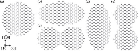
FIGURE 55.1 Cross-sectional views of various [110]-SiNWs. Large and small balls represent Si and H atoms, respectively: (a) the circle whose diameter is 4.3 nm, (b) the [001]-ellipse, (c) the [001]-dumbbell, (d) the -ellipse, and (e) the -dumbbell. (S. Kyogoku et al., First-principle study of energy-band control by cross-sectional morphology in [110]-Si nanowires. 2011 11th IEEE Conference on Nanotechnology (IEEE-NANO), Portland, OR, pp. 1322–1326, © (2011) IEEE. With permission.)
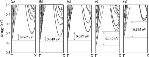
FIGURE 55.2 Conduction-band structures of various SiNWs shown in Figure 55.1: (a) the circle, (b) the [001]-ellipse, (c) the [001]-dumbbell, (d) the -ellipse, and (e) the -dumbbell. The values of ΔEshift are also shown. The origin of the energy is at the valence-band top. The bandgap of the bulk Si is 0.49 eV in the present LDA calculations. (S. Kyogoku et al., First-principle study of energy-band control by cross-sectional morphology in [110]-Si nanowires. 2011 11th IEEE Conference on Nanotechnology (IEEE-NANO), Portland, OR, pp. 1322–1326, © (2011) IEEE. With permission.)
TABLE 55.1
Calculated Bandgap in Increases and Effective Masses of [110] SiNWs
Bandgap (eV) |
|||
Circle |
0.633 |
0.16 |
0.60 |
[001]-dumbbell |
0.621 |
0.15 |
0.63 |
[001]-ellipse |
0.632 |
0.14 |
0.61 |
-ellipse |
0.578 |
0.15 |
0.63 |
-dumbbell |
0.666 |
0.17 |
0.59 |
Our results clearly show that the bandgap, the effective mass, and the ΔEshift depend on the cross-sectional shapes. The bandgap of the -ellipse is the narrowest, and that of the -dumbbell is the widest among all the cross-sectional shapes considered here. The difference between the two is 88 meV. All the effective masses at Γ, m*Γ, are smaller than the transverse (lighter) mass of the Si bulk, mt = 0.19. This modification of the effective mass from the bulk value can be explained in terms of the nonparabolicity and anisotropy near the conduction-band valleys of Si [21].
The effective mass at Δ0, m*Δ0, is between the longitudinal mass ml (=0.95) and mt for any cross-sectional shaped SiNW. This finding is a consequence of the wire-axis direction being obliquely crossed with the longitudinal direction of the conduction-band valleys along [100] and [010] as shown in Figure 55.3b.
As for the ΔEshift, the [001]-ellipse and the dumbbell provide smaller values than the -ellipse and the dumbbell. In addition, the ΔEshift of the [001]-ellipse is smaller than that of the circle. Energy shifts of the dumbbell-shaped NWs are larger than those of the elliptic-shaped NWs, irrespective of the extended direction. This is attributed to the fact that the standing waves in the perpendicular plane in the dumbbell-shaped NWs have the maximum amplitude at two points even for the lowestenergy state. Our results unequivocally show that the [001]-ellipse SiNW has benefits in terms of the number of channels under the ballistic regime of FETs. The difference between the largest and the smallest ΔEshift is 116 meV, which is larger than the difference of the bandgap, indicative of the importance of cross-sectional morphology in the characteristics of NW-FETs.
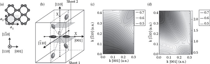
FIGURE 55.3 (a) Two primitive vectors a1 and a2 in the plane perpendicular to the wire-axis direction; (b) corresponding first Brillouin zone and the six conduction-band valleys. The planes named by sheet 1 and sheet 2 cut across the center of each conduction-band valley. Energy contour plots on the planes named by sheet 1 and sheet 2 are shown in (c) and (d), respectively, in eV units. (S. Kyogoku et al., First-principle study of energy-band control by cross-sectional morphology in [110]-Si nanowires. 2011 11th IEEE Conference on Nanotechnology (IEEE-NANO), Portland, OR, pp. 1322–1326, © (2011) IEEE. With permission.)
55.3.2 ORIGINS OF DEPENDENCE ON CROSS-SECTIONAL SHAPES
Our findings explained above come from the fact that the wave numbers in the plane perpendicular to the wire axis become discrete, depending on the cross-sectional shapes, and that the energy minima along the wire axis at these discrete wave numbers are different from each other. To elucidate this point, we consider an SiNW that has a rectangular cross section with dimensions of L1 = n1a1| × L2 = n2|a2|.
Then the wave numbers in the first BZ allowed in the perpendicular plane become
(55.4) |
To mimic the circle- and the ellipse-shaped NWs examined earlier, we consider the three-type rectangular SiNWs: (1) a rectangular shape extended along , (2) a nearly square shape, and (3) a rectangular shape extended along [001]. We call them the -rectangular, the square, and the [001]-rectangular, respectively. Figure 55.4 shows the allowed wave numbers on the perpendicular plane for the three rectangular-shaped NWs introduced earlier. Some of the energy contours shown by thick lines in Figure 55.3c and d are reproduced in Figure 55.4.
In the -rectangular NW (Figure 55.4a), the confinement along the [001] direction is stronger than that along the direction. Hence, the discrete wave numbers are sparsely distributed along the [001] direction compared with the direction. Consequently, the allowed wave vector marked by the square is close to CBM in the [00 ± 1] valley, whereas the allowed wave vector marked by the circle is less close to the CBM in the [100] and [010] valleys. The former corresponds to the Γ-point minimum and the latter to the Δ0-point minimum in the dispersion along [110]. Therefore, we obtain relatively large ΔEshift in this case.
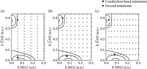
FIGURE 55.4 Allowed wave numbers on the plane perpendicular to the [110] wire axes for the three rectangular NWs. The side lengths of the three rectangular NWs are (a) 5.3 nm × 3.2 nm, (b) 3.8 nm × 4.3 nm, and (c) 2.3 nm × 7.0 nm. Gray diamonds and black squares and circles show the allowed wave numbers. Energy contours near the conduction-band minima shown by thick lines in Figure 55.3c and d are also shown. The allowed wave numbers that are the closest to the conduction-band minimum along [001] and along are marked by a black square and a black circle, respectively. Values of k are in units of the corresponding BZ. (S. Kyogoku et al., First-principle study of energy-band control by cross-sectional morphology in [110]-Si nanowires. 2011 11th IEEE Conference on Nanotechnology (IEEE-NANO), Portland, OR, pp. 1322–1326, © (2011) IEEE. With permission.)
On the contrary, in the [001]-rectangular NW (Figure 55.4c), the confinement along the direction is stronger than that along the [001] direction. Hence, the discrete wave numbers are densely distributed along the [001] direction compared with the direction. Consequently, the allowed wave vector marked by the square is far from CBM in the [00 ± 1] valley, whereas the allowed wave vector marked by the circle is close to the CBM in the [100] and [010] valleys. Therefore, we obtain relatively small ΔEshift in this case.
These results obtained in the rectangular-shaped NW models are consistent with the calculated ΔEshift for real SiNWs shown in Figure 55.2. We thus argue that the cross-sectional shape is an important factor in determining ΔEshift and the properties of SiNW FETs.
55.3.3 EFFECTS OF SIDEWALL ROUGHNESS
We showed the results of ideal-shaped NWs explained in Section 55.3.1. In the experiment, however, SiNWs have a subnanometer roughness by the oxidation or etching in fabrication processes [1], and it is difficult to eliminate roughness in the sidewall of SiNWs in their fabrication processes. Therefore, it is important to clarify the effects of sidewall roughness. These effects can be regarded as the effects of the cross-sectional morphology. If we call the effects explained in Section 55.3.1 as the global-shape effects, we can call these effects by the sidewall roughness effects as the local-shape effects.
To clarify these effects of sidewall roughness on DOS, we have explored [110]-SiNWs with sidewall roughness. The roughness is introduced as a radius fluctuation ranging from 0.2 to 0.8 nm. To examine the pure effects of the amounts of roughness, we calculate these SiNWs with sidewall roughness generated by a single set of random numbers in Equation 55.3. Figure 55.5 shows the cross-sectional views and side views from [111] of various [110]-SiNWs with sidewall roughness. All the averaged diameters are 4.3 nm. Moreover, to examine the effects of a roughness pattern, we calculate other two-pattern rough SiNWs that are generated by different sets of random numbers in Equation 55.3. Figure 55.6 shows the cross-sectional views and side views from [111] of such [110]-SiNWs with sidewall roughness. Indeed, these cross-sectional shapes are different from those shown in Figure 55.5b. All the averaged diameters are also 4.3 nm and the root mean squares of the radius fluctuations, Δm, are 0.4 nm in this case. As in Section 55.3.1, we have focused not only on the bandgap itself but also on the relative locations of several energy minima and DOS near the CBM.
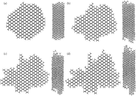
FIGURE 55.5 Cross-sectional views and side views from [111] of various [110]-SiNWs with sidewall roughness. The root mean squares of the radius fluctuation, Δm, are (a) 0.2 nm, (b) 0.4 nm (pattern 1), (c) 0.6 nm, and (d) 0.8 nm.
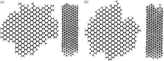
FIGURE 55.6 Cross-sectional views and side views from [111] of two-pattern rough SiNWs. The root mean square of the radius fluctuation, Δm, is 0.4 nm. (a) Pattern 2 and (b) pattern 3.
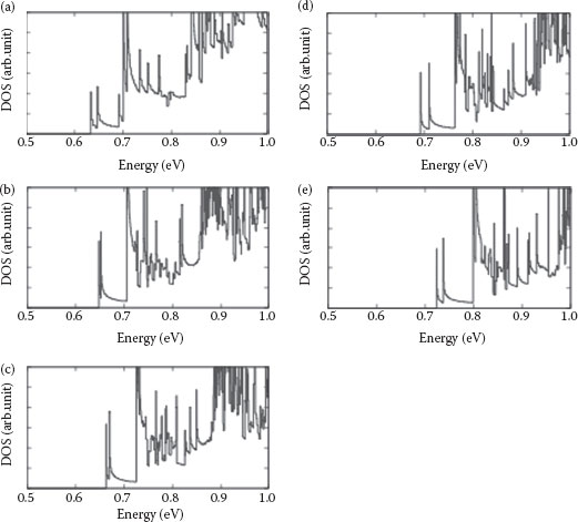
FIGURE 55.7 Densities of states with Δm of (a) 0.0 nm, which is shown in Figure 55.1a, (b) 0.2 nm, (c) 0.4 nm, (d) 0.6 nm, and (e) 0.8 nm.
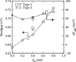
FIGURE 55.8 The bandgap and ΔEshift versus the amounts of roughness. The values of three patterns of roughness in 0.4 nm are also shown.
Figure 55.7 shows DOS of the SiNWs with sidewall roughness, along with the ideal SiNWs. Shapes of the DOS show a little change with or without the roughness. In addition, this tendency does not change by the amount of roughness. However, the energy shift of each peak increases with an increase in the roughness. Figure 55.8 shows variations of a bandgap and a ΔEshift of SiNWs with sidewall roughness. We found that the bandgap increases with an increase in the amount of roughness. This is attributed to the fact that the wave function confinement is narrower than that in those ideal structures due to sidewall roughness. In contrast, there is little change in the ΔEshift versus the amount of roughness. This indicates that the ΔEshift is unaffected by change of a local cross-sectional shape near the sidewall. According to the results of pattern 2 and pattern 3 in 0.4 nm of the root mean fluctuation, we can find that these behaviors are unchanged by the pattern of sidewall roughness. The reason why ΔEshift is unchanged is given by the discussion in Section 55.3.2. The allowed discrete wave numbers only depend on the global cross-sectional shapes of the SiNWs. Hence, ΔEshift does not depend on the local cross-sectional shape of the SiNWs.
We have performed extensive electronic structure calculations based on the LDA in DFT for [110]-SiNWs with various cross-sectional shapes with the diameter ranging from 3 to 6 nm. We have found that the quantum effects substantially modify the energy bands, and that the global cross-sectional shapes play important roles in the modification. We have found that the [110]-SiNWs with the elliptic cross section extending in the [001] direction has the largest number of channels within 50 meV from the conduction-band bottom, thus being a good candidate for FET applications.
We have analyzed our LDA results by using simple rectangular-shaped NW structures, and found that the substantial effects of the cross-sectional morphology come from the particular arrangement of the allowed wave numbers in the lateral BZ, and that the particular arrangement is peculiar to each cross-sectional shape. The relative positions of the allowed wave numbers to the conduction-band bottom are crucial in determining the number of channels. Moreover, we have performed the DOS of SiNWs with sidewall roughness with an average diameter of 4.3 nm. We have found that sidewall roughness does not modify the shape of DOS, but increases the energy shift. Therefore, the bandgap increases as the amounts of roughness increase. However, we have found that the relative locations of several energy minima near the CBM do not depend on the amounts and the pattern of sidewall roughness. In conclusion, we have clarified the significance of the global-shape effects and the insignificance of the local-shape effects that imply the sidewall roughness for the number of channels near the CBM. The knowledge obtained here is applicable to other crystallographic directions, opening a possibility to the design and fabrication of optimum SiNWs for FETs.
1. S. Bangsaruntip, G. M. Cohen, A. Majumdar, Y. Zhang, S. U. Engelmann, N. C. M. Fuller, L. M. Gignac et al., High performance and highly uniform gate-all-around silicon nanowire MOSFETs with wire size dependent scaling, in IEDM Tech. Dig., 297, 2009.
2. S. D. Suk, K. H. Yeo, K. H. Cho, M. Li, Y. Y. Yeoh, K.-H. Hong, S.-H. Kim et al., Investigation of nanowire size dependency on TSNWFET, in IEDM Tech. Dig., 717, 2005.
3. K. H. Yeo, S. D. Suk, M. Li, Y. Y. Yeoh, K. H. Cho, K.-H. Hong, S.-K. Yun et al., Gate-all-around (GAA) twin silicon nanowire MOSFET (TSNWFET) with 15 nm length gate and 4 nm radius nanowires, in IEDM Tech. Dig., 539, 2006.
4. M. Li, K. H. Yeo, S. D. Suk, Y. Y. Yeoh, D.-W. Kim, T. Y. Chung, K. S. Oh, and W.-S. Lee, Sub-10 nm gate-all-around CMOS nanowire transistors on bulk Si substrate, in VLSI Tech. Dig., 123, 2009.
5. H. S. Wong, L.-H. Tan, L. Chan, G.-Q. Lo, G. Samudra, and Y.-C. Yeo, Gate-all-around uantum-wire field-effect transistor with Dopant Segregation at Metal-Semiconductor-Metal heterostucture, in VLSI Tech. Dig., 92, 2009.
6. C. Dupré, A. Hubert, S. Becu, M. Jublot, V. Maffini-Alvaro, C. Vizioz, F. Aussenac et al., 15 nm-diameter 3D stacked nanowires with independent gates operation: ΦFET, in IEDM Tech. Dig., 749, 2008.
7. X. Zhao, C. M. Wei, L. Yang, and M. Y. Chou, Quantum Confinement and Electronic Properties of Silicon Nanowires, Phys. Rev. Lett. 92, 236805, 2004.
8. T. Vo, A. J. Williamson, and G. Galli, First principles simulations of the structural and electronic properties of silicon nanowires, Phys. Rev. B 74, 045116, 2006.
9. M. -F. Ng, L. Zhou, S. -W. Yang, L. Y. Sim, V. B. C. Tan, and P. Wu, Theoretical investigation of silicon nanowires: Methodology, geometry, surface modification, and electrical conductivity using a multiscale approach, Phys. Rev. B 76, 155435, 2007.
10. P. W. Leu, B. Shan, and K. Cho, Surface chemical control of the electronic structure of silicon nanowires: Density functional calculations, Phys. Rev. B 73, 195320, 2006.
11. A. K. Singh, V. Kumar, R. Note, and Y. Kawazoe, Effects of Morphology and Doping on the Electronic and Structural Properties of Hydrogenated Silicon Nanowires, Nano Lett. 6, 920, 2006.
12. P. B. Sorokin, P. V. Avramov, A. G. Kvashnin, D. G. Kvashnin, S. G. Ovchinnikov, and A. S. Fedorov, Density functional study of 110 -oriented thin silicon nanowires, Phys. Rev. B 77, 235417, 2008.
13. H. Scheel, S. Reich, and C. Thomsen, Electronic band structure of high-index silicon nanowires, Phys. Status Solidi B, 242, 2474, 2005.
14. J. P. Perdew and A. Zunger, Self-interaction correction to density-functional approximations for manyelectron systems, Phys. Rev. B 23, 5048, 1981.
15. P. Hohenberg and W. Kohn, Inhomogeneous Electron Gas, Phys. Rev. 136, B864, 1964; W. Kohn and L. J. Sham, ibid. 140, A1133, 1965.
16. N. Troullier and J. L. Martins, Efficient pseudopotentials for plane-wave calculations, Phys. Rev. B 43, 1993, 1991.
17. L. Kleinman and D. M. Bylander, Efficacious Form for Model Pseudopotentials, Phys. Rev. Lett. 48, 1425, 1982.
18. J.-I. Iwata, D. Takahashi, A. Oshiyama, B. Boku, K. Shiraishi, S. Okada, and K. Yabana, J., A massivelyparallel electronic-structure calculations based on real-space density functional theory, Comput. Phys. 229, 2339 (2010).
19. J. Wang, E. Polizzi, A. Ghosh, S. Datta, and M. Lundstorm, Theoretical investigation of surface roughness scattering in silicon nanowire transistors, Appl. Phys. Lett. 87, 043101, 2005.
20. A. Lherbier, M.P. Persson, Y.-M. Niquet, F. Triozon, and S. Roche, Quantum transport length scales in silicon-based semiconducting nanowires: Surface roughness effects, Phys. Rev. B 77, 085301, 2008.
21. N. Neophytou, A. Paul, M. S. Lundstrom, and G. Klimeck, Bandstructure Effects in Silicon Nanowire Electron Transport, IEEE Trans. Electron Devices 55, 1286, 2008.
22. S. Kyogoku, J.-I. Iwata, and A. Oshiyama, First-principle study of energy-band control by cross-sectional morphology in [110]-Si nanowires, 2011 11th IEEE Conference on Nanotechnology (IEEE-NANO), Portland, OR, pp. 1322–1326, 2011.