
CONTENTS
Random telegraph noise fluctuations (RTF) manifest themselves as fluctuations in the transistor threshold voltage and drive (ON) current. RTF is caused by random trapping and detrapping of charges lying at the inversion channel of the device close to the oxide–semiconductor interface [1]. Traditionally, RTF were important only in analog design at low frequencies [2]. However, as complementary metal-oxide-semiconductor (CMOS) is scaling into the sub-100 nm regime, the effect of RTF as well as its variability is no longer negligible, even in digital design [3]. In fact, we have illustrated in past work that the presence of a single trap at the source end of the channel in a nanowire transistor can significantly degrade the on current [4]. In these simulations, we have utilized a 3D Monte Carlo device simulator in which the short-range portion of the Coulomb interaction was accounted for by a real-space molecular dynamics (MD) model, the details of which can be found in Ref. [5]. The model accounts for both the short-range and the long-range components of the Coulomb interaction and has been applied in many other studies [6].
The purpose of this chapter is to present the results of our current investigations of the influence of the negatively charged trap/impurity on the magnitude of the current for the case when, in addition to the short-range Coulomb interactions, the self-heating effects are incorporated in the theoretical model.
The nanowire field effect transistor (FET) simulated in this work has a gate oxide that is 0.8 nm thick and a BOX that is 10 nm thick. The dimensions of the silicon nanowire are 10 nm channel length, 7 nm channel thickness, and 10 nm channel width. For the thermal conductivity that appears in the acoustic phonon temperature energy balance solvers, we have taken the value of 13 W/m/K from measurements by Li Shi [7] that approximately correspond to a wire with a cross section of 7 × 10 nm2. A schematic of the device structure, in which we also indicate the position of the trap, is shown in Figure 56.1.
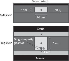
FIGURE 56.1 Schematic of the simulated nanowire MOSFET device, where the position of the trap/impurity atom is indicated.
The incorporation of self-heating effects in the existing model is achieved by self-consistently solving a multiband 3D Monte Carlo/MD coupled to a 3D Poisson equation solver, which is then self-consistently coupled with 3D energy balance equations for the acoustic and optical phonons [8, 9 and 10]. A schematic of the complete program flowchart is given in Figure 56.2. Briefly, after specifying the structure and relevant input parameters, an equilibrium 3D Poisson equation is solved given the applied gate bias. Then a charge assignment is performed and the Monte Carlo free-flight scatter procedure is initiated. During the carrier free-flights, carriers are accelerated according to the electric fields that result from the solution of the 3D Poisson equation (long-range portion of the Coulomb interaction) + electric fields that arise from particle–particle–particle–mesh coupling (short-range portion of the Coulomb interaction). The ensemble Monte Carlo (EMC)–Poisson–MD routine is run for 10 ps, after which the energy balance equations are solved for the optical and the acoustic phonon bath temperature profiles. It is necessary to incorporate separately the acoustic and the optical phonon baths due to the different timescales involved in the energy transfer processes involved, as schematically depicted in Figure 56.3. The information for the local acoustic and optical phonon temperatures is used in the Monte Carlo free-flight scatter routine, in the choice of the scattering mechanism (scattering tables). When the EMC–MD–Poisson sequence is complete, the information about the local electron density, electron temperature, and the electron drift velocity is inputted into the energy balance solver to calculate the corresponding lattice temperature and optical phonon temperature profiles.
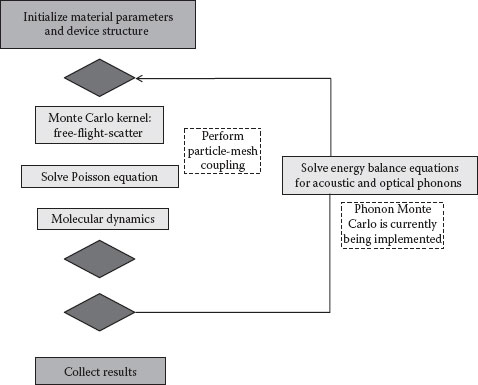
FIGURE 56.2 Flowchart of the Monte Carlo–molecular dynamics–3D Poisson–3D thermal solver.
When solving the energy balance equations for the acoustic and optical phonons, boundary conditions on the lattice temperature must be established. Recalling that there is an analogy between the electrical and thermal variables, from Ohm’s law for electrical conduction and Fourier’s law for heat conduction, one immediately sees that electrostatic potential is analogous to lattice temperature and electrical current is analogous to heat flux. We know that when solving the Poisson equation for electrostatic potential, one has to define at least one node on the Poisson mesh with Dirichlet boundary conditions to connect to the outside world. Hence, in the lattice temperature mesh, at least one node has to have Dirichlet boundary conditions. In all the simulations presented in this chapter, the bottom (substrate) electrode is taken to be at lattice temperature T = 300 K and the top gate is also assumed to be at temperature T = 300 K. For all the other boundaries, Neumann boundary conditions are assumed.
In Table 56.1, we show simulation results for the case when a negative trap is placed right at the source end of the channel or 1 nm inside the channel toward the gate. From the results presented in Table 56.1, it is evident that larger current degradation is observed for the case when the trap is located 1 nm into the channel, namely, when the trap is at the source end of the channel, the current degradation is 0.47% and when the trap is located 1 nm in the channel, the current degradation is 2.12%, a factor of five higher. The explanation to this behavior is as follows: when the trap is located at the source end of the channel, screening from the source electrons is very effective in reducing the strength of the trap’s Coulomb potential. Therefore, the current that flows through the structure is reduced by a negligible amount. More current means more self-heating effects, which can be observed from the lattice and optical temperature plots shown in Figure 56.4. In other words, maximum lattice temperature is 399 K when the trap is located right at the source end and is reduced to 397 K when the trap is moved 1 nm into the channel.
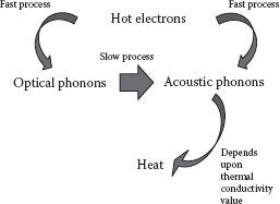
FIGURE 56.3 Most likely energy loss paths for energetic particles in a semiconductor device. (D. Vasileska, A. Hossain, and S. M. Goodnick, Self-heating and short-range coulomb interactions due to charging of traps in nanowire transistors, in Proceedings of the 2011 IEEE Nano Conference on Nanotechnology, Portland, Oregon, pp. 1110–1113. © (2011) IEEE. With permission.)
TABLE 56.1
Single Negative Impurity Impact on Current Degradation
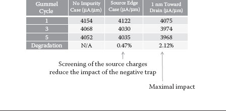
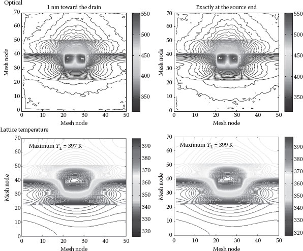
FIGURE 56.4 Optical (top panel) and lattice (bottom panel) temperature profiles for the case of a negative impurity placed 1 nm into the channel (left panels) and a negative impurity placed at the source edge of the channel (right panels). Applied bias is VGS = VDS = 1.2 V.
In summary, we have presented simulation results for the degradation of the ON current in the presence of a negatively charged impurity placed in the middle of the source end injection barrier. We find that the interplay of self-heating and Coulomb effects is very complicated in nanowire transistors and both have to be accounted for to get proper estimates of the ON current.
1. M. J. Kirton and M. J. Uren, Noise in solid-state microstructures: A new perspective on individual defects, interface states and low frequency (1/f) noise, Advances in Physics, 38, 367–468, 1989.
2. K. S. Ralls, W. J. Skocpol, L. D. Jackel, R. E. Howard, L. A. Fetter, R.W. Epworth, and D. M. Tennat, Discrete resistance switching in submicrometer silicon inversion layers: Individual interface traps and low-frequency (1/f) noise, Physical Review Letters, 52(3), 228–231, 1984.
3. H. Kurata, K. Otsuga, A. Kotabe, S. Kajiyama, T. Osabe, Y. Sasago, S. Narumi, K. Tokami, S. Kamohara, and O. Tsuchiya, The impact of random telegraph signals on the scaling of multilevel flash memories, in Proceedings of the Symposium on VLSI Circuits, 125–126, 2006.
4. D. Vasileska and S. S. Ahmed, Narrow-width SOI devices: The role of quantum mechanical size quantization effect and the unintentional doping on the device operation, IEEE Transactions on Electron Devices, 52, 227236, 2005.
5. W. J. Gross, D. Vasileska, and D. K. Ferry, A novel approach for introducing the electron-electron and electron-impurity interactions in particle-based simulations, IEEE Electron Device Letters, 20, 463–465, 1999.
6. Z. Aksamija and I. Knezevic, Anisotropy and boundary scattering in the lattice thermal conductivity of silicon nanomembranes, Physical Review B, 82, 045319, 2010.
7. D. Li, Y. Wu, P. Kim, L. Shi, P. Yang, and A. Majumdar, Thermal conductivity of individual silicon nanowires, Applied Physics Letters, 83, 2934–2936, 2003.
8. D. Vasileska, K. Raleva, and S. M. Goodnick, Self-heating effects in nano-scale FD SOI devices: The role of the substrate, boundary conditions at various interfaces and the dielectric material type for the BOX, IEEE Transactions on Electron Devices, 56(12), 3064–3071, 2009.
9. D. Vasileska, K. Raleva, and S. M. Goodnick, Modeling heating effects in nanoscale devices: The present and the future, Journal of Computational Electronics, 7(2), 66–93, 2008.
10. D. Vasileska, A. Hossain, and S. M. Goodnick, The role of the source and drain contacts on self-heating effect in nanowire transistors, ECS Transactions, 31, 83–91, 2010.
11. D. Vasileska, A. Hossain, and S. M. Goodnick, Self-heating and short-range coulomb interactions due to charging of traps in nanowire transistors, in Proceedings of the 2011 IEEE Nano Conference on Nanotechnology, Portland, Oregon, pp. 1110–1113, 2011.