
Impact of Phonon Scattering in an Si GAA Nanowire FET with a Single Donor in the Channel |
CONTENTS
57.2 Nonequilibrium Green’s Function Model.
57.3 Electron–Electron Interaction Model beyond the Hartree Approximation
57.5 Effect of Single Dopant on Performance of NFET
Nanowire field effect transistors (NFETs), FinFETs, and other 3D architectures are progressively replacing the bulk metal-oxide semiconductor field-effect transistor (MOSFET) architecture in a complementary metal-oxide semiconductor (CMOS) Si technology. This process has been started by Intel’s introduction of TriGate (a variant of FinFET) MOSFET architecture into high-volume production of the 22 nm technology node [1]. The superior electrical integrity of FinFETs and nanowires resulting in very low leakage current at the off-state, as compared to much leakier bulk architectures, is the main reason for this trend [2]. However, when the transistor cross section and channel lengths reach sub-10 nm dimensions, quantum effects such as confinement, gate tunneling, and source/drain (S/D) tunneling will dominate over classical electrostatic alternately affecting the electrostatic integrity of 3D device architectures. Therefore, we deploy nonequilibrium Green’s function (NEGF) [3] simulations to study the effect of a single dopant unintentionally present in the channel of an NFET [4]. The probability of occurrence of this unintentional dopant will also increase in devices with sub-10 nm dimensions.
The NEGF simulations include a phonon scattering considering the electron interactions with acoustic and nonpolar optical phonons dominant in silicon [5], unlike previous studies investigating the effect of the single dopant [6,7]. Even though phonon scattering has already been incorporated into NEGF simulations of nanowire transistors [8, 9 and 10], its effect on the single dopant in a nanowire has not been studied. Furthermore, the separate impact of elastic and inelastic phonon scatterings has not been looked at. Therefore, we study the effect of phonon scattering on the Si NFET with the single dopant close to the source. The donor is introduced as a charge distribution and the potential is calculated self-consistently within a Hartree approximation. The asymmetrical location of the donor in the middle of the channel allows the electrons near the source to tunnel into the donor potential and then be heated up to the top of the potential barrier via inelastic phonon processes.
57.2 NONEQUILIBRIUM GREEN’S FUNCTION MODEL
The NEGF formalism within one-electron approximation reduces a many-body Schrödinger equation to a solution of the following equations [3,11]:
(57.1) |
(57.2) |
where g0 is the retarded Green’s function for a single-electron part of a Hamiltonian with the external field U turned off, and σ is the retarded self-energy including the coupling to leads and other interactions (i.e., the electron–phonon interactions). The g and ga are the retarded and advanced Green’s functions, respectively. In Equation 57.2, g< and σ < are “the-lesser-than” pieces of the complex contour path of Green’s function (i.e., the first leg is always in earlier time than the second leg in the complex contour [3]). The Hamiltonian of NEGF is written in the effective mass approximation and the effective mass itself is extracted from tight-binding calculations [12] (ml =1.07, mt = 0.3 in units of electron mass), which accounts for a bandstructure change due to strong confinement occurring in the nanowires. In other words, Equation 57.1 is equivalent to the Schrödinger equation in single-electron approximation and Equation 57.2 is a quantum generalization of the semiclassical Boltzmann equation. The contacts are assumed to be in equilibrium and at room temperature. We employ a recursive algorithm [13] that allows us to calculate only the diagonal and first off-diagonal blocks of the less-than Green’s function g<. g< is then required for the computation of current and electron density in the NEGF formalism [3].
57.3 ELECTRON–ELECTRON INTERACTION MODEL BEYOND THE HARTREE APPROXIMATION
The incorporation of an electron–electron interaction into a single-electron model is a cumbersome task [3]. One of the most practical ways based on a set of theorems had been introduced by Kohn and Sham [14] who proposed their famous one-electron Schrödinger equation in the following form:
(57.3) |
where is a kinetic operator and m(r) is the position-dependent mass. V(r) is the Coulomb potential given by
(57.4) |
where v(r) is the electrostatic, external potential, ρ(r) is the ground-state density, and r represents x, y, z coordinates in a real space. Finally, vXC(r) is an exchange–correlation (XC) potential [14] generally defined as the difference between a full, many-body kinetic plus potential energy and one-body kinetic plus potential energy. The XC potential is impossible to express for large, many-body systems like NFETs, but there are various physical approximations like the local density approximation (LDA) or the generalized gradient approximation (GGA) that can serve. The accuracy of these approximations is quite strongly dependent on the nature of the physical system and physical quantities one would like to compute. Therefore, these approximations are typically suitable for particular calculations performed in solid-state physics (energy band calculations of metals, semiconductors, insulators, ferromagnetic materials, calculations of material permittivity, etc.). The analytical parametrization introduced by Hedin and Lundqvist [15] has proven to be the most practical with sufficient accuracy for a large number of solid-state problems related to semiconductors. In this parametrization, the XC potential is split into two parts, the first being the exchange plus correlation hole, and the second being the correlation energy correction to chemical potential, as follows [15]:
(57.5) |
where X = rs/21. This XC potential parametrization is valid for a wide range of rs, while rs is defined via a local carrier density n(r) as
and
where εsc is the permittivity of a semiconductor and ε0 is the permittivity of a vacuum. In silicon, rs values span a range of 2.6–0.26, corresponding to electron concentrations of 1018–1021 cm−3. The XC potential can then be relatively easily included into self-consistent simulations of carrier transport in semiconductor devices by adding it to the electrostatic potential v(x,y,z) [16,17] since the carrier density n(r) is often known locally. In our NEGF simulation approach, the electron density n(x,y,z) entering the XC potential is obtained from self-consistent simulations iteratively solving the NEGF and Poisson equations. The XC potential is plotted in Figure 57.1 as a function of the carrier density showing the contribution due to the exchange only (LDA) and the exchange–correlation (Hedin–Lunqvist) parts represented by the first and second terms in the last square brackets of Equation 57.5, respectively. The XC potential induces a 20–80 meV shift in the electron self-energy at the carrier density typical in Si NFETs. This shift is more significant in the access regions to the channel, where the carrier density approaches 1020 cm−3, inducing a lowering of the S/D barrier and thus increasing the on-current as indicated in Figure 57.2. Figure 57.2 demonstrates that the potential profile given by conduction band edge substantially decreases the potential barrier between the source and the drain. Note also that the potential in the source and the drain practically do not change. The XC potential-induced self-energy shift is of the order of threshold voltage shift induced by statistical sources of fluctuations [2,4] such as random dopants and surface roughness and thus should be considered as an accurate description of carrier transport.
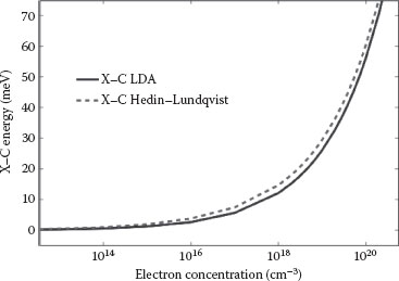
FIGURE 57.1 The XC potential approximation of Ref. [15] compared with the standard local density approximation (LDA). The difference between the two potentials is smaller than 6 meV in the range of relevant electron densities in Si transistors. (A. Martinez, K. Kalna, and M. Aldegunde, Impact of phonon scattering in a Si GAA nanowire FET with a single donor in the channel, Proc. 11th IEEE International Conference on Nanotechnology, August 15–18, 2011, Portland, Oregon, pp. 1348–1351. © (2011) IEEE. With permission [18].)
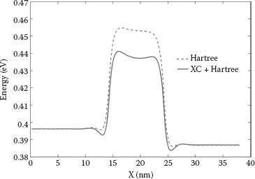
FIGURE 57.2 Potential energy across the channel of Si NFET at equilibrium including and excluding the XC potential at VD = 0.01 V. (A. Martinez, K. Kalna, and M. Aldegunde, Impact of phonon scattering in a Si GAA nanowire FET with a single donor in the channel, Proc. 11th IEEE International Conference on Nanotechnology, August 15–18, 2011, Portland, Oregon, pp. 1348–1351. © (2011) IEEE. With permission [18].)
The gate-all-around (GAA) nanowire transistor considered in this chapter is schematically shown in Figure 57.3. It has 14 nm long S/D regions and a 10 nm channel length. It has a square cross section of 2.2 × 2.2 nm2 coated with a 0.8 nm SiO2 dielectric layer providing a confinement potential of 3.1 eV. The channel is undoped and the S/D regions have an n-type doping concentration of 1020 cm−3. A metal gate is wrapped all around the nanowire on the outer surface of the oxide and is assumed to have a work function of 4.5 eV.
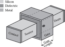
FIGURE 57.3 Schematic view of the considered Si NFET with the indicated position of the single dopant in the channel (a dark dot).
We would like to stress that phonon scattering is considered in the whole device, including the S/D regions and not just in the channel as in many previous studies [6,8]. This approach makes the device simulations much more realistic since the electron interaction with phonons plays a considerable role in the heavily doped S/D regions despite the frequent interactions with ionized impurities.
57.5 EFFECT OF SINGLE DOPANT ON PERFORMANCE OF NFET
Figure 57.4 shows the ID–VG characteristics of a pristine nanowire transistor both in the presence and absence of phonon scattering (all the simulations are done at VD = 10 mV). To isolate the effect of inelastic scattering, we also show the ID–VG characteristics in which we consider all the scattering mechanisms as elastic. An expected result is that elastic scattering produces a lower current than inelastic scattering. This is partially a consequence of the impossibility of electrons being heated in the source and cooled in the drain because the emission or absorption of phonons is prohibited. In the case of inelastic scattering, the electrons, cooled in the drain, have a small chance to return to the source and therefore to contribute to an increase in the current, as opposed to a more realistic simulation in which we consider phonon scattering to be elastic. Figure 57.5 shows the corresponding cases but with the impurity located 3 nm from the source/channel interface.
The overall effect of phonon scattering is less severe, as shown in Figure 57.6. Figure 57.6 shows the percentage decrease in the ballistic current due to phonon scattering in a pristine device and a device with a donor in the channel. A case of the NFET with a donor in the channel considering only the elastic phonon scattering is shown for comparison. Figure 57.6 also shows that, in a pristine wire, the scattering increases as the gate bias increases but an impurity in the channel behaves unexpectedly. The energy states induced by the single dopant into the nanowire channel can completely remove the effect of phonon scattering and increase the current to its ballistic value, as seen in Figure 57.6 at VG = 0.6 V. The resonant level here has a major impact on the current and the optical phonon scattering maximizes the absorption of carriers in the source.
Finally, our results predict a decrease in the on-current of more than 70% for the pristine wire due to phonon scattering. The current reduction is slightly smaller if the device has a donor positioned in the middle of the channel. This result is partially due to the increase in electron tunneling from the source to the drain in the presence of a single donor in the channel.
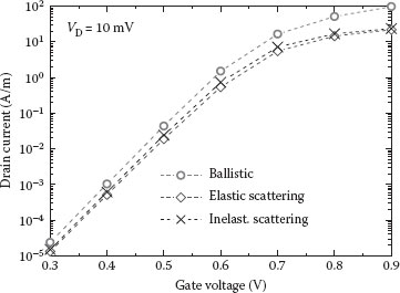
FIGURE 57.4 ID–VG characteristics of the 10 nm gate length pristine Si nanowire. The ballistic NEGF simulations are compared with the simulations, which include elastic and inelastic phonon scattering. (A. Martinez, K. Kalna, and M. Aldegunde, Impact of phonon scattering in a Si GAA nanowire FET with a single donor in the channel, Proc. 11th IEEE International Conference on Nanotechnology, August 15–18, 2011, Portland, Oregon, pp. 1348–1351. © (2011) IEEE. With permission [18].)
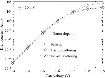
FIGURE 57.5 ID–VG characteristics of the same Si nanowire simulated with ballistic NEGF and NEGF, including elastic and inelastic phonon scattering. (A. Martinez, K. Kalna, and M. Aldegunde, Impact of phonon scattering in a Si GAA nanowire FET with a single donor in the channel, Proc. 11th IEEE International Conference on Nanotechnology, August 15–18, 2011, Portland, Oregon, pp. 1348–1351. © (2011) IEEE. With permission [18].)
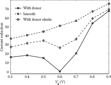
FIGURE 57.6 Current reduction in the NFET at VD = 0.01 V due to the phonon scattering against the ballistic transport model for a pristine nanowire (Smooth), with a single dopant including only elastic scattering (with donor Elastic), and with a single dopant including all scatterings (with donor). (A. Martinez, K. Kalna, and M. Aldegunde, Impact of phonon scattering in a Si GAA nanowire FET with a single donor in the channel, Proc. 11th IEEE International Conference on Nanotechnology, August 15–18, 2011, Portland, Oregon, pp. 1348–1351. © (2011) IEEE. With permission [18].)
Figure 57.7 shows the electron density at VG = 0.6 V, illustrating the sharp peak of the density along the channel induced by the single dopant. The peak of the density is reflected in the local density of states (LDoS) and in the current spectra along the axis of the nanowire at VG = 0.6 V shown in Figures 57.8 and 57.9. The LDoS in Figure 57.8 indicates the resonant level of the impurity potential as well as the induced resonances into the density of states. The current spectra in Figure 57.9 illustrate clearly two conduction channels created by the split due to the single dopant in the channel. At this gate bias of VG = 0.6 V, the contribution of the resonant state to the total current is 7%, but at VG = 0.7 V, the resonant state contribution increases to about 30%. The heating and the cooling of carriers, indicated by the red and blue colors for the high and low energy of carriers, can also be seen in Figure 57.9. The heated carriers are accumulated just above the wide barrier near the drain created by the single dopant. One can also see how they then quickly cool down when entering the drain region.
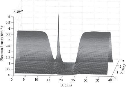
FIGURE 57.7 Electron density along the nanowire at VG = 0.6 V and VD = 0.01 V. The source and the drain are uniformly n-type doped up to 1020 cm−3 and the single dopant is placed in the middle of the channel, 3 nm from the source. (A. Martinez, K. Kalna, and M. Aldegunde, Impact of phonon scattering in a Si GAA nanowire FET with a single donor in the channel, Proc. 11th IEEE International Conference on Nanotechnology, August 15–18, 2011, Portland, Oregon, pp. 1348–1351. © (2011) IEEE. With permission [18].)
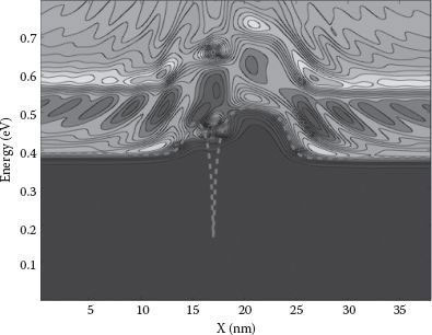
FIGURE 57.8 Local density of states (LDoS) along the axis of the nanowire at VG = 0.6 V and VD = 0.01 V.
Furthermore, we go beyond the standard Hartree–Fock approximation and simulate the impact of XC potential introduced in the previous section using the NEGF approach from Silvaco’s ATLAS toolbox [19]. The exchange takes into account that electrons are indistinguishable particles reducing thus the ground-state energy, and that the correlation improves the Hartree–Fock approximation accounting for the many-body effects. The resulting effective potential will then be lower than the potential excluding the exchange–correlation, and the density in the channel increases as observed mostly close to the threshold voltage. Figure 57.10 shows a comparison of ID–VG characteristics at a low drain voltage of 0.01 V. Note first that our in-house NEGF simulator gives ID–VG characteristics that are in excellent agreement with those obtained from Silvaco’s NEGF simulations in a ballistic regime. The lowering of the current due to the presence of the single dopant is also illustrated, assuming the same ballistic transport regime. When the XC potential is included in ballistic simulations, the current is not changed in the subthreshold region due to a low carrier density in the channel. However, when the gate bias drives the NFET into on-state, the current starts to increase more swiftly when the XC potential is included compared to the result when it is excluded.
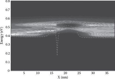
FIGURE 57.9 The current spectra along the axis of the nanowire at VG = 0.6 V and VD = 0.01 V. (A. Martinez, K. Kalna, and M. Aldegunde, Impact of phonon scattering in a Si GAA nanowire FET with a single donor in the channel, Proc. 11th IEEE International Conference on Nanotechnology, August 15–18, 2011, Portland, Oregon, pp. 1348–1351. © (2011) IEEE. With permission [18].)
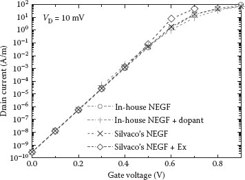
FIGURE 57.10 ID–VG characteristics at VD = 0.01 V of the 10 nm gate length Si nanowire simulated with our ballistic NEGF (in-house) w/o dopant compared with Silvaco’s ATLAS NEGF in a ballistic regime and also including exchange and correlation (Ex).
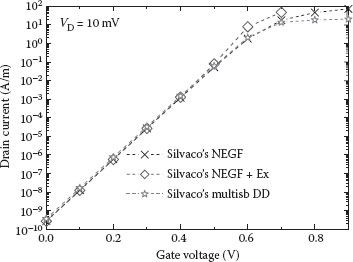
FIGURE 57.11 ID–VG characteristics at VD = 0.01 V of the pristine Si nanowire comparing the ATLAS NEGF simulations in a ballistic regime with/without the exchange and correlation (Ex) to multi-subband drift-diffusion simulations (multisb DD). (A. Martinez, K. Kalna, and M. Aldegunde, Impact of phonon scattering in a Si GAA nanowire FET with a single donor in the channel, Proc. 11th IEEE International Conference on Nanotechnology, August 15–18, 2011, Portland, Oregon, pp. 1348–1351. © (2011) IEEE. With permission [18].)
Finally, Figure 57.11 shows a comparison of the results obtained from drift-diffusion (DD) multisubband simulations [19]. The results confirm the same electrostatic behavior by exhibiting the same subthreshold slope. However, the on-current obtained from the DD multi-subband simulations of Silvaco’s ATLAS toolbox is lower. This is because the carrier scattering in the DD is taken into account through a mobility model, while the NEGF simulations of Silvaco ATLAS were carried out in a ballistic regime. The ballistic simulation will thus predict a much larger current since this model assumes that electrons do not scatter and thus cannot lose their kinetic energy (gained from the electric field present in the channel). Furthermore, the DD multi-subband Silvaco simulations show a very similar on-current with a difference of only 10% when compared to the on-current obtained from the corresponding in-house NEGF simulations with the phonon scattering included as presented in Figure 57.10. We are not able to draw any conclusions on this close agreement as to speculate that this is due to a decisive effect of the electron density along the nanowire channel on the current while the electron dynamics (electron drift velocity/mobility) plays a less important role in determining this current at VD = 0.01 V.
3D NEGF simulations including dissipative processes due to elastic and inelastic phonon scattering have been carried out to investigate its effect on device characteristics of a 10 nm gate length Si NFET with a cross section of 2.2 × 2.2 nm2. Compared to previous studies of NFETs, we have investigated the effect of dissipative processes in the nanowire with and without a single dopant in the channel, also taking into account the impact of heavily doped S/D access regions. The role of the elastic and inelastic phonon scatterings in electron transport has been compared with the results from ballistic NEGF simulations. We have found that the presence of the dopant in the channel close to the source region reduces the impact of phonon scattering on the drain current.
This phonon scattering reduction is the largest at the gate voltage at which the resonant level of the impurity has the maximum impact on the drain current. The contribution of the electron tunneling current, enhanced by the resonant level of impurity, is the largest relative to the total current. In other words, the effect of phonon scattering on the current has become negligible at the gate bias at which a relatively large amount of electrons are transmitted from the source to the drain through the impurity-induced resonant level. Phonon scattering has been included not only into the channel but also into the heavily doped S/D, thus distinguishing these simulations as much more realistic.
We have also evaluated the impact of the XC potential in a pristine NFET. The results show that the inclusion of the XC potential increases the on-current more than twice but has little impact on the subthreshold regime. This behavior is consistent with the decrease of overall potential energy in the channel of the nanowire due to the inclusion of the XC potential and with the fact that the overall potential in the heavily doped S/D remains unaltered.
This work was supported by EPSRC grants EP/I004084 and EP/D070236.
1. http://www.intel.com/content/www/xa/en/silicon-innovations/intel-22nm-technology.html, 2011.
2. D. Hisamoto, W.-C. Lee, J. Kedzierski, E. Anderson, H. Takeuchi, K. Asano, T.-J. King, J. Bokor, and C. Hu, A folded-channel MOSFET for deep-sub-tenth micron era. Int. Electron Devices Meeting Tech. Dig., pp. 1032–1034, 1998.
3. S. Datta, Electronic Transport in Mesoscopic Systems, Cambridge University Press, Cambridge, UK, 1995.
4. A. Martinez, M. Bescond, J. R. Barker, and A. Svizhenko, M. P. Anantram, C. Millar, and A. Asenov, A self-consistent full 3-D real-space NEGF simulator for studying nonperturbative effects in nano-MOSFETS, IEEE Trans. Electron Devices 54, 2213–2222 (2007).
5. C. Jacoboni and P. Lugli, The Monte Carlo Method for Semiconductor Device Simulations, Springer, Wien-N.Y. 1989.
6. M. Bescond, M. Lannoo, L. Raymond, and F. Michelini, Single donor induced negative differential resistance in silicon n-type nanowire metal-oxide-semiconductor transistors, J. Appl. Phys. 107, 093703-1-6, 2010.
7. A. Martinez, N. Seoane, M. Aldegunde, A. R. Brown, J. R. Barker, and A. Asenov, 3-D nonequilibrium Green’s function simulation of nonperturbative scattering from discrete dopants in the source and drain of a silicon nanowire transistor, IEEE Trans. Nanotech. 8, 603–610, 2009.
8. S. Jin, Y.-J. Park, and H. S. Min, A three-dimensional simulation of quantum transport in silicon nanowire transistor in the presence of electron-phonon interactions, J. Appl. Phys. 99, 123719-1-123719-10, 2006.
9. A. Svizhenko and M. P. Anantram, Role of scattering in nanotransistors, IEEE Trans. Electron Devices 50, 1459–1466, 2003.
10. M. Luisier and G. Klimeck, Atomistic full-band simulations of silicon nanowire transistors: Effects of electron-phonon scattering, Phys. Rev. B 80, 155430, 2009.
11. D. C. Langreth and J. W. Wilkins, Theory of spin resonance in dilute magnetic alloys, Phys. Rev. B 6, 3189–3227, 1972, Equations 57.1 and 58.2 correspond to Equations A15–A16.
12. K. Nehari, N. Cavassilas, J. L. Autran, M. Bescond, D. Munteanu, and M. Lannoo, Influence of band structure on electron ballistic transport in silicon nanowire MOSFET’s: An atomistic study, Solid-St. Electron. 50, 716–721, 2006.
13. A. Svizhenko, M. P. Anantram, T. R. Govindan, B. Biegel, and R. Venugopal, Two-dimensional quantum mechanical modeling of nanotransistors, J. Appl. Phys. 91, 2343–2354, 2002.
14. W. Kohn and J. Sham, Phys. Rev. 140, A1133–1138, 1965; J. Sham and W. Kohn, Phys. Rev. 145, 561–567, 1966.
15. L. Hedin and B. I. Lundqvist, Explicit local exchange-correlation potentials, J. Phys. C: Solid St. Phys. 4, 2064–2083, 1971.
16. H. Iwata, T. Matsuda, and T. Ohzone, Influence of image and exchange-correlation effects on electron transport in nanoscale DG MOSFETs, IEEE Trans. Electron Devices 52, 1596–1602, 2005.
17. D. Vasileska, D. K. Schroder, and D. K. Ferry, Scaled silicon MOSFETs: degradation of the total gate capacitance, IEEE Trans. Electron Devices 44, 584–1587, 1997.
18. A. Martinez, K. Kalna, and M. Aldegunde, Impact of phonon scattering in a Si GAA nanowire FET with a single donor in the channel, Proc. 11th IEEE International Conference on Nanotechnology, August 15–18, 2011, Portland, Oregon, pp. 1348–1351.
19. Silvaco Int., Atlas User’s Manual [online]. Available: www.silvaco.com.