
Modeling and Minimizing Variations of Gate-All-Around Multiple-Channel Nanowire TFTs |
CONTENTS
Although polysilicon thin-film transistors (poly-Si TFTs) are attracting much attention for their use in active-matrix liquid crystal displays [1,2], fine-grain structures in the channel can affect their carrier transport and device performance. Poly-Si consists of a number of single-crystal grains. Between poly-Si grains, there exists a high defect density region called the grain boundary with a typical value of defect density ca. 1012 cm−2. Such a large number of randomly oriented grain boundaries usually cause large variations in the device’s electrical characteristics, including the threshold voltage and subthreshold swing (SS) [3]. Hence, several methods, including excimer laser annealing [4] and metal-induced lateral crystallization [5], have been developed to increase the grain size and minimize the grain boundary defects and thereby improve the electrical characteristics of poly-Si TFTs. Recently, a multiple-gate structure was reported in which the additional electric field enhanced the control over the channel surface potentials and the device performance, providing improved immunity to short channel effects [6,7]. In addition, TFT characteristics are dramatically improved upon reducing the channel width, particularly when using a nanowire (NW) as a channel [8,9]. Poly-Si TFTs featuring multiple NW channels exhibit improved performance relative to that of traditional planar devices because of the increment of effective channel width and the reduced grain boundary trap density in the channel region [10,11]. When the channel width and the poly-Si grain size are of the same order of magnitude, the random distribution of the grain boundary causes an even greater electrical fluctuation including threshold voltage and SS [9,12,13]. Therefore, uniformity of the grain boundary is critical when scaling down device dimensions.
In a previous study [7], we found that a gate-all-around (GAA) poly-Si NW TFT exhibited excellent gate controllability because the GAA structure enhanced the electric field. In this study, we investigated the performance of GAA NW TFTs featuring multiple gate configurations; in particular, we compared the tri-gate and GAA structures and studied the impact of multiple channels to further reduce the fluctuations in device performance. Indeed, the variations in threshold voltage and SS were effectively modulated. Although the Poisson area scatter model was proposed to estimate the impact of statistical grain boundary distribution on TFT characteristics [14]. To the best of our knowledge, this model has never been adopted to model poly-Si GAA TFTs featuring multiple NW channels, especially for devices with a grain size and channel diameter in the same order of magnitude. Finally, we found that NH3 plasma treatment further minimized the fluctuations and improved the performance of these GAA NW TFTs.
The 1-µm-long multiple channels of the poly-Si NWs were fabricated using a spacer patterning technique [7]. At first, a 75-nm-thick undoped amorphous-Si (α-Si) layer was deposited onto a 200-nm-thick bottom oxide (BOX) at 550°C using low-pressure chemical vapor deposition (LPCVD). In sequence, solid-phase crystallization (SPC) was performed at 600°C for 24 h in a nitrogen ambient to turn the α-Si into a polycrystalline Si structure. The key parameter of the spacer patterning technique was the thickness of followed deposition of the tetraethylorthosilicate (TEOS) oxide and nitride spacer. The TEOS oxide thickness defined the height of the nitride spacer. After definition of the TEOS pattern by reactive ion etching (RIE), the nitride was deposited and then etched using RIE. The thickness of the nitride film corresponded to the width of the spacer. In the study, the thicknesses of the TEOS and nitride layers were chosen to be 70 and 60 nm, respectively, for these processing conditions. Using the nitride spacer as a hard mask, 1-µm-long multiple channels of poly-Si NW having a channel width (Wch) of 44 nm were formed. By varying the thicknesses of the TEOS and nitride layers, nanoscale structures were readily defined without the need for advanced lithography techniques. After wet etching in a diluted HF solution (1:100) to remove the 70–80 nm BOX layer, the poly-Si NW was released from the BOX substrate. Next, the sequential conformal deposition (LPCVD) of dielectric of oxide-nitride-oxide (ONO) stacks (TEOS/nitride/TEOS = 10.5 nm/5.5 nm/15.3 nm) and 200-nm-thick in situ N+ poly-Si was performed to surround the channels. After gate pattern transformation, the etching of dielectric on the source and drain surface was performed. The self-aligned phosphorus ion implantation was then completed at a dose of 5 × 1015 cm−2 for the formation of ohmic contact. The TEOS passivation, thermal annealing (600°C, 6 h), standard metal contact formation, and sintering processes were performed to provide the final structure. To study the impact of the grain boundary defects, the samples were subjected to NH3 plasma treatment in a parallel-plate plasma reactor at a power density of 0.7 W/cm2 at 300°C for 1 h.
Figure 58.1 presents transmission electron microscopy (TEM) images of NW channels possessing a GAA structure and a tri-gate structure surrounded by ONO layers. These devices had a nominal channel length (L) of 1 µm (effective channel length ~ 0.75 µm), a channel width (Wch) of 44 nm, and a channel thickness (Tch) of 62 nm. The ONO stack (O/N/O = 10.5 nm/5.5 nm/15.3 nm) was conformably deposited around the channel. Such a stack layer can improve the future integrating memory function when using a system-on-panel (SOP) approach [15]. To prevent the effects of nonuniformity of our fabricated NWs, especially during the film deposition and etching processes, the devices under investigation were selected from the same vicinity of the chip.
Figure 58.2 presents the transfer curves of the GAA and tri-gate NW TFTs. Relative to the tri-gate device, the GAA NW TFT, even when it had not been subjected to the treatment process, suppressed the short channel effects (SCEs), providing a smaller drain induce barrier lowering (DIBL), a lower leakage current, and a steeper SS, because the GAA devices provided additional electric field strength at the corner and bottom regions, leading to improvements in the values of the drain current and Vth [the gate voltage required to yield a normalized drain current of Id (W = L) = 10 nA at Vd = 0.1 V]. These improvements were also as a result of the channel potential being tightly controlled by the surrounding electric field. Moreover, the large number of trap states in the poly-Si channel region also played a critical role influencing the device performance and the SCEs. As a result, the poly-Si TFT exhibited a large leakage current due to the large field emission current near the drain side and grain boundary trap states in the channel [16]. Thus, after treatment process, the N and H atoms passivated the traps on the channel surface and/or in the channel area [7]. The passivation species diffused mainly through the gate oxide into the channel from the channel edge. These passivation radicals also further reduced the grain boundary potential barrier; hence, the off-state leakage current was minimized and the on-state current was enhanced. As a result, the proposed device exhibited a higher on/off current ratio (>108) than that of the untreated samples (>107). Therefore, the GAA NW TFT that had been subjected to NH3 plasma treatment exhibited improved device characteristics, including a lower value of Vth (0.18 V), a steeper SS (184 mV/dec), a very high on/off current ratio (1.64 × 10⁸), and a small DIBL (58 mV/V).
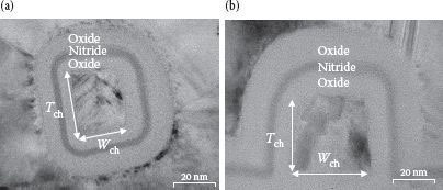
FIGURE 58.1 TEM images of (a) GAA and (b) tri-gate devices having a channel thickness of 44 nm and a channel width of 62 nm. The ONO stack (O/N/O = 10.5 nm/5.5 nm/15.3 nm) was prepared through conformal deposition using LPCVD. (Reprinted from Microelectronic Engineering, 91, P. C. Huang, L. A. Chen, C. C. Chen, and J. T. Sheu, Minimizing variation in the electrical characteristics of gate-all-around thin film transistors through the use of multiple-channel nanowire and NH3 plasma treatment, 54–58, (2012), with permission from Elsevier.)
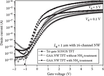
FIGURE 58.2 A comparison of transfer curves for GAA and tri-gate NW TFTs. After NH3 treatment, the GAA NW TFT exhibited superior performance. The GAA NW TFT that had been subjected to NH3 plasma treatment exhibited improved device characteristics, including a lower value of Vth (0.18 V), a steeper SS (184 mV/dec), a very high on/off current ratio (1.64 × 10⁸), and a small DIBL (58 mV/V). (Reprinted from Microelectronic Engineering, 91, P. C. Huang, L. A. Chen, C. C. Chen, and J. T. Sheu, Minimizing variation in the electrical characteristics of gate-all-around thin film transistors through the use of multiple-channel nanowire and NH3 plasma treatment, 54–58, (2012), with permission from Elsevier.)
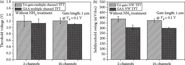
FIGURE 58.3 Mean values and standard deviations of the (a) threshold voltage and the (b) subthreshold swing of the GAA and tri-gate NW TFTs featuring 2 and 16 channels. (Reprinted from Microelectronic Engineering, 91, P. C. Huang, L. A. Chen, C. C. Chen, and J. T. Sheu, Minimizing variation in the electrical characteristics of gate-all-around thin film transistors through the use of multiple-channel nanowire and NH3 plasma treatment, 54–58, (2012), with permission from Elsevier.)
Figure 58.3a displays the mean values and the standard deviations of Vth for the different gate configurations possessing different numbers of channels. For the GAA NW TFTs possessing 2 and 16 channels, the mean values of Vth were 1.14 and 1.11 V, respectively; for the corresponding trigate devices, these values were 1.20 and 1.21 V, respectively. Notably, because the electric field surrounded the entire channel, the GAA NW TFT exhibited a smaller mean value of Vth relative to that of its tri-gate counterpart. In addition, the GAA NW TFT exhibited a smaller standard deviation of its value of Vth; such relative stability is critical for larger-glass active-matrix liquid crystal displays (AMLCD) applications. Furthermore, the grain boundaries of the SPC poly-Si were randomly distributed in the channel region, resulting in a variation of its electrical characteristics. These grain boundaries trap charges and build up potential barriers to the flowing carriers, resulting in additional scattering that leads to device degradation [17]. After SPC, the grain size in the channel region was approximately 25–40 nm in our experiment; relative to the NW channel having a value of Wch of 44 nm, we expected the device to suffer from fluctuating electrical characteristics, mainly due to these random distribution grain boundaries [12]. Our results reveal that the gate structure and the number of channels both influence the device characteristics. The standard deviations of the electrical characteristics of both the tri-gate and GAA NW TFTs were reduced effectively upon increasing the number of channels. The standard deviation of the value of Vth of the tri-gate TFT decreased from 174 to 82 mV; that of the GAA NW TFT decreased from 135 to 21 mV. Interestingly, the improvement of variation was greater when increasing the number of channels from 2 to 16 than it was when changing the gate configuration from a tri-gate to a surrounding gate. Figure 58.3b reveals similar results for the SS. The GAA NW TFT with 16 channels had the smallest average value (300 mV/dec) and standard deviation (9.38 mV/dec) of SS among all of the TFTs. Thus, the GAA structure improved the mean values of Vth and SS, and increasing the number of channels can effectively minimize the electrical variations.
Figure 58.4 displays the transfer characteristics of devices with channel numbers of 2, 4, 8, and 16. The transfer characteristics resulted from the measurements of 15 devices. Device-to-device variation was minimized by increase of channel numbers. On the basis of a previous study [14], the Poisson area scatter distribution was adopted to characterize the grain size variation relating to the properties of poly-Si GAA TFTs featuring multiple-channel NWs. An average grain area in the channel is assumed with an area of Ag. The active area of a transistor is defined by W × L. k is a Poisson random variable with an expected value of the number of grains, λ, within the active region. λ is defined by λ = (W × L)/Ag. For multiple channels, the channel width is defined as W = n × Weff, where n is the channel number and Weff is the effective channels width of an NW channel. The Poisson distribution probability P(k) with exactly k hits in an area W × L is defined as
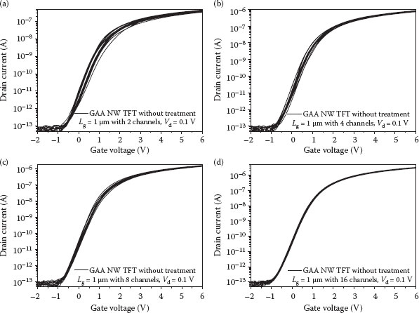
FIGURE 58.4 Transfer characteristics of GAA NW TFTs for channel numbers of (a) 2, (b) 4, (c) 8, and (d) 16. The uniformity of electrical characteristics has been effectively improved by increase of channel numbers. (Reprinted from Microelectronic Engineering, 91, P. C. Huang, L. A. Chen, C. C. Chen, and J. T. Sheu, Minimizing variation in the electrical characteristics of gate-all-around thin film transistors through the use of multiple-channel nanowire and NH3 plasma treatment, 54–58, (2012), with permission from Elsevier.)
(58.1) |
The average grain size within a specific transistor is also a random variable and is given by
(58.2) |
The threshold voltage is related to the grain size through the model [14,17]:
(58.3) |
Figure 58.5 exhibits the cumulative probability distributions of threshold voltage of a 2-channel poly-Si GAA TFT with different grain sizes. The threshold voltage is the minimum voltage when the grain boundary traps are filled. The significant conduction occurred only when all these traps were passivated. As a result, the larger the grain size the less the Vth, which presumably result from the fewer trapped levels that need to be filled. The larger the grain size, the smaller the Vth. However, a device with a larger grain size exhibits a larger electrical variation. Figure 58.6 presents the threshold voltage distribution related to the different channel numbers with an average grain size of 30 nm. The spread of Vth decreases as the channel number increases. This result exhibited that the statistics variation caused by grain size distribution has been balanced by the increasing channel numbers. Also, a comparison of magnitude of threshold voltage distribution from the experimental data and that calculated from the model shows a reasonable agreement as shown in the inset of Figure 58.6.
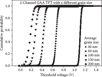
FIGURE 58.5 Cumulative probability distributions of threshold voltage for a 2-channel GAA TFT for different grain sizes; the effective channel length Leff is 0.75 μm. (P. C. Huang, L. A. Chen, C. C. Chen, and J. T. Sheu, Modeling and Minimizing Variations of Gate-All-Around Multiple-channel Nanowire TFTs, IEEE NANO 2011 Conference, August 15–18, 2011, Portland, Oregon. © (2011) IEEE. With permission.)
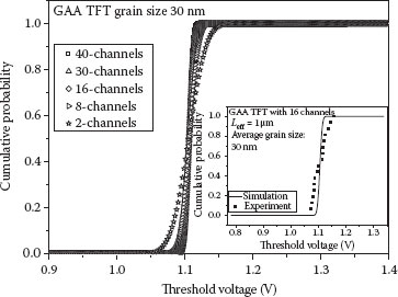
FIGURE 58.6 Cumulative probability distributions of threshold voltage for GAA NW TFTs featuring different channel numbers; grain size= 30 nm, Leff is 0.75 μm. Inset: Comparison of cumulative distributions of threshold voltage distribution in the experimental measurement data and the calculated model with 16 channels and effective channel length is 0.75 μm. (P. C. Huang, L. A. Chen, C. C. Chen, and J. T. Sheu, Modeling and Minimizing Variations of Gate-All-Around Multiple-channel Nanowire TFTs, IEEE NANO 2011 Conference, August 15–18, 2011, Portland, Oregon. © (2011) IEEE. With permission.)
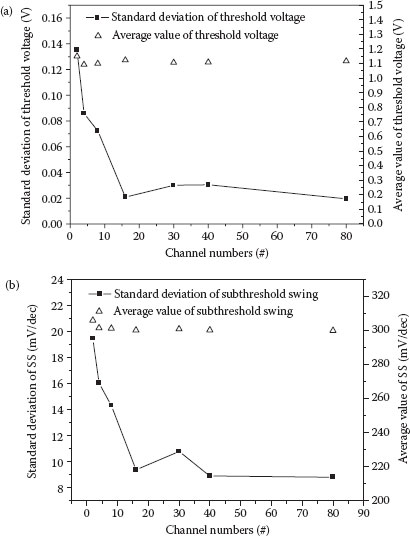
FIGURE 58.7 The electrical fluctuation has been minimized after devices featuring 16 channels. (a) The mean and standard deviation of the threshold voltage and (b) the mean value and standard deviation of subthreshold swing. The statistics were obtained from measurements of 15 GAA NW TFTs from three different chips, at Vd = 0.1 V. (Reprinted from Microelectronic Engineering, 91, P. C. Huang, L. A. Chen, C. C. Chen, and J. T. Sheu, Minimizing variation in the electrical characteristics of gate-all-around thin film transistors through the use of multiple-channel nanowire and NH3 plasma treatment, 54–58, (2012), with permission from Elsevier.)
Figure 58.7 shows the standard deviation and average value of threshold voltage and SS of devices with respect to the nanowire channel number. A device with 16 channels reaches a local minimum in both standard deviation of threshold voltage and SS (about 21 mV and 9.38 mV/dec, respectively). Figure 58.7a also shows that the average threshold voltage is around 1.1 V, and that extending the channel width by increasing the channel numbers did not affect the mobility for the constant current extraction method of Vth. Figure 58.7b exhibits a similar result of the SS, where the average value is maintained at 300 mV/dec with an increase in the channel number. However, the variation was reduced by increasing the channel number and reached a minimum value after utilizing 16 channels in our proposed device. Many crystallization technologies have been demonstrated to enlarge the grain size and to effectively reduce the impact of the grain boundary in the channel for device performance improvement [4,5]. However, it inherently brings a statistical variation induced by the grain boundary [18]. In this study, a multiple channel design provides a promising alternative to further improve the uniformity of electrical characteristics. Moreover, increasing the number of channels not only decreased the variation of the electrical properties but also improved the on/off current ratio (as shown in Figure 58.4), presumably due to the increase in the number of corners. However, the off-state leakage current remained tightly controlled by the surrounding electric field.
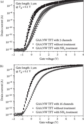
FIGURE 58.8 Transfer characteristics of GAA NW TFTs with (a) 2 and (b) 16 channels, with and without NH3 plasma treatment. I–V curves resulted from the measurements of 15 devices from three chips. (Reprinted from Microelectronic Engineering, 91, P. C. Huang, L. A. Chen, C. C. Chen, and J. T. Sheu, Minimizing variation in the electrical characteristics of gate-all-around thin film transistors through the use of multiple-channel nanowire and NH3 plasma treatment, 54–58, (2012), with permission from Elsevier.)
Figure 58.8 displays the transfer characteristics of GAA NW TFTs prepared with and without NH3 plasma treatment. The curves were then collected from different chips of the same batch. Five devices were characterized from each chip. The multiple-channel structure results in higher treatment efficiency relative to that of a traditional planar device [7]. According to the results shown in Figure 58.2, we observed that the threshold voltage and SS are all improved after NH3 plasma treatment, which reduced the trap states in the channel region. Moreover, the plasma passivation treatment also effectively reduces the electrical fluctuation. The 2-channel devices exhibited further minimization in standard deviation in their values of Vth (106 mV) and SS (15.88 mV/dec) compared to the untreated device (Vth is 135 mV and SS is 19.44 mV/dec) as shown in Figure 58.8a. Figure 58.8b shows that the treated 16-channel GAA NW TFT exhibits a very small value of standard deviation in its value of Vth and SS (30 mV and 11.4 mV/dec, respectively). In spite of that, NH3 plasma-treated 16-channel devices present a slight deterioration in electrical uniformity compared to the untreated ones; however, the device performance still shows obvious improvement.
We have characterized GAA NW TFTs featuring multiple channels to minimize the variation of their electrical characteristics. The gate structure and the number of channels both improved the device performance relative to that of tri-gate TFTs. Although the different gate configurations affected both the mean values and standard deviations of the performance metrics, increasing the number of channels decreased the grain boundary variation, effectively minimizing the electrical variations. To further improve the variations in device performance, devices were subjected to NH3 plasma treatment to reduce the trap density of states in the grain boundary. The proposed device of GAA NW TFT with 16 channels combined with plasma treatment exhibited a low threshold voltage (0.18 V), a steep SS (184 mV/dec), a high on/off current ratio (1.64 × 10⁸), a small DIBL (58 mV/V), and displayed a minimized standard deviation of Vth (30 mV) and SS (11.4 mV). The kink effect was also suppressed. Finally, we also utilize the Poisson area scatter model to characterize the electric variations of poly-Si NW TFTs with different grain size and channel numbers. The result shows a good agreement between the numerical simulation and experiment data. We suspect that such GAA multiple-channel TFTs would be suitable devices for applications in lowvoltage circuit operations.
We acknowledge the National Science Council, Taiwan, for financial support and the National Nano Device Laboratories for use of their facilities.
1. K. Yoneda, R. Yokoyama, and T. Yamada, Development trends of LTPS TFT LCDs for mobile applications, in VLSI Circuits, 2001. Digest of Technical Papers. 2001 Symposium on, Kyoto, Japan, 2001, pp. 85–90.
2. T. Aoyama, K. Ogawa, Y. Mochizuki, and N. Konishi, Inverse staggered poly-Si and amorphous Si double structure TFT’s for LCD panels with peripheral driver circuits integration, IEEE Transactions on Electron Devices, 43, 701–705, 1996.
3. Y. Nakajima, Y. Kida, M. Murase, Y. Toyoshima, and Y. Maki, Latest development of system-on-glass display with low temperature poly-Si TFT, Proc. SID Int. Symp. Dig. Tech. Papers, pp. 864–867, 2004.
4. A. Baiano, R. Ishihara, J. van der Cingel and K. Beenakker, Strained single-grain silicon n- and p-channel thin-film transistors by excimer laser, IEEE Electron Device Letters, 31, 308–310, 2010.
5. C.-W. Chang, S.-F. Chen, C.-L. Chang, C.-K. Deng, J.-J. Huang, and T.-F. Lei, High-performance nanowire TFTs with metal-induced lateral crystallized poly-Si channels, IEEE Electron Device Letters, 29, 474–476, 2008.
6. M. Im, J.-W. Han, H. Lee, L.-E. Yu, S. Kim, C.-H. Kim, S. C. Jeon et al., Multiple-gate CMOS thinfilm transistor with polysilicon nanowire, IEEE Electron Device Letters, 29, 102–105, 2008.
7. J.-T. Sheu, P.-C. Huang, T.-S. Sheu, C.-C. Chen, and L.-A. Chen, Characteristics of gate-all-around twin poly-Si nanowire thin-film transistors, IEEE Electron Device Letters, 30, 139–141, 2009.
8. H.-W. Zan, T.-C. Chang, P.-S. Shih, D.-Z. Peng, T.-Y. Huang, and C.-Y. Chang, Analysis of narrow width effects in polycrystalline silicon thin film transistors, Japanese Journal of Applied Physics, Part 1: Regular Papers and Short Notes and Review Papers, 42, 28–32, 2003.
9. N. Yamauchi, J. J. J. Hajjar, and R. Reif, Polysilicon thin-film transistors with channel length and width comparable to or smaller than the grain size of the thin film, IEEE Transactions on Electron Devices, 38, 55–60, 1991.
10. Y.-C. Wu, T.-C. Chang, C.-Y. Chang, C.-S. Chen, C.-H. Tu, P.-T. Liu, H.-W. Zan et al., High-performance polycrystalline silicon thin-film transistor with multiple nanowire channels and lightly doped drain structure, Applied Physics Letters, 84, 3822–3824, 2004.
11. T.-C. Liao, S. W. Tu, M. H. Yu, W. K. Lin, C. C. Liu, K. J. Chang, Y. H. Tai, and H. C. Cheng, Novel gate-all-around poly-Si TFTs with multiple nanowire channels, IEEE Electron Device Letters, 29, 889–891, 2008.
12. T. Noguchi, A. J. Tang, J. A. Tsai, and R. Reif, Comparison of effects between large-area-beam ELA and SPC on TFT characteristics, IEEE Transactions on Electron Devices, 43, 1454–1458, 1996.
13. H. H. Hsu, H. C. Lin, L. Chan, and T. Y. Huang, Threshold-voltage fluctuation of double-gated poly-Si nanowire field-effect transistor, IEEE Electron Device Letters, 30, 243–245, 2009.
14. A. W. Wang and K. C. Saraswat, A strategy for modeling of variations due to grain size in polycrystalline thin-film transistors, IEEE Transactions on Electron Devices, 47, 1035–1043, 2000.
15. H. C. Lin, T. W. Lin, H. H. Hsu, C. D. Lin, and T. Y. Huang, Trigated poly-Si nanowire SONOS devices for flat-panel applications, IEEE Transactions on Nanotechnology, 9, 386–391, 2010.
16. G. A. Bhat, J. Zhonghe, H. S. Kwok, and M. Wong, Effects of longitudinal grain boundaries on the performance of MILC-TFTs, IEEE Electron Device Letters, 20, 97–99, 1999.
17. C. A. Dimitriadis and D. H. Tassis, On the threshold voltage and channel conductance of polycrystalline silicon thin-film transistors, Journal of Applied Physics, 79, 4431–4437, 1996.
18. L. Jing, K. Kunhyuk, and K. Roy, Variation estimation and compensation technique in scaled LTPS TFT circuits for low-power low-cost applications, IEEE Transactions on Computer-Aided Design of Integrated Circuits and Systems, 28, 46–59, 2009.
19. P. C. Huang, L. A. Chen, C. C. Chen, and J. T. Sheu, Minimizing variation in the electrical characteristics of gate-all-around thin film transistors through the use of multiple-channel nanowire and NH3 plasma treatment, Microelectronic Engineering, 91, 54–58, 2012.
20. P. C. Huang, L. A. Chen, C. C. Chen, J. T. Sheu, Modeling and minimizing variations of gate-all-around multiple-channel nanowire TFTs, Conference on IEEE NANO 2011, Portland, Oregon, August 15–18, 2011.