
Characterization of Gate-All-Around Si-Nanowire Field-Effect Transistor Extraction of Series Resistance and Capacitance–Voltage Behavior |
|
CONTENTS
59.2 Extraction and Characterization of RSD in NWFET
59.2.1 Extraction Procedure of RSD in NWFET.
59.2.2 Modeling and Comparison Result of the RSD Extracting Procedure in NWFET
59.3 Investigation on the C–V Characteristics and Effect of the Bottom Parasitic Transistor
59.3.1 Device Structure and C–V Measurement
59.3.2 Gate Signal Response of the Intrinsic Si Nanowire Channel
59.3.3.1 Roles of the SiGe Layer in NWFET
59.3.3.2 Analysis of the Turning-On Effect of Parasitic Bottom Transistor
The silicon nanowire field-effect transistor (NWFET) has been extensively studied because of its potential for further scaling down of the complementary metal-oxide semiconductor (CMOS) technology. In particular, it has been reported that the NWFET with gate-all-around (GAA) structure shows excellent gate controllability by which low leakage current and effective suppression in a short channel effect are guaranteed [1, 2, 3, 4 and 5]. Furthermore, as an effective channel length (LEFF) and channel diameter (dNW) shrink down to a sub-20 nm regime, the quantum confinement effect in volume-channel inversion and less surface scattering of carriers in such a short nanowire channel enables the NWFET to operate in a quasi-ballistic transport regime [6, 5, 6, 7 and 8]. Owing to this enhanced electrostatic nature, the NWFET is expected to exhibit superb electrical characteristics, including large current drivability and high mobility, some of which have already been observed [1, 2, 3, 4 and 5,9]. The NWFET, however, in spite of its numerous advantages, has a few technical issues such as parasitic resistance and capacitance components due to the structural particularity [10, 11 and 12]. It is thus required to exactly extract such parasitic components to exactly estimate the electrical properties and optimize the structure of the NWFET, providing feedback to the fabrication process.
59.2 EXTRACTION AND CHARACTERIZATION OF RSD IN NWFET
The series resistance (RSD) placed at the source/drain region becomes an important parameter as the devices become smaller and smaller. Most parameters of MOSFET have been scaled as devices have shrunk, but RSD could not be decreased because controlling the junction structure in a nanoscale device is a challenging problem [13]. The channel resistance (RCH), for instance, has become correspondingly small as the channel length has been shortened, but RSD has been maintained and thus contributes a comparatively larger fraction to total device resistance (RTOT = RSD + RCH) as illustrated in Figure 59.1. As a result, the advanced CMOS process has focused on minimizing RSD. RSD plays an especially crucial role in the degradation of NWFET performance such as drain current (ID) and transconductance (gm) due to the complicated junction structure from a one-dimensional nanowire channel to a three-dimensional source/drain area [14]. Accurate extraction of RSD, therefore, is an important issue for the characterization of NWFET [15,16].
59.2.1 EXTRACTION PROCEDURE OF RSD IN NWFET
To extract RSD, some groups of researchers used the channel resistance method (CRM) [3,17]. CRM is a very simple technique to extract RSD, but it is invalid for very short channel devices. RTOT versus gate length curves for different gate voltage often fail to intersect at one point, which is the main key to extract using CRM. Another researcher, T. Tanaka, proposed the YΦ method, which can extract RSD and other parameters such as the first and second mobility attenuation factors (θ1 and θ2) [18]. However, it needs several devices with different effective channel lengths (LEFF) to extract a single RSD value. The method assumes that several devices have the same RSD, and thus we cannot examine the individual RSD of each device with the same geometry parameter.
Here, we use the Y function technique based on the Y parameter in NWFET to extract RSD [11]. The Y function technique is an accurate method to extract for very short channel devices and has a simple process. Also, it needs only a single device to obtain the RSD value, not several devices with different effective channel lengths. The extraction method is valid only when the linearity of the Y function is observed in a measured device. The ID and Y function in strong inversion can be generally expressed as
(59.1) |
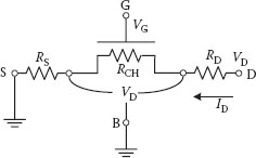
FIGURE 59.1 Equivalent circuit diagram of MOSFET with the source/drain series resistance (RSD) and the channel resistance (RCH).
(59.2) |
where U0 is µ0Cox(WCIR/LEFF) with µ0 denoting low field mobility, COX is the gate oxide capacitance per unit area, WCIR is the circumference of the nanowire, LEFF is the effective gate length, and VD′ is the voltage drop at the intrinsic channel (VD′ ≡ VD I–D RSD). If the θ2 effect is negligible when the device is operating, the Y function is able to be simply modified as
(59.3) |
In a strong inversion regime, VGEFF can be substituted for VG – VTH, and thus the Y function versus the overdrive voltage curve behaves linearly. Fortunately, in NWFET, the linearity of the Y function, indicating little θ2, is observed and it makes the extraction of the RSD process much easier and more accurate. Figure 59.2 shows that the Y function of NWFET is almost linear compared with that of the planar MOSFET resulting from the highly suppressed surface roughness scattering due to the volume inversion effect [19].
As shown in Figure 59.3, the Y function curves of NWFETs with different channel circumferences have linearity indicating that the calculation of parameters such as threshold voltage and low field mobility is accurate for all measured devices with different channel circumferences. The procedure for extracting RSD using the Y function technique is listed as follows:
Step 1. In the first step, the initial value U0 and VTH are extracted from the Y function versus the VG curve in a strong inversion regime, assuming that VD′ is equal to VD. The slope of the Y function curve gives U0, and the x-intercept point of the curve gives VTH (Equation 59.3).
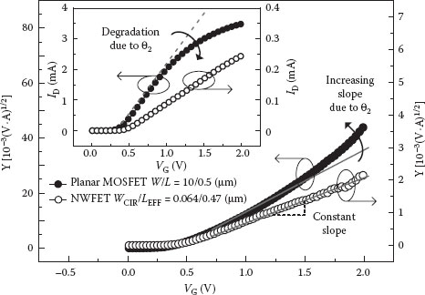
FIGURE 59.2 Measured Y parameter in planar MOSFET and NWFET. The inset shows measured ID in planar MOSFET and NWFET. Lines represent linearly regressed lines.
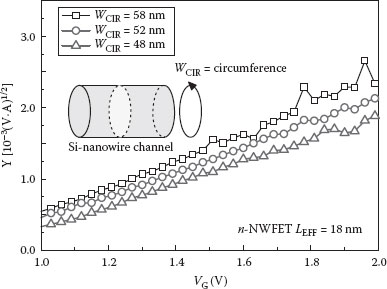
FIGURE 59.3 Y parameter versus VG curves of NWFETs with different channel circumferences (WCIR). Linear dependence on VG was observed in devices with all WCIRs.
Step 2. By using Equation 59.1, U0 and VTH extracted in the previous step are adjusted to the measured ID and gm for a VG range close to VTH and below the VG point at gm.max, where the difference between VD and VD′ is quite small.
Step 3. Once U0 and VTH are extracted, RSD can be fitted to ID and gm for the entire range, including the strong inversion regime.
Step 4. If the root-mean-square error between the measured ID and gm and the simulated ID and gm curve is not the minimal in the subthreshold and strong inversion region, steps 2, 3, and 4 should be performed again after replacing VD by VD′ to extract precise values of U0, VTH, and RSD. This iteration flow ends when the root-mean-square error is smallest among the error values resulting from step 4. The details of the extraction process are exhibited in Ref. [20].
59.2.2 MODELING AND COMPARISON RESULT OF the RSD EXTRACTING PROCEDURE IN NWFET
Figure 59.4 shows that the simulated ID and gm curves with extracted parameters using the Y function technique such as U0, mobility attenuation factors, and RSD are well fitted to the measured curves. The most important factor in Figure 59.4 is the degradation in the ID curve with increasing VG, which is mainly due to the RSD effect. Owing to the complicated junction structure in NWFET, from a one-dimensional source/drain to a three-dimensional channel, the RSD effect is dominant in ID degradation. Also, ID, the degradation caused by the mobility attenuation effect, is almost negligible, and this result has consistency in the linearity of the Y function curve. Again, the volume inversion effect in NWFET, where the carrier moves through the channel forming away from the oxide-to-channel interface, reduces the surface roughness scattering [8,21].
Figure 59.5 shows RSD values normalized in the n- and p-type NWFETs with 48 and 58 nm circumference (WCIR). Because NWFETs have a large dispersion in electrical characteristics, including RSD, the average values of RSD with the same geometry parameter must be examined. In both the 48 and 58 nm WCIR devices, the averaged value of normalized RSD in n-type devices is larger than that in p-type devices. Boron atoms that are implanted into the source/drain region in p-type MOSFET is more diffusive than arsenic, which is used in n-type MOSFET [2,3], and thus it makes the channel-to-source/drain junction, where the RSD value is essentially determined, more ohmic.
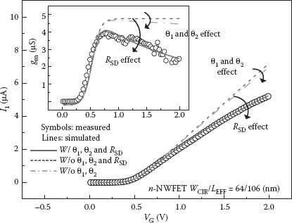
FIGURE 59.4 Measured ID of NWFET (open symbols), simulated ID without the effect of mobility attenuation factors (θ1 and θ2) and RSD (dashed line), simulated ID without the effect of RSD or after considering the effects of θ1 and θ2 only (dash-dotted line), and simulated ID with the effects of θ1, θ2, and RSD (solid line).
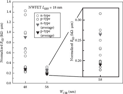
FIGURE 59.5 Extracted RSD values of several NWFETs with different circumferences and doping types.
59.3 INVESTIGATION ON THE C–V CHARACTERISTICS AND EFFECT OF THE BOTTOM PARASITIC TRANSISTOR
59.3.1 DEVICE STRUCTURE AND C–V MEASUREMENT
The capacitance–voltage (C–V) characterization, including gate-to-channel capacitance, includes the essential information of a transistor such as threshold voltage, flatband voltage, inversion charge, and mobility [22,23]. However, C–V characterization in the NWFET has technical issues that need to be investigated in depth due to structural properties. The undoped Si nanowire channel is surrounded by gate material and suspended by the embedded SiGe layer under the source/drain region (refer to Figure 59.6). The structure is built on the Si substrate from which the undoped nanowire channel is electrically floated by a thick dielectric. However, the bottom Si bulk acts as a parasitic transistor with different VTH and mobility from an intrinsic nanowire channel transistor [24] by a gate signal delivered through the SiGe layer. Since the two types of transistors that share the gate and source/drain contribute differently to the charge supply, which determines the capacitance behavior, an extensive study on each capacitance component of the NWFET is needed.
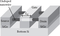
FIGURE 59.6 Schematic of the NWFET with twin Si nanowires. The bottom Si is a p-type substrate and the gate material is TiN, surrounding the intrinsic (undoped) Si nanowire channels. The SiGe layer is embedded under the source/drain region to suspend the nanowire channels.
In this study, the array structure that consists of a 100 × 100 single nanowire capacitor (NWCAP) with WCIR/LG = 64/250 nm was used for experiments as the single device has an extremely scaled active area and is hard to be precisely measured. The detailed fabrication process is reported in Refs. [2,9]. To obtain each capacitance component, various basic configurations were set up; CGSDB represents the capacitance measured with all terminals grounded, CGB represents the capacitance measured with the source/drain floated and body grounded, and CGS denotes the capacitance measured with the body floated and source/drain grounded, respectively. All capacitance values are normalized by the number of nanowires in the array.
59.3.2 GATE SIGNAL RESPONSE OF the INTRINSIC SI NANOWIRE CHANNEL
In this section, the capacitance generation mechanism from component to component is discussed, based mainly upon the descriptions reported in Refs. [12,25].
The total capacitance modulated by a gate signal consists of two components: capacitance from electrons that are injected from the source/drain into the intrinsic Si nanowire channel and capacitance from electrons and holes that are generated at the bottom Si interface. As shown in Figure 59.7, CGB shows a substantial reduction in its value in the strong inversion region (positive VG for an n-type NWFET) compared to CGSDB because the electron injection from the source/drain is eliminated. In such a gate bias region, electrons in the CGB configuration are supplied from the generation in the bottom p-type Si substrate, in which the electrons are minor carriers, showing a frequencydependent behavior. On the other hand, in the accumulation region (negative VG for an n-type NWFET), CGSDB and CGB have almost the same values, indicating that CGB by “fast” hole charging/discharging is most responsible for CGSDB. This interpretation is conceptually illustrated in Figure 59.8. The effect of charging/discharging from the bottom Si only represents the CGB component.
CGSD can be understood in a similar way. Contrary to the CGB, CGSD represents the capacitance component whose charge is supplied solely by the injection from the source/drain into the nanowire channel. In the strong inversion region, CGSD is independent of the frequency as a sufficient number of electrons are injected from the source/drain to follow the gate signal (Figure 59.7). The reason why CGSD shows slightly smaller values than CGSDB is that CGSDB contains a “slow” supply of electrons from the bottom Si. It is important to note, however, that the charging/discharging speed of electrons in the Si channel supplied by the source/drain is much faster than electron generation in the bottom Si. Furthermore, steep VG dependence in CGSD means effective channel inversion and charge supply of the nanowire channel transistor [12]. In the accumulation region, CGSD is much smaller than CGSDB or CGB, resulting from the dominant hole injection from the bottom Si over the hole injection from the source/drain region. It also indicates that the intrinsic nanowire channel has a better off-state gate controllability, thereby suppressing leakage current. This interpretation is illustratively described in Figure 59.8. The effect of charging/discharging from an undoped nanowire channel only represents the CGSD.
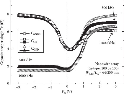
FIGURE 59.7 C–V curves of the n-type NWFET (n-NWFET) with several biasing configurations. Only 1000 kHz data are presented for CGSDB as no frequency dependence was observed in all VG range, indicating that a majority of the carriers (electrons or holes) can be supplied from either source/drain or bottom Si or both at any VG regime. All capacitance values were normalized and represent the value of the single transistor.
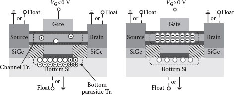
FIGURE 59.8 Illustrative charge distribution in the n-type NWFET with negative and positive VG conditions, respectively. With a corresponding combination of grounded or floated source/drain and body, the charge supply of CGSDB, CGB, and CGSD can be estimated.
As depicted in Figures 59.7 and 59.8, the bottom Si bulk plays a role as another parasitic bottom transistor and has an insignificant effect on the electrical characteristics in the operation region [24]. Still, it is necessary to precisely extract the effect of the bottom parasitic transistor to investigate the intrinsic properties of the Si nanowire channel explicitly, thereby determining the inversion status of the device.
59.3.3 EFFECT OF the SIGE LAYER AND BOTTOM PARASITIC TRANSISTOR IN the SI SUBSTRATE ON C–V CHARACTERISTICS
The SiGe layer is embedded to basically sustain a nanowire channel and improve the electrical characteristics of the p-type NWFET by compressive stress. It is needed to qualitatively investigate the parasitic effect of the bottom Si transistor with the SiGe layer to estimate the exact intrinsic performance of the device. Based on the results in Ref. [26], parasitic capacitance is analyzed with CGSD measurement results with the help of the energy band diagrams. The simulation result is also added to show the effect of conditions in the SiGe layer.
59.3.3.1 Roles of the SiGe Layer in NWFET
In the NWFET structure investigated, owing to the application of the SiGe layer under the source/drain region as a compressive stressor to the nanowire channel, p-type NWFET exhibits greatly enhanced device performance with a slightly degraded n-type NWFET [2]. It was reported that the compressive stress increases as the thickness of SiGe increases, enhancing the hole mobility due to the quantum-confinement-induced suppression in surface scattering [27]. As illustrated in Figure 59.9a, the gate trimming structure of the single devices comprises two different cross sections: A–A′ in Figure 59.9b with the nanowire channel region and B–B′ in Figure 59.9c without the nanowire channel region. In particular, the unexpected electrical leakage path delivering the gate signal to the bottom Si area is formed along B–B′. The contact between the gate and the source/drain causes the SiGe layer to be inverted, resulting in a turn-on of the bottom Si substrate as a parasitic transistor. The parasitic bottom transistor affects the CGSD even though the body is floated. It is thus important to examine the generation mechanism of the parasitic bottom transistor and its capacitance behavior to explicitly extract properties of the intrinsic nanowire transistor and optimize the structure of the nanowire transistor fabricated on the Si Bulk with the SiGe layer embedded.
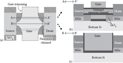
FIGURE 59.9 (a) Top view of the NWFET having two nanowire channels. Owing to the gate trimming process, the device has two different cross sections. (b) A–A′ with the nanowire channel between the source and the drain and (c) B–B′ without the channel. The contact between the gate and the source/drain along B–B′ forms an undesired leakage path delivering the gate signal through the SiGe layer.
59.3.3.2 Analysis of the Turning-On Effect of the Parasitic Bottom Transistor
Figure 59.10 shows the CGSD of the n- and p-NWFET with the parasitic bottom transistor and the nanowire channel transistor depicted, respectively. The effect of the parasitic bottom transistor can be understood using charging/discharging behavior, considering the structural effect in the NWFET with energy band diagrams in Figures 59.11, 59.12, and 59.13, which describe the spatial charge placement in the gate, undoped nanowire channel, and bottom Si substrate at each bias condition. Near VG = 0.2 V, the nanowire channel transistor is turned on so that the electron conduction starts between the source and the drain (Figure 59.11), and this is corresponding to the early steep increase in CGSD in Figure 59.10. The SiGe layer is not inverted enough to provide the electron conduction path through which the gate, source/drain, and bottom Si are connected (Figure 59.12a). Considering the work function of the TiN metal gate, band bending in the SiGe layer and bottom Si substrate is not sufficient yet (Figure 59.12b). However, as VG increases further and reaches 0.9 V, the SiGe is turned on to act as an electron channel, supplying a number of electrons to the bottom Si substrate (Figure 59.13a). The energy band bending in such a bias condition is enough for both the SiGe and the bottom Si region to be strongly inverted (Figure 59.13b). This is responsible for a hump in the CGSD–VG curve in Figure 59.10 (around SiGe turn-on voltage) even though the body is floated. The effect of the parasitic bottom transistor in p-NWFET can be explained in a similar way. The difference from n-NWFET is the value of the turn-on voltage of the SiGe layer. The built-in potential applies as a barrier to an electron in the n-NWFET but helps a hole to be inverted.
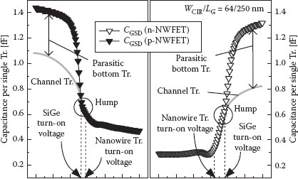
FIGURE 59.10 CGSD versus VG curves of the n-type and p-type NWFET. The hump in the curve corresponds to the SiGe turning-on point and the channel transistor (in thick line) is conceptually drawn to explicitly express the effect of the bottom parasitic transistor.
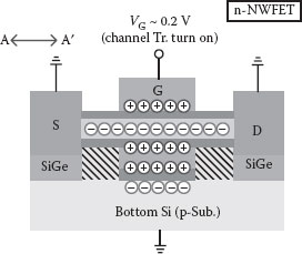
FIGURE 59.11 Charge distribution of the n-type NWFET along A–A′ in the nanowire channel and bottom Si substrate at VG = 0.2 V, which is the Si nanowire channel transistor turn-on point.
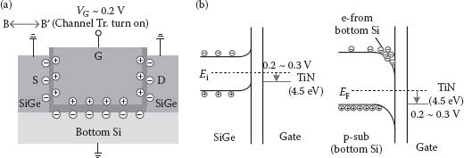
FIGURE 59.12 (a) Charge distribution of the n-type NWFET along B–B′ in the gate and bottom Si substrate at VG = 0.2 V. (b) The SiGe layer and bottom parasitic transistor are not sufficiently biased to be inverted.
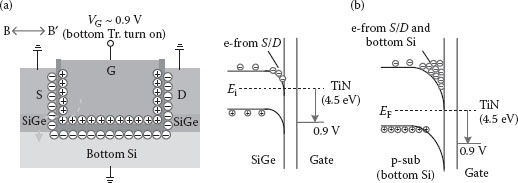
FIGURE 59.13 (a) Charge distribution of the n-type NWFET along B–B′ in the gate and bottom Si substrate at VG = 0.9 V. (b) The SiGe layer and the bottom parasitic transistor are sufficiently biased and strongly inverted. SiGe acts as a channel, a conduction path between the source/drain, gate, and bottom Si transistor so that the electrons from the source/drain are injected to the bottom Si interface area.
The structure of the NWFET includes parasitic components such as series resistance RSD and capacitance in the bottom parasitic transistor. It is important to precisely characterize the parasitic components to evaluate the intrinsic performance of the device.
The Y function technique is known to be helpful in dealing with devices such as the NWFET, which has a large sample-to-sample variation in its electrical characteristics, because this technique enables the RSD to be extracted from the individual device. The Y function technique is valid only if a parameter Y is linearly dependent on VG, which was proved to be true in the NWFETs due to the volume inversion effect and thus suppressed the surface roughness scattering. Furthermore, the parameter Y was also observed to have linearity in devices having different channel circumference WCIR (or effective width). The RSD extraction procedure, where low field mobility, threshold voltage, and effective drain voltage considering the voltage drop across the RSD are iteratively corrected, was proposed as the Y-parameter-based modeling methodology. It was shown that simulated data are successfully fitted to the measured ID and gm data. Most of the degradation in the ID is from the RSD due to the complicated junction structure and quantum effect in the nanowire channel. Also, RSD values were extracted with respect to the doping type. It was found that the RSD of the p-type NWFET are much smaller than that of the n-type NWFET since, with the high diffusivity of boron in the p-well, the channel-to-source/drain junction in the p-type NWFET becomes more ohmic than in the n-type NWFET.
Using various biasing configurations, capacitance components in the NWFET were obtained. The value of each capacitance component and its frequency are dependent on which charging/discharging source, charge injection from the source/drain into the channel, or generation from the bottom Si transistor contributes to the electron/hole supply. It was concluded that in spite of the floated body condition, the bottom parasitic transistor turns on as the VG increases because the SiGe layer is inverted and acts as a leakage path delivering the gate signal to the bottom parasitic transistor. The parasitic transistor affects the inversion status of the NWFET with the intrinsic nanowire channel transistor.
1. S. D. Suk, S.-Y. Lee, S.-M, Kim, E.-J. Yoon, M.-S. Kim, M. Li, C. W. Oh et al., High performance 5 nm radius twin silicon nanowire MOSFET (TSNWFET): Fabrication on bulk Si wafer, characteristics and reliability, in Proc. IEDM Tech. Dig., 2005, pp. 717–720.
2. K. H. Yeo, S. D. Suk, M. Li, Y.-Y. Yeoh, K. H. Cho, K.-H. Hong, S. K. Yun et al., Gate-all-around (GAA) twin silicon nanowire MOSFET (TSNWFET) with 15 nm length gate and 4 nm radius nanowires, in Proc. IEDM Tech. Dig., 2006, pp. 1–4.
3. S. D. Suk, M. Li, Y. Y. Yeoh, K. H. Yeo, K. H. Cho, I. K. Ku, H. Cho et al., Investigation of nanowire size dependency on TSNWFET, in Proc. IEDM Tech. Dig., 2007, pp. 891–894.
4. S. D. Suk, K. H. Yeo, K. H. Cho, M. Li, Y. Y. Yeoh, K.-H. Hong, S.-H. Kim et al., Gate-all-around twin silicon nanowire SONOS memory, in Proc. VLSI Symp. Tech. Dig., 2007, pp. 142–143.
5. S. D. Suk, Y. Y. Yeoh, M. Li, K. H. Yeo, S.-H. Kim, D.-W. Kim, D. Park and W.-S. Lee, TSNWFET for SRAM cell application: Performance variation and process dependency, in Proc. VLSI Symp. Tech. Dig., 2008, pp. 38–39.
6. K. H. Cho, S. D. Suk, Y. Y. Yeoh, M. Li, K. H. Yeo, D.-W. Kim, S. W. Hwang, D. Park, and B.-I. Ryu, Observation of single electron tunneling and ballistic transport in twin silicon nanowire MOSFETs (TSNWFETs) fabricated by top-down CMOS process, in Proc. IEDM Tech. Dig., 2006, pp. 1–4.
7. K. Uchida, J. Koga, R. Ohba, T. Numata, and S. Takagi, Experimental evidences of quantum-mechanical effects on low-field mobility, gate-channel capacitance and threshold voltage of ultrathin body SOI MOSFETs, in Proc. IEDM Tech. Dig., 2001, pp. 633–636.
8. J. Chen, T. Saraya, K. Miyaji, K. Shimizu, and T. Hiramoto, Experimental study of mobility in [110]- and [100]-directed multiple silicon nanowire GAAMOSFETs on (100) SOI, in Proc. VLSI Symp. Tech. Dig., 2008, pp. 32–33.
9. M. Li, K. H. Yeo, S. D. Suk, Y. Y. Yeoh, D.-W. Kim, T. Y. Chung, K. S. Oh, and W.-S. Lee, Sub-10 nm gate-all-around CMOS nanowire transistors on bulk Si Substrate, in Proc. VLSI Symp. Tech. Dig., 2009, pp. 94–95.
10. F. Léonard and A. A. Talin, Size-dependent effects on electrical contacts to nanotubes and nanowires, Phys. Rev. Lett., 97, 026804-1-02684-4, Jul. 2006.
11. R.-H. Baek, C. K. Baek, S. W. Jung, Y. Y. Yeoh, D.-W. Kim, J.-S. Lee, D. M. Kim, and Y.-H. Jeong, Characteristics of the series resistances extracted from Si-nanowire FETs using the Y-function technique, IEEE Trans. Nanotechnol., 9(2), 212–217, Mar. 2010.
12. R.-H. Baek, C.-K. Baek, S.-H. Lee, S. D. Suk, M. Li, Y. Y. Yeoh, K. H. Yeo et al., C-V characteristics in undoped gate-all-around nanowire FET array, IEEE Electron Device Lett., 32(2), 116–118, Feb. 2011.
13. K. K. Ng and W. T. Lynch, The impact of intrinsic series resistance on MOSFET scaling, IEEE Trans. Electron Devices, 34(3), 503–511, Mar. 1987.
14. J. Hu, Y. Liu, C. Z. Ning, R. Dutton, and S.-M. Kang, Fringing field effects on electrical resistivity of semiconductor nanowire-metal contacts, Appl. Phys. Lett., 92, 083503-1-083503-3, Feb. 2008.
15. S. D. Kim, C.-M. Park, and J. C. S. Woo, Advanced model and analysis for series resistance in sub-100 nm CMOS including poly-depletion and overlap doping gradient effect, in Proc. IEDM Tech. Dig., 2000, pp. 723–726.
16. S. Thompson, P. Packan, T. Ghani, M. Stettler, M. Alavi, I. Post, S. Tyagi, S. Ahmed, S. Yang, and M. Bohr, Source/drain extension scaling for 0.1 µm and below channel length MOSFETs, in Proc. VLSI Symp. Tech. Dig., 1998, pp. 132–133.
17. J. Kim, S. Yang, J. Lee, S. D. Suk, K. Seo, D. Park, B.-G. Park, J. D. Lee, and H. Shin, Investigation of mobility in twin silicon nanowire MOSFETs (TSNWFETs), in Proc. Int. Conf. Solid-State Integr. Circuit Technol. (ICSICT), 2008, pp. 50–52.
18. T. Tanaka, Novel parameter extraction method for low field drain current of nano-scaled MOSFETs, in Proc. Int. Conf. Microelectron. Test Struct. (ICMTS), 2007, pp. 265–267.
19. R.-H. Baek, C.-K. Baek, S.-W. Jung, Y. Y. Yeoh, D.-W. Kim, J.-S. Lee, D. M. Kim, and Y.-H. Jeong, Comparison of series resistance and mobility degradation extracted from n- and p-type Si-nanowire field effect transistors using Y-function technique, Jpn. J. Appl. Phys., 49(4), 04DN06–04DN06-5, Apr. 2010.
20. R.-H. Baek, C.-K. Baek, S.-W. Jung, Y. Y. Yeoh, D.-W. Kim, J.-S. Lee, D. M. Kim, and Y.-H. Jeong, Series resistance behavior extracted from silicon nanowire transistors using the Y-function technique, Int. Conf. Solid State Dev. Mater. (SSDM), 2009, pp. 1108–1109.
21. Y.-R. Kim, S.-H. Lee, C.-K. Baek, R.-H. Baek, K.-H. Yeo, D.-W. Kim, J.-S. Lee, and Y.-H. Jeong, Reliable extraction of series resistance in silicon nanowire FETs using Y-function technique, in Proc. Int. Conf. Nanotechnol. Mater. Devices (NMDC), 2011, pp. 262–265.
22. S. Severi, L. Pantisano, E. Augendre, E. San Andrés, P. Eyben, and K. De Meyer, A reliable metric for mobility extraction of short-channel MOSFETs, IEEE Trans. Electron Devices, 54(10), 2690–2698, Oct. 2007.
23. I. Ferain, L. Pantisano, B. J. O’Sullivan, R. Singanamalla, N. Collaert, M. Jurczak, and K. De Meyer, Methodology for flatband voltage measurement in fully depleted floating-body FinFETs, IEEE Trans. Electron Devices, 55(7), 1657–1663, Jul. 2008.
24. S. D. Suk, K. H. Yeo, K. H. Cho, M. Li, Y. Y. Yeoh, S.-Y. Lee, S. M. Kim et al., High-performance twin silicon nanowire MOSFET (TSNWFET) on bulk Si wafer, IEEE Trans. Nanotechnol., 7(2), 181–184, Mar. 2008.
25. Y.-H. Jeong, R.-H. Baek, C.-K. Baek, K. H. Yeo, D.-W. Kim, J. Y. Chung, and D. M. Kim, Comparative study of C-V characteristics in Si-NWFET and MOSFET, in Proc. Int. Conf. Nanotechnol. Mater. Devices (NMDC), 2010, pp. 26–29.
26. R.-H. Baek, M.-D. Ko, S.-H. Lee, C.-K. Baek, K. H. Yeo, D.-W. Kim, J.-S. Lee, and Y.-H. Jeong, Analysis of parasitic bottom capacitance in n- and p-type Si-nanowire field effect transistors on bulk, in Proc. Int. Conf. Nanotechnol., 2011, pp. 139–143.
27. M. Li, K. H. Yeo, Y. Y. Yeoh, S. D. Suk, K. H. Cho, D.-W. Kim, D. Park, and W.-S. Lee, Experimental investigation on superior PMOS performance of uniaxial strained <110> silicon nanowire channel by embedded SiGe source/drain, in Proc. IEDM Tech. Dig.,2007, pp. 899–902.