
Investigations on Nanomagnetic Logic by Experiment-Based Compact Modeling |
CONTENTS
62.4 Nanomagnetic Compact Model
62.5.2 Nanomagnetic 1-Bit Full Adder
Nanomagnetic logic (NML) is an emerging technology using field-coupled nanomagnets that combine logic and memory functionality in a single device [1]. The magnetization state of nonvolatile, bistable nanomagnets is used as a logic state. Digital computation is achieved by magneto-static field-coupling of the nanomagnets. High-density integration due to a scalability of the nanomagnets down to a sub-50 nm size and potential low power consumption for switching of the nanomagnets are key features of NML.
NML with perpendicular magnetic anisotropy (PMA) uses nanomagnets made from, for example, Co/Pt or Co/Ni multilayers and has been proposed in 2002 [2,3]. In contrast to NML with in-plane nanomagnets made of permalloy [4,5], the switching behavior of the out-of-plane nano-magnets is defined by the interface and crystalline anisotropy allowing for a user-defined dot geometry. Additionally, the switching field of the out-of-plane nanomagnets can be controlled by partial focused ion beam (FIB) irradiation [6].
The reversal process of an as-grown nanomagnet is governed by domain wall (DW) nucleation at the weakest spot in the nanomagnet [7]. By applying an external field in the easy-axis direction, the DW nucleates at this weakest link and, after depinning, propagates through the entire dot and completely reverses it [8,9]. The perpendicular magnetic anisotropy of the utilized Co/Pt nano-magnets is achieved by the interface and crystalline anisotropy of the Co and Pt layers [10]. FIB irradiation intermixes the single layers and reduces the switching field of the thin film [11]. Partial FIB irradiation locally reduces the anisotropy in a nanomagnet and therefore creates an artificial nucleation center (ANC) at a user-defined position. The switching behavior of the nanomagnet can be precisely controlled by the size and dose of partial FIB irradiation [6]. For the realization of logic operations, the DW nucleation at the ANC can be supported or constrained by the coupling fields of the surrounding nanomagnets, which superpose with the clocking field and therefore support or inhibit the switching of the dot [12]. The basic building blocks for NML with PMA, such as a majority gate, an inverter chain, or a fanout structure, have already been demonstrated [6,13,14].
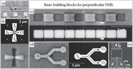
FIGURE 62.1 Basic building blocks for nanomagnetic logic with perpendicular magnetic anisotropy. (a) MFM image of a current wire as electrical input, (b) MFM images of a majority gate for logic operation, (c) MFM images of an inverter chain for signal inversion and transmission, (d) MFM images of a fanout to split magnetic signals, and (e) SEM image of a Hall sensor as electrical output.
In a majority gate with PMA (Figure 62.1b), the superposing coupling fields of the input dots I1, I2, and I3 stabilize or destabilize the magnetization state of the output O during clocking and therefore force or inhibit its switching. Owing to the antiparallel orientation of the coupling fields from a nanomagnet, compared to its own magnetization state, the output O is always aligned antiparallel compared to the input majority [13]. In an inverter chain (Figure 62.1c), magnetic signals are transmitted over two dots per clocking cycle. During clocking, consecutive nanodots with the same magnetization state as their prior neighbors are destabilized by its coupling field and therefore forced to switch to the antiparallel state [14]. A fanout structure (Figure 62.1d) can be realized by cloning a propagating domain wall from the input I1 to two (or more) output wires O1 and O2 [6].
Perpendicular NML uses alternating, homogeneous magnetic fields in an easy-axis direction for clocking [14], which can be generated by either external or integrated coils. On-chip inductors operating up to 100 MHz have been shown in Ref. [15], but they have to be modified for the implementation of NML. Alternative clocking concepts using the magnetic stray field of a propagating DW as a clocking field are currently under investigation [16].
Integration in standard CMOS circuits can be achieved by electrical input and output structures. Current wires generating oersted fields (Figure 62.1a) as input structures or Hall sensors in the split-current design (Figure 62.1e) to read out the magnetization state of a nanodot are standard I/O devices for magnetic systems [17,18]. Increased sensitivity can be achieved by GMR and MTJ structures. Those devices are standard CMOS-compatible structures to set or read out the magnetization state of sub-100 nm nanodots with perpendicular magnetic anisotropy [19,20].
Micromagnetic simulations like object-oriented micromagnetic framework OOMMF [21] are widely used for simulations and investigations on magnetic structures. Such micromagnetic modeling tools are highly accurate but also very time intensive and therefore not capable of simulating large NML circuits. Hence, simplified physical dot models that accurately mimic the behavior of the nanomagnets are needed. In this chapter, an experiment-based compact model for NML with PMA is presented. Compact modeling of the switching and the interaction of the nanomagnets allows for fast and accurate predictions on the behavior of complex NML circuits [22].
Figure 62.2 shows the simplified physical model for the nanomagnets. The switching behavior of the single-domain nanomagnets is described by the switching field Hc (Figure 62.2a). Once the applied external field Hext reaches the switching field, a DW is nucleated at the weakest spot and propagates through the entire dot to switch its magnetization M.
Interaction of the nanomagnets is achieved by their magnetic stray field, often named as the coupling field k, which superposes with the external field Hext on a neighboring nanomagnet (62.2b).
Hence, nanomagnets with parallel magnetization destabilize each other and the switching field Hc is reduced by the coupling field k to Hp→ap. Once one of the dots switches, the nanomagnets are in the stabilizing, antiparallel magnetization state. Hence, the switching field Hc of the second dot to switch it in the parallel state is increased by k to Hap→p.
An applied, sinusoidal clocking field with adequate amplitude Hclock will force parallel magnetized dots in the antiparallel state without affecting the magnetization of antiparallel ordered dots. Owing to the influence of fabrication variations, the switching field is not constant from dot to dot and is described by a switching field distribution (SFD) [23]. Additionally, the nanomagnets underlie the influence of thermal noise, which causes an additional SFD for each dot [24]. Both SFDs convolute to an effective SFD with standard deviation σeff, which narrows the clocking window from the former two times the coupling strength [14]. For the correct operation of the perpendicular NML circuits, the coupling fields of the nanomagnets have to overcome the effective SFD to keep up the clocking window.
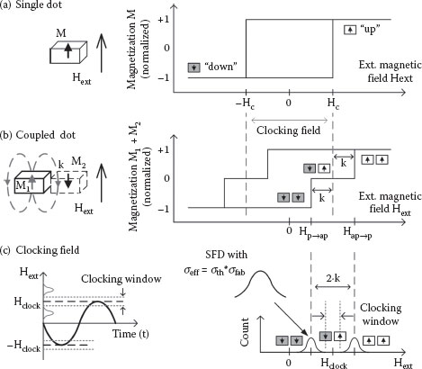
FIGURE 62.2 Simplified model of field-coupled nanomagnets. The switching behavior of the single-domain nanomagnets is described by the switching field Hc (a). The coupling field k of a neighboring nanomagnet superposes with the external field Hext and therefore reduces the switching field to the antiparallel state to Hp→ap by the strength of the coupling field k (b). The switching field distribution of the nanomagnets caused by fabrication variations and thermal noise reduces the clocking window (c).
The Pt5 nm[Co0.4 nmPt1.0 nm]×8Pt3 nm multilayer stack is magnetron sputtered on a thermally oxidized Si <100> wafer. The 5 nm Pt seed layer prefers the (111) growth that is required to generate the perpendicular anisotropy of the Co layers [25]. The 3 nm Pt top layer prevents the Co layers from oxidation. The nanomagnets are fabricated by FIB lithography using a PMMA photoresist and an evaporated Ti hard mask. After ion beam etching, the nanomagnets are partially irradiated using a 50 kV Ga+ FIB system. In the following, the switching behavior of the nanomagnets will be analyzed by magneto-optical microscopy.
The switching field Hc of a single magnet varies over time due to thermal noise and may be described by an Arrhenius-type model [24,26]. Figure 62.3 shows the thermally induced SFD of a 1 µm∙1 µm dot. In a first approximation, the influence of thermal noise can be modeled by a Gaussian distribution with mean mn = Hc and standard deviation (SD) σn. Comparisons between measurements and the following simulations show that modeling of thermal noise by a Gaussian distribution is justified. For our sample, we measured a thermally induced SFD with an SD of σn = 3 mT.
Owing to fabrication variations, the switching field Hc also varies from dot to dot [23]. The origin of those variations can be traced back to edge roughness, edge oxidation, and grain formations occurring during the sputter process [7]. By partial FIB irradiation of the nanomagnets, the intrinsic switching field distribution (SFD) is rendered ineffective and replaced by the distribution caused by the ANCs [6]. Figure 62.4 shows the measurement results for the switching field Hc, depending on the irradiation dose for a 10 nm∙10 nm and 20 nm∙20 nm irradiation area. The coercivity Hc remains constant at approximately masgrown ≈ 400 mT below a certain dose, depending on the irradiation size. For higher doses, the coercivity drops below the DW nucleation and depinning limit at the ANC and then remains constant again at roughly mANC ≈ 100 mT. Fortunately, the absolute SFD of the ANCs is considerable smaller than the intrinsic SFD. The SD is reduced from σasgrown = 25 mT to σANC = 6.5 mT for the irradiated dots at high doses.
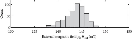
FIGURE 62.3 Thermally induced switching field distribution of a single nanomagnet with 1 µm⋅1 µm size.
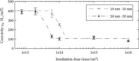
FIGURE 62.4 Switching field Hc of Co/Pt nanomagnets depending on the dose and size of the partial irradiation. The intrinsic switching field distribution of the nanomagnets is replaced by the distribution of the artificial nucleation centers. Both the mean and standard deviation of the coercivity are significantly reduced.
Summing up, the switching field Hc of a nanomagnet can be generally described by
(62.1) |
with normally distributed random variables zHc, Zn (t) ∈ 1 (0, 1). As discussed before, partial FIB irradiation creates artificial nucleation centers and replaces the intrinsic SFD by one of the partially irradiated nanomagnets with ANC:
(62.2) |
Previous experiments showed that the switching field Hc,pi has to be lower than the intrinsic switching field Hc by two times the coupling field k to achieve directed signal flow in a wire [27]:
(62.3) |
The interaction between two dots is described by the coupling field k caused by the magnetic stray field of the nanomagnets. In a first approximation, it can be calculated by finite element simulations using the point-dipole approximation [2].
Here, the nanomagnet is divided into small finite elements of roughly 10 nm∙10 nm∙10 nm size. The dipole field of each element is then calculated by
(62.4) |
with being the vector to the point of interest, r the absolute value of the unit vector in the direction of , the dipole moment of each element, and the three-dimensional delta function. The dipole moment can be calculated by
(62.5) |
with Ms being the saturation magnetization of the utilized multilayer, dx∙dy∙dz the size of each element, and the unit vector with the direction of the nanomagnet magnetization. The coupling field of the complete nanomagnet can then be calculated by the superposition of the dipole field of each element.
Figure 62.5 shows the simulation results of the coupling field k of a 400 nm∙400 nm dot with eight multilayers (ML) of 0.4 nm Co each. The coupling field drops with 1/dn over the distance d from the border of the nanomagnet with 1 < n < 3, depending on the geometry of the nanomagnet (squared dot: n ≈ 1). The strength of the coupling field on the subsequent nanomagnet depends not on the distance between the dots but on the effective distance to its DW nucleation center, which is considerably larger [14]. In an experiment with coupled 800 nm∙800 nm dots, we observed a coupling field of k = 4.5 ± 1.1 mT for an interdot distance of d = 100 nm. The results coincide with the simulation results, where the SD σk can be traced back to variations on the distance between the nanomagnet and the ANC of the subsequent dot. Hence, an additional standard deviation σk due to fabrication variations in the shape and edge roughness is taken into account.
Summing up again, the coupling field k of the nanomagnets can be modeled by
(62.6) |
where mk is calculated using the point-dipole approximation described above and Zk ∈ N (0, 1).
The coupling field may be enhanced by increasing the number of multilayers, but a reduction in the natural domain size and, therefore, the maximal size of the nanomagnets has to be taken into account. Another way to enhance the coupling field is to adapt the shape of the nanomagnets that is not limited due to the interface anisotropy of the Co/Pt multilayer film. The stray field of a nanomagnet with an optimized geometry is concentrated at one spot, where the ANC of the subsequent nanomagnet can be located. Figure 62.6 shows the simulation results for the coupling fields of an optimized inverter structure (a) and a majority gate (b). The stray field of the fork-like inverter structure is concentrated right in the gap between both arms, in which the ANC of the following dot (marked as dashed line) is placed. Measurements on such inverter structures show coupling fields in the 15 mT range, which is sufficient for the realization of complex NML circuits. Both the measurements and simulations on the majority gate resulted in coupling fields of ≈5 mT for each input magnet.
Further simulations show that a misalignment of the ANC would degrade the functionality of the majority gate due to the rapid decay of the coupling fields over a distance. A misalignment by several nanometers in one direction would increase the influence of one input and, at the same time, decrease the influence of the others [13]. A variance on the alignment of the ANC due to fabrication variations is considered during the calculation of the coupling fields of each nanomagnet and results in correlated inequalities of the coupling fields in a majority gate.
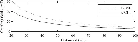
FIGURE 62.5 Simulation results for the coupling field k depending on the distance d from the edge of a 400 nm ⋅ 400 nm nanomagnet and the number of multilayers (ML) of the utilized Co/Pt film.
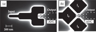
FIGURE 62.6 Simulation results for the coupling fields of an optimized structure for an inverter structure (a) and a majority gate (b). The nanomagnets are marked as a black area; the white color indicates field strengths of at least 20 mT. The shape of the input magnets concentrates the coupling fields on the position of the ANC of the subsequent nanomagnet (indicated as a dashed line).
62.4 NANOMAGNETIC COMPACT MODEL
The analyzed switching behavior of the nanomagnets and the coupling field calculated by the point-dipole approximation are now implemented in the compact models. Figure 62.7 shows the simulation model and the corresponding technological implementation of an inverter and a majority gate.
In our model, the coupling fields of each nanomagnet on the subsequent dot are calculated with respect to the exact geometry of the nanomagnets and the location of the ANC. Each dot can be described to have the switching field Hc,pi caused by the ANC. Once the irradiated part of the dot switches, the whole dot gets reversed by a propagating domain wall.
Figure 62.8 shows the block diagram of the implemented model of an output dot in a majority gate. The magnetization states M1, M2, and M3 of the input dots I1, I2, and I3 with Mi = ±1 are multiplied by the strength of their coupling field k. Owing to the antiparallel impact of the coupling field compared to the input’s own magnetization state, the coupling fields are subtracted from the external clocking field Hext. The hysteresis of the nanomagnet is modeled by the switching field Hc,pi. Once the sum of the coupling and clocking fields reaches the switching field, the nanomagnet switches its magnetization state Mout = ±1. The switching delay models the time needed to propagate the DW through the entire dot.
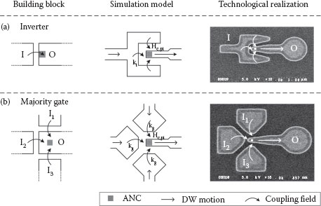
FIGURE 62.7 Compact models used for the simulation and technological realization of an inverter (a) and a majority gate (b).
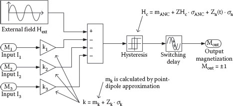
FIGURE 62.8 Block diagram of the implemented model of an output dot in a majority gate.
The presented compact models are now compared to experiments to validate the accuracy of the model. First, the simulation of the thermally induced SFD of a single dot is compared to the experimental results (Figure 62.9). In both experiments and simulations, 500 hysteresis curves of a single, uncoupled dot are performed and analyzed in 1 mT steps to extract the switching events of each curve. The simulation has been performed with a time-dependent, Gaussian distributed switching field Hc,pi with σn = 3 mT. The simulation results are in very good agreement with the experiment and therefore confirm the assumption of a Gaussian distributed thermal noise of the switching field.
To verify the simulated interaction between the dots, a coupled pair with an input dot D1 and a partially irradiated dot D2 are both measured and simulated. The size of the dots is 1 µm∙1 µm with an interdot distance of d = 100 nm. Depending on the magnetization of the input dot D1, its coupling field supports or counteracts the switching of the nanomagnet D2. Hence, the thermally induced SFD of D2 is shifted depending on the input dot magnetization. Figure 62.10 shows the corresponding SFDs of both the measurement and simulation results. 200 hysteresis curves for each of the input configurations D1↓ and D1↑ were both measured and simulated and afterward analyzed in 1 mT steps to identify the SFDs. The distance between the two peaks of the SFDs is μ0∙ΔHc,mean =2⋅k = 10 mT for both measurements and simulations. The results are in very good agreement, verifying the calculation of the coupling field by the presented point-dipole approximation.
Summing up, the comparison between measurements and simulations demonstrates the validity and accuracy of the presented compact models.
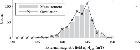
FIGURE 62.9 Comparison between measurement and simulation of the thermally induced switching field distribution of a single nanomagnet.
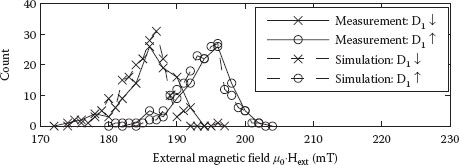
FIGURE 62.10 Comparison between measurement and simulation of the switching behavior of a partially irradiated, coupled nanomagnet. Owing to the influence of the coupling field of its neighbor D1, the thermally induced switching field distribution of D2 is shifted to the left (D1↓) and the right (D1↑).
62.5.2 NANOMAGNETIC 1-BIT FULL ADDER
For investigations on a complex NML circuit, simulations were performed on a 1-bit full adder (Figure 62.11). The structure only consists of 12 nanomagnets arranged in three majority gates (G1, G2, and G3) and four inverters, demonstrating the great benefit of the majority decision. The input magnets are A (with A = A1 = A2), B (with B = B1 = B2), and the carry-in Cin. The sum S and the carry-out Cout are the output magnets. The width of the nanomagnets is 200 nm and the gap between the nanomagnets is d = 50 nm.
The structure is clocked using a homogeneous, external clocking field. The input magnets are not partially irradiated and therefore set prior to the simulation. With random initial states of all nano-magnets and with respect to the longest path, the correct logic computation of the output magnets (complete antiparallel ordering of the nanomagnets) is achieved during five clocking cycles in the worst case scenario.
For simulations on the error rate e of the full adder, the total amount of Cobalt tCo of the utilized multilayer and the fabrication-dependent standard deviation of the switching field σANC are varied.
The standard deviation of the thermal noise has been set to σn = 3 mT, the SD of the coupling field to σk = 0.5 mT, and the SD of the ANC alignment to σalign = 10 nm. Monte Carlo simulations with a total of 35,000 simulations were performed to investigate the parameter-dependent error rate of the full adder. An error is counted if the nanomagnets of the full adder are not in the correct order after a maximum of five clocking cycles. Simulation results are shown in Figure 62.12.
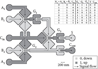
FIGURE 62.11 Simulation model of a 1-bit full adder in perpendicular NML.
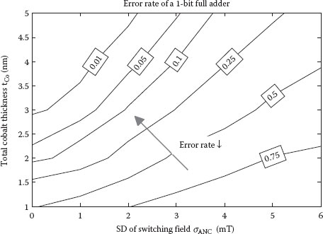
FIGURE 62.12 Error rate e of a 1-bit full adder depending on the total amount of cobalt tCo of the utilized multilayer and the fabrication-dependent standard deviation of the switching field σANC.
As a result, the error rate strongly depends on the switching field variations and the total amount of cobalt, which corresponds to an almost linear increase of the coupling field. This shows the importance of small fabrication variations and at the same time strong dipolar coupling for accurate computing devices and systems realized with perpendicular NML.
Higher coupling fields can be achieved by small distances between the field-coupled nanomagnets in the order of 20–30 nm. Additionally, the total amount of cobalt in the utilized multilayer system can be increased to enhance the magnetic moment. Smaller variations can be reached by optimization on partial irradiation. A reduction of both the mean and SD of the nucleation and depinning fields at the ANC may be achieved by a smooth anisotropy gradient from the ANC to the unirradiated area of the nanomagnet [28].
Nanomagnetic logic with perpendicular magnetic anisotropy uses field-coupled nanomagnets and homogeneous clocking fields for the implementation of logic circuits. A partially focused ion beam irradiation is used to create artificial nucleation centers to realize directed signal flow and logic computation in an array of field-coupled nanomagnets. Coupling fields are superposed with the external clocking field and therefore enforce or inhibit the switching of the nanomagnets.
Experiments show that the switching field Hc,pi of partially irradiated nanomagnets can be described by a Gaussian distribution with mANC ± σANC, which strongly depends on the size and dose of the partial irradiation. Additionally, a time-dependent Gaussian distribution (σANC) caused by thermal noise has to be taken into account. The coupling field k between the nanomagnets can be calculated using the point-dipole approximation considering the saturation magnetization Ms of the utilized multilayer, the geometry of the nanomagnets, and the location of the ANC of the subsequent dot.
Comparisons to experiments on single and coupled nanomagnets demonstrate the accuracy of the described model of the nanomagnets. Further simulations on the error rate of a 1-bit full adder demonstrate the great benefit of the compact models, which allow for fast and accurate investigations on the behavior of complex NML circuits.
Potential applications for NML are memory intensive, low-power applications, where robustness, synchronicity, and parallel pipelined computing is more important than extremely high speed. Owing to the compatibility of NML to CMOS technology, hybrid CMOS/NML circuits utilizing I/O structures like GMRs or MTJs are feasible. The scalability of the nanomagnets has been proven to be less than 50 nm. Hence, a programmable NAND/NOR gate would fit in an area of 200 nm∙200 nm, which is comparable to CMOS in a 22 nm technology. The speed of NML circuits is limited by the propagation speed of the domain walls (10–100 m/s), the size of the nanomagnets, and the frequency of the clocking field (up to 100 MHz with integrated coils). Regarding the power consumption during the clocking of perpendicular NML, low DW nucleation and depinning fields at the ANCs as well as small DW propagation fields in the unirradiated area of the nanomagnets are essential. In patterned Co/Pt nanomagnets, the field needed for the DW propagation is significantly lower than that needed for the DW nucleation and depinning [29]. Measurement results of Ref. [28] show that by an anisotropy gradient the pinning of the DW may be decreased and the coercivity can be reduced below 10 mT. Co/Ni multilayers are a promising candidate to further reduce both the DW nucleation and propagation fields to the low mT range [30].
1. The International Technology Roadmap for Semiconductors: Emerging Research Devices (ERD), 2011. [Online]. Available at: http://www.itrs.net/Links/2011ITRS/2011Chapters/2011ERD.pdf.
2. G. Csaba, A. Imre, G. H. Bernstein, W. Porod, and V. Metlushko, Nanocomputing by field-coupled nano-magnets, IEEE Transactions on Nanotechnology, 1(4), 209–213, 2002.
3. M. Becherer, G. Csaba, R. Emling, W. Porod, P. Lugli, and D. Schmitt-Landsiedel, Field-coupled nano-magnets for interconnect-free nonvolatile computing, Digest Technical Papers IEEE International Solid-State Circuits Conference (ISSCC), pp. 474–475, 2009.
4. A. Imre, G. Csaba, L. Ji, A. Orlov, G. Bernstein, and W. Porod, Majority logic gate for magnetic quantum-dot cellular automata, Science, 311, 205–208, 2006.
5. E. Varga, G. Csaba, G. H. Bernstein, and W. Porod, Implementation of a nanomagnetic full adder circuit, Proceedings of the 11th IEEE Conference on Nanotechnology (IEEE-NANO), pp. 1244–1247, 2011.
6. S. Breitkreutz, J. Kiermaier, V. K. Sankar, G. Csaba, D. Schmitt-Landsiedel, and M. Becherer, Controlled reversal of Co/Pt dots for nanomagnetic logic applications, Journal of Applied Physics, 111, 07A715, 2012.
7. J. W. Lau, R. D. McMichael, S. H. Chung, J. O. Rantschler, V. Parekh, and D. Litvinov, Microstructural origin of switching field distribution in patterned Co/Pd multilayer nanodots, Applied Physics Letters, 92, 012506, 2008.
8. J. Pommier, P. Meyer, G. Pénissard, J. Ferré, P. Bruno, and D. Renard, Magnetization reversal in ultrathin ferromagnetic films with perpendicular anisotropy: Domain observations, Physical Review Letters, 65(16), 2054–2058, 1990.
9. G. Hu, T. Thomson, C. T. Rettner, and B. D. Terris, Rotation and wall propagation in multidomain Co/Pd islands, IEEE Transactions on Magnetics, 41, 3589–3591, 2005.
10. W. B. Zeper, H. W. van Kesteren, B. A. J. Jacobs, J. H. M. Spruit, and P. F. Carcia, Hysteresis, microstructure, and magneto-optical recording in Co/Pt and Co/Pd multilayers, Journal of Applied Physics, 70, 2264–2271, 1991.
11. C. Vieu, J. Gierak, H. Launois, T. Aign, P. Meyer, J. P. Jamet, J. Ferré et al., Modifications of magnetic properties of Pt/Co/Pt thin layers by focused gallium ion beam irradiation, Journal of Applied Physics, 91(5), 3103–3110, 2002.
12. S. Breitkreutz, J. Kiermaier, X. Ju, G. Csaba, D. Schmitt-Landsiedel, and M. Becherer, Nanomagnetic logic: Demonstration of directed signal flow for field-coupled computing devices, IEEE Proceedings of the 41st European Solid-State Device Research Conference ESSDERC, pp. 323–326, 2011.
13. S. Breitkreutz, J. Kiermaier, I. Eichwald, X. Ju, G. Csaba, D. Schmitt-Landsiedel, and M. Becherer, Majority gate for nanomagnetic logic with perpendicular magnetic anisotropy IEEE Transactions on Magnetics, 48, 4336–4339, 2012.
14. I. Eichwald, J. Kiermaier, S. Breitkreutz, G. Csaba, D. Schmitt-Landsiedel, and M. Becherer, Nanomagnetic logic: Error-free, directed signal transmission by an inverter chain IEEE Transactions on Magnetics, 48, 4332–4335, 2012.
15. D. Gardner, G. Schrom, F. Paillet, B. Jamieson, T. Karnik, and S. Borkar, Review of on-chip inductor structures with magnetic films, IEEE Transactions on Magnetics, 45(10), 4760–4766, 2009.
16. G. Csaba, J. Kiermaier, M. Becherer, S. Breitkreutz, X. Ju, P. Lugli, D. Schmitt-Landsiedel, and W. Porod, Clocking magnetic field-coupled devices by domain walls, Journal of Applied Physics, 111, 07E337, 2012.
17. J. Kiermaier, S. Breitkreutz, G. Csaba, D. Schmitt-Landsiedel, and M. Becherer, Electrical input structures for nanomagnetic logic devices, Journal of Applied Physics, 111, 07E341, 2012.
18. J. Kiermaier, S. Breitkreutz, X. Ju, G. Csaba, D. Schmitt-Landsiedel, and M. Becherer, Field-coupled computing: Investigating the properties of ferromagnetic nanodots, Solid-State Electronics, 65–66, 240–245, 2011.
19. D. Ravelosona, S. Mangin, Y. Lemaho, J. A. Katine, B. D. Terris, and E. E. Fullerton, Domain wall creation in nanostructures driven by a spin-polarized current, Physical Review Letters, 96, 186604, 2006.
20. S. Mangin, D. Ravelosona, J. A. Katine, M. J. Carey, B. D. Terris, and E. E. Fullerton, Current-induced magnetization reversal in nanopillars with perpendicular anisotropy, Nature Materials, 5, 210–215, 2006.
21. http://math.nist.gov/oommf/.
22. S. Breitkreutz, J. Kiermaier, C. Yilmaz, X. Ju, G. Csaba, M. Becherer, and D. Schmitt-Landsiedel, Nanomagnetic logic: Investigations on field-coupled computing devices by experiment-based compact modeling, Proceedings of the 11th IEEE International Conference on Nanotechnology (IEEE-NANO), pp. 1248–1251, 2011.
23. T. Thomson, G. Hu, and B. D. Terris, Intrinsic distribution of magnetic anisotropy in thin films probed by patterned nanostructures, Physical Review Letters, 96(25), 257204, 2006.
24. J. B. C. Engelen, M. Delalande, A. J. le Febre, T. Bolhuis, T. Shimatsu, N. Kikuchi, L. Abelmann, and J. C. Lodder, Thermally induced switching field distribution of a single CoPt dot in a large array, Nanotechnology, 21, 035703, 2010.
25. C. L. Canedy, X. W. Li, and Gang Xiao, Large magnetic moment enhancement and extraordinary Hall effect in Co/Pt superlattices, Physical Review B, 62, 508–519, 2000.
26. H.-T. Wang, S. T. Chui, A. Oriade, and J. Shi, Temperature dependence of the fluctuation of the switching field in small magnetic structures, Physical Review, 69, 064417, 2004.
27. S. Breitkreutz, J. Kiermaier, C. Yilmaz, X. Ju, G. Csaba, D. Schmitt-Landsiedel, and M. Becherer, Nanomagnetic logic: Compact modeling of field-coupled computing devices for system investigations, Journal of Computational Electronics, 10, 352–359, 2011.
28. J. H. Franken, M. Hoeijmakers, R. Lavrijsen, J. T. Kohlhepp, H. J. M. Swagten, B. Koopmans, E. van Veldhoven, and D. J. Maas, Precise control of domain wall injection and pinning using helium and gallium focused ion beams, Journal of Applied Physics, 109, 07D504, 2011.
29. M. Delalande, J. de Vries, L. Abelmann, and J. C. Lodder, Measurement of the nucleation and domain depinning field in a single Co/Pt multilayer dot by anomalous Hall effect, Journal of Magnetism and Magnetic Materials, 324, 1277–1280, 2012.
30. D. Stanescu, D. Ravelosona, V. Mathet, C. Chappert, Y. Samson, C. Beigne, N. Vernier, J. Ferre, J. Gierak, E. Bouhris, and E. E. Fullerton, Tailoring magnetism in CoNi films with perpendicular anisotropy by ion irradiation, Journal of Applied Physics, 103, 07B529, 2008.