
Parallel Energy Minimizing Computation via Dipolar Coupled Single Domain Nanomagnets |
CONTENTS
63.2 Field-Coupled Computational Technologies
63.3 Application: Digital Media Object Detection
63.4 Correspondence between Vision and Magnets
At the onset of the twenty-first century, we are presented with stimulating prospects to develop technologies capitalizing on the reduction of feature sizes to produce unique behaviors. The term nanotechnology is often used loosely, but a well-accepted definition is technology that advantageously uses phenomena occurring at critical features of approximately 1–100 nm [1,2]. Particularly for current computational technologies, this creates challenges to overcome, but also provides opportunities to explore novel paradigms and unconventional implementations of logic and memories.
Traditional complementary metal-oxide-semiconductor (CMOS) devices began to feel the concluding “squeeze” of Moore’s law when the transistor’s critical dimension, the gate length, approached sub-100 nm around 2002 known as the 90 nm node. To mitigate various detrimental effects in microprocessor units, several new strategies were introduced, such as high-k gate dielectrics, strained silicon, and more recently, the use of a three-dimensional Tri-gate structure which can be found commercially in Intels 22 nm node Ivy Bridge processors [3,4]. By 2013, the doubling of device density will cease to trend every 2 years and move to a 3-year cycle [5]. With optimistic scaling predictions of CMOS gate lengths to approximately 6 nm and the aforementioned conclusion of Moore’s law, alternative logic paradigms are on the forefront of exploration.
There have been recent proposals for the use of nanomagnets to directly solve quadratic minimization problems, especially those arising in computer vision applications. This is unlike proposals for using nanomagnets to represent binary states. A collection of nanomagnets, when driven to their ground states, can be seen to optimize a quadratic energy function that is determined by their relative placement. By controlling the relative placement of nanomagnets, we can change the energy function being minimized. In this work, we experimentally demonstrate this capability by fabricating and testing an example of a quadratic optimization problem that accomplishes line grouping.
63.2 FIELD-COUPLED COMPUTATIONAL TECHNOLOGIES
There has been a significant growth of interest in field-coupled computing as a radically different computing paradigm. The customary way for charge-based switches, such as a CMOS transistor, to propagate information is through the displacement of charge over a physical connection. The dilemma with this architecture is that once it reaches a critical dimension, classical mechanics makes way for effects like quantum tunneling and the device is no longer operational. Field-based computing is distinctive in that devices are no longer physically connected but still communicate through force fields and may also rely on effects such as quantum tunneling. One such architecture that has been proposed is cellular automata [6,7]. Cellular automata architectures are based on cells where electrons tunnel from one redox site, abstracted in Figure 63.1, to another and interact with neighboring cells through Coulombic forces (quantum dot cellular automata) [8, 9, 10 and 11].
Another possibility is to use magnetic coupling. This is particularly attractive since this form of computing can be implemented at room temperatures [12], unlike those based on electronic charge interactions, which require very low temperatures. Bandhyopadhay [13] has advocated the use of local spin coupling for computing, a middle ground between quantum computing and spintronic transistors. The architecture is essentially a cellular automata architecture, but with spin coupling energies for logic computing. So far, suggestions for field-coupled computing have been made for Boolean logic-based computing [7,12]. Indeed, most work on nanologic seeks to replicate traditional computing involving logic and arithmetic operations [14, 15 and 16]. Other applications that have been proposed with QCAs are signal processing [17], permutation matrices [18], interconnection networks [19], and fast Fourier transforms [20]. However, the energy minimization aspects of CAs have not been directly harnessed [21]. Since nanodevices are expected to have high error rates, both fabrication related and during operations, it makes sense to consider error-tolerant applications where the cost of failure of not finding the optimal solution is not high; even solutions that are close to optimal ones suffice in practice. One such context is in quadratic optimization that arises in computer vision. Energy minimization plays a central role in computer vision algorithms. Nanomagnets offer a tantalizing alternative to traditional form of digital computing for solving quadratic energy minimization problems, drastically reducing the computational time required. Collection of nanomagnets, when driven to their ground states, can be seen to optimize a quadratic energy function that is determined by their relative placement. By controlling the relative placement of magnets, we can change the energy function being minimized. It is somewhat like analog computing from the past, except that instead of solving differential equations, we solve minimization problems.
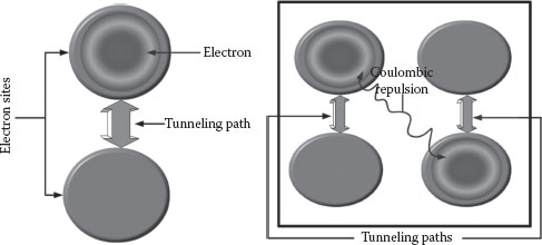
FIGURE 63.1 An abstraction of a quantum-dot cellular automata cell. The electrons tunnel from one site to another and configure themselves in the lowest possible energy state. Similarly, placing cells sufficiently close to one another would induce inter-cell coupling via Coulombic interactions, allowing for more complex functionality.
63.3 APPLICATION: DIGITAL MEDIA OBJECT DETECTION
Imagine an energy minimization co-processor based on nanomagnets that are heterogeneously integrated with CMOS. In the long term, these vision computing circuits can be integrated with camera circuitry to design cognitive cameras, capable of higher level reasoning. The “complier” for this form of computing would transform a given energy minimization problem into a set of equivalent coordinates for a magnet collection. These magnets would be “selected” from a regular grid of nanomagnets by driving the noncomputing magnets into noninteracting vortex states. The array would then be clocked to its ground state. The final states would be read off as the solution to the problem. The vision problem would then use these magnetic measurements as the solution. We will essentially be solving an optimization problem with each input-and-read-out cycle as compared to orders of magnitude more clock cycles that would be needed in a Boolean logic circuit. The current work is toward this long-term goal. We experimentally demonstrate the viability of using single domain nanomagnetic coupling for function minimization computing. Unlike logic and arithmetic computing tasks that demand exact computations, vision problems can work with near-optimal solutions. These vision problems place high demand on computational resources (on Boolean logic-based computing platforms). There have been proposals for using regular arrays of quantum dots [22,23] and nanomagnets [24] for low-level vision, mainly segmentation where the input and the output are both regular grid of pixels. In this chapter, we consider quadratic energy forms that arise in contexts involving extended image features rather than individual pixels. These problems have high-computational complexity and are not amenable to single-instruction-multiple-data (SIMD)-type hardware solutions. To solve the vision problems that we target, VLSI implementation using traditional logic would require complex multiple-instruction-multiple-data (MIMD) architectures as opposed to just SIMD architectures, which are prevalent in the design of vision chips [25]. For instance, a recent proposal for an object recognition chip uses both SIMD and MIMD components [26].
The detection of significant features in an image is a computationally expensive process. The term perceptual organization is used to describe the act of recognizing important features of an image. It is commonly broken down into three steps:
• Segmentation-extraction of features from an image such as edges, textures, pixel intensity, and so on.
• Grouping-relating low-level segments of an image into larger perceptual groups such as surfaces, background, foreground, and so on.
• Recognition-matching groupings identified as significant to a known model such as a building, human, and so on.
Although each step has its own associated complexities, grouping is specifically important when reducing computational intensity. The grouping of low-level segments can be accomplished through a quadratic energy maximization process [24]. Traditional Boolean architectures found in supercomputers normally reduce problems such as the optimization of quadratic problems into finding exact solutions of arithmetic problems and logical operations. This can be very demanding on a Boolean system and is not necessarily required for the grouping of visual objects, and magnetic nano-systems present a unique way to accomplish such a task. For instance, in Figure 63.3a, the task is to find the visually salient or important edges, such as the 3 parallel lines in the center of the image. The grouping of these lines does not require exact computational accuracy, meaning that solutions that are near the optimal result are acceptable [27,28].
Let there be N straight lines in the image that we would like to group. With each straight line, let us associate a variable, xi, taking on values 1 or 0, denoting whether it is significant or not significant, respectively. Every pair of straight lines can be associated with an affinity value capturing its saliency (or perceptual importance). Various functional forms have been proposed in the computer vision literature for this affinity function. They are all designed to capture perceptual organization of the straight lines. For instance, if two straight lines are parallel to each other, they will have higher affinity than any other random arrangements. The justification for this is that it is highly unlikely for lines to be parallel to each other by chance. There must be an underlying reason, and they very likely belong to some object in the scene. One mathematical form that captures the pairwise saliency of the ith and jth line segments in the image is the following:
(63.1) |
where li and lj are the lengths of the two segments, θij, is the angle between them, oij is the overlap with each other, and dmin is the minimum distance between them. As one can see from the expression, the affinity between two straight lines will be high for longer segments, segments that are parallel to each other, or continuous to each other, or at right angles to each other. Given these pairwise affinity values, the vision problem is to find the values of xi for each segment such that the following measure is maximized:
(63.2) |
The first term is the total of the pairwise affinities among the segments with xi = 1 and the second term tries to enforce that we have k segments with xi = 1. This is a hard problem to solve. Traditional Boolean logic-based approaches would reduce this binary quadratic problem into finding exact solutions based on arithmetic and logical operations. This is very demanding on a Boolean system and is not necessarily required for the grouping of visual objects, and magnetic nanosystems present a unique way to accomplish such a task in a direct manner.
The basic unit of computation for magnetic logic is a nanomagnet with dimensions and materials such that it exhibits single domain behavior, that is, it can be modeled as one overall magnetic state. The material composition and the geometry (shape and size) of the nanomagnet determine the overall magnetic behavior. For instance, for disk-shaped magnets that are thin (say 20 nm) and with a diameter of 100 nm, all the magnetic vectors are aligned perpendicular to the z-direction, in the xy-plane (single domain). The vectors are either all aligned in one direction, resulting in one overall effective magnetic vector direction, or aligned in a circular fashion, resulting in a vortex state. For a vortex state, there is only a small, effective magnetic vector in the z-direction at the center of the magnet, but the overall magnetic effect in the xy-direction is zero. Let the flat nanoscale disks be of height h, radius r, and magnetization M0 ordered in an array in the xy-plane. Bennett and Xu [29] showed that a disk of uniform magnetization can be approximated well by a point dipole with moment πr2hM0 that is oriented in the plane forming an angle ϕ with the x-axis and with m(z) = 0. The magnetization vector of the ith magnet can be represented by mi. The total Hamiltonian of an arrangement of magnets is given by
(63.3) |
where Di is the demagnetization tensor of the ith magnet capturing the shape anisotropy, Cij is the interaction matrix between the ith and jth magnets, and hext is the external field. A diagonal matrix with a value of 1/2 along the diagonal can approximate the demagnetization tensor for a thin disk, so the first energy term is a constant.
(63.4) |
For dipole-to-dipole interaction approximation, the coupling term (the third term) is given by
(63.5) |
(63.6) |
where eij is the unit vector line joining the centers of the two dipoles, dij is the distance between the centers, and I is the identity matrix [30]. The term |M| is the product of the magnetic moment magnitudes of the two magnets and is constant for our magnets. The interaction term between the ith and jth magnets will be dependent on the relative placement of the magnets. For any particular magnet, if the interaction was low with the other magnets, then it would be easy to change its magnetization vector with a low external field. Conversely, if the interaction with other magnets were high, then it would be hard to change its magnetization using a low external field.
63.4 CORRESPONDENCE BETWEEN VISION AND MAGNETS
Notice the correspondence between Equations 63.2 and 63.4. Each line segment in the image corresponds to a magnet. The magnetizations, mi, in Equation 63.4 correspond to the saliencies, xi, in Equation 63.2. The pairwise coupling constants, cij, (Equation 63.6) correspond to the affinities, aij. By engineering the distances between the magnets, if we can modify the coupling constants to match the respective affinities, then the minimum state of the arrangement will give us an approximate solution to the original problem. Figure 63.2 shows some examples of this placement for two straight lines. For the general case of N straight lines, we rely on the body of work in statistics called multidimensional scaling (MDS) [32].
The objective is to find a configuration of points, representing the low-level features, in a 2D space such that the distance between the ith and jth points, dij, will be proportional to affinity between the corresponding lines, aij. If magnetic cells are placed at these point coordinates, then the pairwise interaction between them will be proportional to the given energies, that is, cij ∝ aij. For this process, we look into the rich areas of graph embedding onto planes [33,34] and multidimensional scaling [32]. The affinity matrix can be considered to represent the adjacency matrix of a weighted graph. The problem then is to embed the nodes of the graph in the plane in such a way as to preserve an edges weight at a Euclidean distance between them. If we allow for distortions of weights of the graphs, this is indeed possible [34,35]. We have developed an approach based on multidimensional scaling.
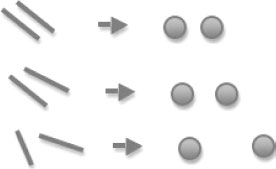
FIGURE 63.2 Correspondence between nanomagnets (MFC) and vision problem formulation. On the left are sample arrangements of pairs of straight lines and on the right are the corresponding nanomagnet placements whose interactions match the affinities between the lines. (J. Pulecio, S. Bhanja, and S. Sarkar, An experimental demonstration of the viability of energy minimizing computing using nano-magnets, Proc. 11th IEEE International Conference on Nanotechnology, Portland, OR, August 15–18, © (2011) IEEE. With permission.)
Let the matrix Λ be constructed out of given affinities such that: Λrs=(Aij)2/. We desire to find the coordinate of each point in a 2D space, which we denote by the matrix of the coordinate vector, XMDS = [x1, …, xN], such that
(63.7) |
(63.8) |
with I as the identity matrix and as the vector of ones. This operator H is referred to as the centering operator. These coordinates X can be arrived at by the classical MDS scheme [32]. The solution is based on the singular value decomposition of the centered distance matrix MDS where VMDS, ΔMDS are the eigenvectors and eigenvalues, respectively. Assuming that the centered distance matrix represents the inner product distances of a Euclidean distance matrix, the coordinates are given by
(63.9) |
Note that we have dropped the constant of proportionality, c, since the energy minimizing solutions are invariant to scaling of the original function. Our nanomagnet selection solution is given by the first two rows of XMDS; each column of this matrix gives us the coordinates of the corresponding nanomagnet to consider.
The computational overhead of this synthesis step is linear in the number of the image features. This replaces the complexity of the software solution to the minimization problem.
An Si wafer was coated with PMMA (poly/methyl methacrylate) via a Laurell Technologies WS-400A-8NPP/Lite Spin Processor. A single thin layer of 950 molecular weight PMMA in anisole was spun with a resulting thickness of approximately 120 nm. Afterward, it was baked in an oven which provided even heat over the entire wafer to evaporate any residual solvent. The magnetic field-based computing (MFC) systems were designed using DesignCAD2000 NT. The most effective line spacing, exposure doses, points, and focus were determined by using the diagnostic wheel pattern. The sample was then loaded into a JOEL 840 m retrofitted with the NPGS lithography system and a beam blanker for pattern exposure. Subsequently, the sample was unloaded for development in MIBK:Isopropanol 1:3, after which a thin Permalloy film was deposited via a Varian Model 980-2462 electron beam evaporator. A vacuum of about 2 µTorr was achieved and evaporation was conducted at a fast rate to reduce contamination. Liftoff was accomplished by placing the sample coated with Permalloy in a heated ultrasonic acetone bath for approximately 15 min.
Figure 63.3a shows an example of a vision problem where we have to find the visually salient subset of straight lines—the three parallel lines in the middle. Figure 63.3b shows the placement of magnets that can be used to solve these problems. The magnetostatic coupling between the magnets matches the pairwise affinities of the lines. Each line is represented by a magnet. The white circles represent magnetic nano-disks, enumerated from the left to the right. The disks were made of permalloy with the thickness much less than the lateral dimensions to force in-plane single domain magnetic dipole moments. The experiment would proceed by applying an external magnetizing field along a particular direction. Afterward, the field would be removed and the magnetic cells would be allowed to settle into a ground state as shown in Figure 63.3c. The natural tendency for magnetic energy is to be minimized, in this case primarily due to magneto-static coupling. It would lead magnets 1–3, to arrange themselves in a ferromagnetic fashion. It would also be possible for magnet 4 to experience a degree of coupling with magnets 1–3 which could be demonstrated via an antiferromagnetic coupling. The coupling exhibited among magnets 1–3 is expected since the inter-spacing distance is smaller than that of magnets 4 and 5. Our experimental measurements do indeed demonstrate this to be the case.
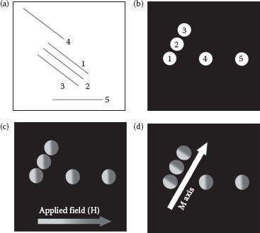
FIGURE 63.3 Read-out scheme for validation. (a) The vision problem: find the visually salient lines. (b) Equivalent magnet arrangement with a similar Hamiltonian as the vision problem. The disks correspond to the lines. (c) Magnetic initialization of the MFC system into a possible ground state of the system after the external field is removed. (d) If the magnetization is taken along axis M, the magnetization component of nanodisks 1, 2, and 3 will be larger than those of 4 and 5. (J. Pulecio, S. Bhanja, and S. Sarkar, An experimental demonstration of the viability of energy minimizing computing using nano-magnets, Proc. 11th IEEE International Conference on Nanotechnology, Portland, OR, August 15–18, © (2011) IEEE. With permission.)
If the magnetization vector of each magnet is taken along axis M, as shown in Figure 63.3d, the magnetization of magnets 1–3 would be greater than those of magnets 4 and 5. As mentioned previously, this magnetic interaction can be modeled via a quadratic term and is computationally intensive but occurs naturally in the physical world, at least on the order of nanoseconds. The magnetostatic quadratic term is inversely proportional to the quadratic edge affinity, which determines the salient features of the image. So by setting appropriate affinity thresholds, the edges corresponding to magnets 1–3 would be regarded as a significant grouping, while magnets 4 and 5 would not.
The size, spacing, and placement all correlated to the features of an image; therefore, proper fabrication of a design was imperative. We were able to achieve the accuracy of these parameters for the system shown in Figure 63.3, although on a larger scale, there were instances where some common irregularities associated with the electron beam fabrication process occurred. It is important to note how all these parameters affect the ability of a field-based system to couple and therefore extract salient features. The magnetic nanodisks used throughout the experiments were made of permalloy with negligible magnetocrystalline anisotropy. The circular shape combined with the absence of magnetocrystalline anisotropy allows for a nano-disk to have an easy axis of magnetization of 360° in-plane. For the proof of concept, the thickness was reduced to try to induce an in-plane single domain magnetic moment. The in-plane moments would couple with neighbors through magneto-static interactions. Figure 63.4a shows MFM phase graphs with corresponding images of the possible states. There is an interesting dynamic between the formation of a vortex or single domain moment in nanodisks, which is a formulation of material, diameter, neighboring elements, and thickness. Indeed, a complete implementation of magnetic field computation could benefit from the ability to switch between the single domain and vortex states, particularly because the vortex state exhibits no in-plane stray field at rest. This would essentially remove any participation of a nanodisk (in the vortex state) from the computational process. For the purpose of these experiments, the goal was to create in-plane dipole interactions through single domain magnetic moments.
Figure 63.5a and b shows AFM and MFM images of the fabricated cells scanned along three directions. To ensure a single domain magnetic dipole moment and to mitigate vortex states, engineering of the shape anisotropy should be such that the out-of-plane magnetization component of the vortex core should produce higher demagnetization energy than that of an in-plane single domain state. The average dimensions of the nanomagnetic disks were approximately 130 nm in diameter and 20 nm thick and are referred to as magnets from the left to the right. As desired, the three leftmost magnets (1, 2, 3) during all the three different scan directions were in a single domain state, with their magnetic configurations unaltered. This is due to the ferromagnetic dipole–dipole coupling between nearby neighbors that reduces the susceptibility of the nanomagnets to the stray field emanating from the magnetically coated proximal probe.
When analyzing the two right-most magnets (magnets 4 and 5), which should be in a decoupled single domain state due to the distance in between their nearest neighbors, a pinwheel magnetization is observed. This was due to the sample–probe interaction which caused the nanodisks to flip their magnetization during data acquisition, signifying a weak interaction with the neighboring elements. Even though the probe tip altered the magnetic state of the nanodisks, the single domain moment can still be extrapolated via the presence of strong dipoles. By retracing the scanning process of the tip with a scan angle of 0, as shown in Figure 63.5b by the arrow, where the slow scan progresses from the bottom to the top and the fast scan from the left to the right, the single domain moment can be followed as it flips throughout the scan. The stray field from the scanning tip was sufficiently strong to flip the magnetization of magnet 4 at least 3 times during the scan because it was decoupled from the neighboring elements. A similar process altered the magnetization of magnet 5 and the different flipping behavior is explained by a preferred magnetization axis in the vertical direction and is detailed in Figure 63.6b. This becomes evident once the scan angle is 90 and the slow scan is in the vertical direction. Magnet 5 flipped once during the scan, in a similar fashion to magnet 4, with a scan angle of 0. The development of structural minor and major axes in the elliptical magnets results in the introduction of shape anisotropy in the nanoelements. This alters the energy landscape of each element, and hence the different behavior, as the proximal probe traverses each element along their respective hard (minor) and easy (major) axes of magnetization.
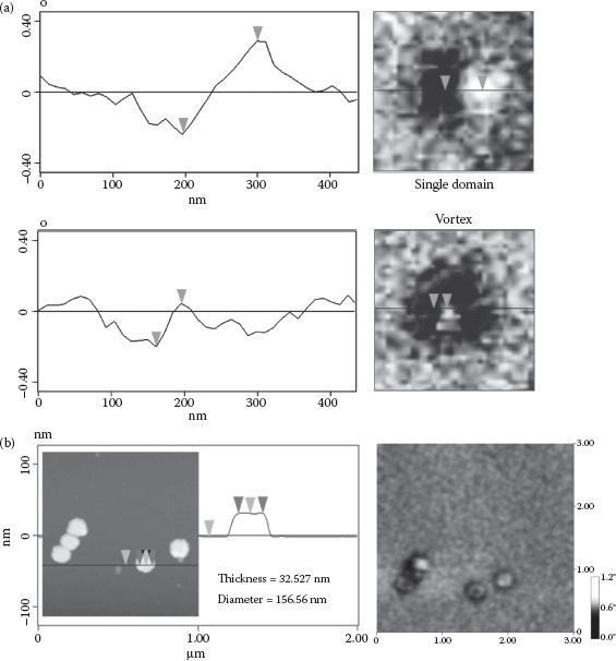
FIGURE 63.4 The phase graph and magnetic image of a single domain magnet (above) and vortex configuration (below) taken via MFM (a). The out-of-plane curl at the pole ends for the single domain state and the out-of-plane central core for the vortex state are detected by the proximal probe. Critical dimensions of the diameter and thickness are shown in (b) where both the vortex and single domain states are present.
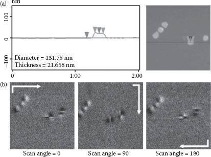
FIGURE 63.5 Fabricated nanomagnets for the vision problem. (a) AFM height amplitude image and the fabricated layout of the MFC system. As can be seen in the graph, the diameter of the measured nanodisk is 131.75 nm and the thickness is 21.658 nm. (b) Three images show MFM scans of the fabricated arrangement, scanned along different directions. (J. Pulecio, S. Bhanja, and S. Sarkar, An experimental demonstration of the viability of energy minimizing computing using nano-magnets, Proc. 11th IEEE International Conference on Nanotechnology, Portland, OR, August 15–18, © (2011) IEEE. With permission.)
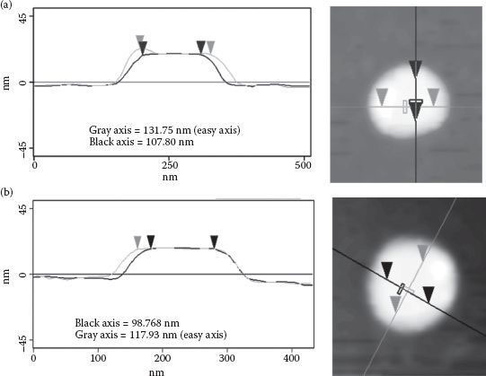
FIGURE 63.6 AFM images of major and minor axes of magnet 4 (a) and magnet 5 (b) are depicted. The major axes of the magnets create an easy axis of magnetization. This is significant when interpreting sample–tip interactions.
Magnetic field-based computing (MFC) has the potential to offer a unique solution for the quadratic minimization problem. This is unlike other implementations of magnetic logic in that it does not force the magnetostatic coupled elements to perform Boolean operations; instead, the natural tendencies of magnets to reach the lowest possible ground state for the entire system are exploited. The time necessary for the magnetic field-based systems to settle into an energy minimum is related to the relaxation time of the constituting magnetic elements (in this case on the order of nanoseconds). Excitingly, the computational time should not scale with the size/complexity of the image to process since the magnetic interactions between nanoelements are massively parallel, meaning that the relative computation time for a small system such as Figure 63.5 should be similar to a larger system such as Figure 63.7. MFC should also provide the associated benefits of other nanomagnetic logic such as radiation hardness, scalability, and low-power operation.
Here, we presented an image processing application of a quadratic problem where the grouping of low-level segments into relevant features was demonstrated. A proof-of-concept device, which consisted of five edge segments from an image, was mapped to nanomagnetic disks through a placement algorithm. The nanomagnets were fabricated and strictly adhered to placement and dimensions that correlated magnetostatic interactions to the edge affinity energies of an image. The significance of creating a nanodisk to specific dimensions was displayed by the undesired formation of preferred axes of magnetization and the formation of magnetic vortices. The strong magnetostatic interaction revealed by nanodisks 1–3 was established via the ferromagnetic coupling exhibited by the nano-magnets. Nanodisks 4–5 were strongly influenced by the MFM tip and caused the magnet moments of the magnets to flip during data acquisition. The switching of nanodisks 4–5, and the lack of variation in magnetic dipole moments of nanodisks 1–3 due to the magneto-static coupling, was determined to be a satisfactory way of qualitatively determining strong field interactions of neighboring magnets. The strong coupling exhibited between nanomagnets 1–3, which are directly mapped to the specific edges of an image, was determined to be a salient feature for segment grouping. Larger systems, such as those described in Figure 63.7, have also been fabricated and are currently being evaluated to investigate the effectiveness of MFC for perceptual organization in computer vision.

FIGURE 63.7 A more intricate system of nanomagnets for the vision problem. (a) AFM height amplitude image and the fabricated layout of the MFC system. As can be seen in the graph, the diameter of the measured nanodisk is 155.39 nm and the thickness is 9.0 nm. (b) A corresponding MFM image of the system. Note the complicated magnet structure throughout the entire system. Both the single domain and vortex states are present.
This work was supported in part by the National Science Foundation under Grant CCF 0829838.
1. National Nanotechnology Initiative. Standards for Nanotechnology. http://www.nano.gov/you/standards. Accessed: 17/05/2012.
2. International Organization for Standardization. TC 229 Nanotechnologies. http://www.iso.org/iso/iso_technical_committee?commid=381983, 2005. Accessed: 17/05/2012.
3. Intel’s 45 nm CMOS technology. Intel Technology Journal, 12(45), 2008.
4. K. J. Kuhn. CMOS scaling for the 22 nm node and beyond: Device physics and technology. In Proceedings of 2011 International Symposium on VLSI Technology, Systems and Applications, pp. 1–2. IEEE, April 2011.
5. International Technology Roadmap for Semiconductors. Executive Summary. http://www.itrs.net/Links/2011ITRS/Home2011.htm, 2011. Accessed: 18/05/2012.
6. G. Csaba, A. Imre, G. Bernstein, W. Porod, and V. Metlushko, Nanocomputing by field-coupled nano-magnets, IEEE Transactions on Nanotechnology, 1(4), 209–213, Dec. 2002.
7. A. Imre, G. Csaba, L. Ji, A. Orlov, G. Bernstein, and W. Porod, Majority logic gate for magnetic quantum-dot cellular automata, Science, 311(5758), 205–208, Jan. 2006.
8. C. Lent and P. Tougaw, A device architecture for computing with quantum dots, in Proceedings of the IEEE, 85(4), 541–557, April 1997.
9. J. C. Lusth, C. B. Hanna, and J. C. Diaz-Velez, Eliminating non-logical states from linear quantum-dot cellular automata, Mircoelectronics Journal, 32, 81–84, 2001.
10. R. Kummamuru, J. Timler, G. Toth, C. Lent, R. Ramasubramaniam, A. Orlov, G. Bernstein, and G. Snider, Power gain in a quantum-dot cellular automata latch, Applied Physics Letters, 81, 1332–1334, August 2002.
11. P. D. Tougaw and C. S. Lent, Dynamic behavior of quantum cellular automata, Journal of Applied Physics, 80, 4722–4736, Oct. 1996.
12. R. Cowburn and M. Welland, Room temperature magnetic quantum cellular automata, Science, 287(5457), 1466–1468, 2000.
13. S. Bandyopadhyay, Power dissipation in spintronic devices: A general perspective, Journal of Nanoscience & Nanotechnologies, 7(1), 168–80, 2007.
14. J. Pulecio and S. Bhanja, Magnetic cellular automata coplanar cross wire systems, Journal of Applied Physics, 107(3), 034308–034308-5, Feb. 2010.
15. M. T. Alam, S. Kurtz, M. T. Niemier, S. X. Hu, G. H. Bernstein, and W. Porod, Magnetic logic based on coupled nanomagnets: Clocking structures and power analysis, in. 8th IEEE Conference on Nanotechnology, 2008. NANO ’08, Arlington, TX, pp. 637–637, 2008.
16. D. Allwood, G. Xiong, C. Faulkner, D. Atkinson, D. Petit, and R. Cowburn, Magnetic domain-wall logic, Science, 309(5741), 1688–1692, 2005.
17. A. Csurgay, W. Porod, and C. Lent, Signal processing with near-neighbor-coupled time-varying quantum-dot arrays, IEEE Transactions on Circuits and Systems, 47, 1212–1223, Aug. 2000.
18. A. Fijany, N. Toomarian, and M. Spotnitz, Implementing permutation matrices by use of quantum dots, Tech. Rep., Jet Propulsion Laboratory, California, Oct. 2001.
19. A. Fijany, N. Toomarian, K. Modarress, and M. Spotnitz, Compact interconnection networks based on quantum dots, Tech. Rep., Jet Propulsion Laboratory, California, Jan. 2003.
20. A. Fijany, N. Toomarian, K. Modarress, and M. Spotnitz, Hybrid vlsi/qca architecture for computing FFTs, Tech. Rep., Jet Propulsion Laboratory, California, Apr. 2003.
21. T. Cole and J. C. Lusth, Quantum-dot cellular automata, Progress in Quantum Electronics, 25, 165–189, 2001.
22. W. H. Lee and P. Mazumder, Color image processing with quantum dot structure on a multi-peak resonant tunneling diode, in 7th IEEE Conference on, Nanotechnology, 2007. IEEE-NANO 2007. pp. 1161–1165, Aug. 2007.
23. K. Karahaliloglu, S. Balkir, S. Pramanik, and S. Bandyopadhyay, A quantum dot image processor, IEEE Transactions on Electron Devices, 50, 1610–1616, 2003.
24. S. Sarkar and S. Bhanja, Direct quadratic minimization using magnetic field-based computing, in 2008 IEEE International Workshop on, Design and Test of Nano Devices, Circuits and Systems, Cambridge, MA, pp. 31–34, Sept. 2008.
25. A. Moini, Vision Chips. Springer, Netherlands, 2000.
26. J. Kim, M. Kim, S. Lee, J. Oh, S. Oh, and H. Yoo, Real-time object recognition with neuro-fuzzy controlled workload-aware task pipelining, Micro, IEEE, 29(6), 28–43, 2009.
27. W. Grimson, Object Recognition by Computer: The Role of Geometric Constraints. MIT Press, Cambridge, MA, 1991.
28. D. Clemens and D. Jacobs, Model group indexing for recognition, in 1991. Proceedings CVPR’91. IEEE Computer Society Conference on, Computer Vision and Pattern Recognition, Maui, HI, pp. 4–9, IEEE, 1991.
29. A. Bennett and J. Xu, Simulating collective magnetic dynamics in nanodisk arrays, Applied Physics Letters, 82, 2503, 2003.
30. M. Levitt, Spin Dynamics: Basics of Nuclear Magnetic Resonance. Wiley, Chichester, UK, 2001.
31. J. Pulecio, S. Bhanja, and S. Sarkar, An experimental demonstration of the viability of energy minimizing computing using nano-magnets, Proc. 11th IEEE International Conference on Nanotechnology, Portland, OR, August 15–18, 2011.
32. M. Cox and T. Cox, Multidimensional scaling, in Handbook of Data Visualization, C.-H. Chen, W. Hardie, and A. Unwin, (eds.) Springer-Verlag, Berlin, Heidelberg, pp. 315–347, 2008.
33. P. Indyk and J. Matousek, Low-distortion embedding of finite metric space, Handbook of Discrete and Computational Geometry, p. 177, 2004.
34. J. Nievergelt and N. Deo, Metric graphs elastically embeddable in the plane, Information Processing Letters, 55(6), 309–315, 1995.
35. J. Bourgain, On Lipschitz embedding of finite metric spaces in Hilbert space, Israel Journal of Mathematics, 52(1), 46–52, 1985.