
CONTENTS
65.3.1 Effect of Impurity Scattering
65.3.2 Effect of Dangling Bond Scattering
For more than a decade, there have been many experiments reporting anomalies that appear at noninteger values of the quantized conductance G0 in the ballistic conductance regime of quantum point contacts (QPCs) based on GaAs. These include the observation of an anomalous plateau at G ≅ 0.5 G0 [1, 2, 3 and 4] and the well-known “0.7 structure” [5]. The majority of the theoretical models link them to spontaneous spin polarization in the QPC [6, 7 and 8]. Recently, we used a nonequilibrium Green’s function (NEGF) approach to study in detail the ballistic conductance of asymmetrically biased, side-gated QPCs in the presence of lateral spin–orbit coupling (LSOC) and strong electron–electron interactions. We performed simulations for a wide range of QPC dimensions and gate bias voltages [9].
Various conductance anomalies appeared below the first quantized conductance plateau (G0 = 2e2/h); these occur due to spontaneous spin polarization in the narrowest portion of the QPC. We have found that the number of conductance anomalies increases with the aspect ratio (length/width) of the QPC constriction. These anomalies are fingerprints of spin textures in the narrow portion of the QPC [9].
Since the early 1990s, there has been a considerable amount of work studying the influence of impurity scattering on the quantized conductance plateaus of QPCs [10, 11, 12, 13, 14, 15 and 16]. We recently showed that asymmetric LSOC, resulting from the lateral in-plane electric field of the confining potential of a side-gated QPC, can be used to create a strongly spin-polarized current by purely electrical means [17] in the absence of an applied magnetic field. Using an NEGF analysis of a small model QPC [18], three ingredients were found to be essential for generating a strong spin polarization: an asymmetric lateral confinement, an LSOC induced by the lateral confining potential of the QPC, and a strong electron–electron (e–e) interaction.
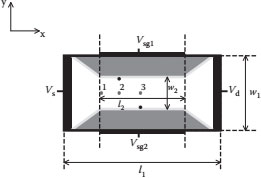
FIGURE 65.1 Schematic of the QPC configuration used in the numerical simulations. The width and length of the narrow portion of the QPC are equal to w2 and l2, respectively. In the simulations, we used w2, l2, w1, and l1 = 16, 32, 48, and 64 nm, respectively. The circles in the middle of the narrow portion of the QPC represent impurities with coordinates y1 = w1/2 and x1 = 16, 24, and 32 nm, respectively. The two circles on the side walls are dangling bonds located one-fourth (top side wall) and one-half of the way (bottom side wall) from the left entrance to the narrow portion of the QPC.
In this chapter, we investigate the influence of impurities and dangling bonds on the conductance anomalies in GaAs QPCs created by side gates, in the presence of LSOC. We consider the effects of attractive and repulsive scatterers in the narrow portion of the QPC and dangling bonds on its side walls, as depicted in Figure 65.1.
One of the main ingredients needed to generate spin polarization in the central portion of a QPC is an asymmetric potential profile in the channel. It is expected that off-center impurities can lead to such an asymmetry even for a symmetric bias voltage on the two side gates. In this case, our simulations predict that conductance anomalies can be observed in an otherwise perfectly symmetric QPC due to unwanted impurities in the channel.
The conductance through a QPC was calculated using an NEGF approach, described in detail earlier [2,9,19]. At the interface between the rectangular region of size w2 × l2 and a vacuum, the conduction band discontinuities at the bottom and the top interface were modeled using a smooth conduction band change over a small distance d from ΔEc(y) at the trench/channel interface down to zero in the channel. This gradual change in ΔEc(y) is responsible for the LSOC that triggers the spin polarization of the QPC in the presence of an asymmetry in Vsg1 and Vsg2. We modeled ΔEc(y) for the bottom side wall in Figure 65.1 as
(65.1) |
and, for the top side wall, we used
(65.2) |
where d represents the distance (in nm) over which the conduction band profile varies from its value inside the quantum wire to that of the vacuum region. In our simulations, we used d = 1.6 nm. A similar grading was also used along the walls going from the wider part of the channel to the central constriction of the QPC (Figure 65.1).
In our simulations, we model the e–e interaction Vint (r,r′) using the following nonlocal 2D screened potential [20]:
(65.3) |
where λ is the screening length, H0(x) is the Struve function, and N0(x) is a Bessel function of the second kind. The LSOC parameter β (see appendix) and screening length λ were set equal to 5 Å2 and 5 nm, respectively.
For an impurity or dangling bond located at location (x1, y1), we model the potential energy in the two dimensional electron gas (2DEG) as
(65.4) |
where Δ = q/4 πε0 εrU0 and U0 is the maximum strength of the impurity potential.
For an attractive impurity, we use the above expression with a negative sign. We use εr = 12.9, the relative dielectric constant of GaAs. In all simulations, the source potential Vs = 0 V, and the potential at the drain contact Vd = 0.1 mV. An asymmetry in the QPC potential confinement is introduced by taking Vsg1 = 0.2 V + Vsweep and Vsg2 = −0.2 V + Vsweep and the conductance of the constriction was studied as a function of the sweeping (or common mode) potential, Vsweep. The conductance of the QPC was then calculated using the NEGF with a nonuniform grid configuration that contained more grid points at the interface of the QPC with a vacuum. All calculations were performed at a temperature T = 4.2 K. The screening length λ in Equation 65.1 was set to 5 nm and assumed to be independent of the gate potentials. Hereafter, we also calculate the spin conductance polarization α = [G↑–G↓]/[G↑ + G↓], where G↑ and G↓ are the conductances due to the majority and minority spin bands, respectively. We study how the maximum of alpha is affected by the strength, polarity, and locations of the impurities and dangling bonds.
65.3.1 EFFECT OF IMPURITY SCATTERING
Figure 65.2 is a plot of the conductance as a function of Vsweep for a QPC containing an impurity at location 3 in Figure 65.1. Shown for comparison is the conductance with no impurity in the channel. The conductance anomalies are highly sensitive to the strength and type of impurity (attractive and repulsive). All the curves show a conductance anomaly around 0.5 G0 followed by a negative differential resistance region (NDR) and a second anomaly somewhere between 0.5 and 1 G0. The peak-to-valley ratio of the NDR after the 0.5 G0 increases with the strength of the impurity potential for the attractive impurity potential. The opposite trend is observed for a repulsive impurity. Figure 65.2 shows that there is a substantial shift of the conductance along the common signal Vsweep for an impurity that is either attractive or repulsive.
In QPC experiments, the charge state of an impurity is often affected by sample handling, such as temperature cycling, when the sample is brought back to room temperature between low temperature measurements. This typically leads to markedly different conductance traces for identical bias conditions, and recently, we observed this phenomenon while studying the conductance of InAs-based QPCs in the presence of LSOC, while varying the asymmetric bias applied between the two side gates [21]. Thermal cycling is expected to change the charge state of either the remote impurities used in the modulation doping to form the 2DEG or in the charge state of dangling bonds formed on the side walls of the QPC during etching, or even due to a single impurity located directly in the path of the current flow. The sensitivity of the conductance anomalies to the impurity location (points 1, 2, and 3 in Figure 65.1) in the central portion of the QPC is illustrated in Figure 65.3.
FIGURE 65.2 Conductance as a function of Vsweep for a QPC containing an impurity (either attractive or repulsive) at location 3 in Figure 65.1. The three leftmost curves correspond to an attractive impurity with scattering strength (U0) equal to (from left to right) −30, −20, and −10 meV, respectively. The three rightmost curves correspond to a repulsive impurity with scattering strength (U0) equal to (from left to right) 10, 20, and 30 meV, respectively. The middle curve corresponds to the case of no impurity in the channel.
The maximum value of α was found to be located near the first maximum in the conductance plots in Figures 65.2 and 65.3. In Figure 65.1, αmax changes by 6% (from 0.989 to 0.927) when U0 varies from −30 to 30 meV. The change in αmax is only 4% (from 0.976 to 0.948) when U0 changes from −20 to 20 meV, and less than 1% (from 0.976 to 0.97) when U0 changes from −10 to 10 meV. This dependence of αmax on the type and strength of an impurity, even though by just a few percent, could lead to a substantial reduction in the ON/OFF conductance ratio of a spin valve built of two QPCs in series. Interestingly, the value of αmax is larger (smaller) in the presence of an attractive (repulsive) impurity compared to the case of no impurity in the channel, for which αmax = 0.973. To reach a larger value of αmax, a tunable repulsive impurity potential could be generated through the use of a negatively biased scanning tunneling microscope (STM) tip on top of the narrow portion of the QPC.
FIGURE 65.3 Conductance as a function of Vsweep for a QPC containing an impurity in the central portion of the channel at locations 1, 2, and 3 in Figure 65.1. The strength of the scattering potential is −30 meV for the three leftmost curves (attractive impurity) and 30 meV for the three rightmost curves (repulsive impurity). The full, dashed, and dot-dashed curves correspond to an impurity at locations 1, 2, and 3, respectively, in Figure 65.1.
FIGURE 65.4 Conductance as a function of Vsweep for a QPC containing two off-center repulsive impurities located at (x1, y1) = (16 nm, 28 nm) and (x2, y2) = (32 nm, 28 nm). We used Vsg1 = −0.2 V + Vsweep and Vsg2 = 0.2 V + Vsweep.
In Figure 65.4, we plot the conductance versus Vsweep for a QPC containing two repulsive impurities located at (x1, y1) = (16 nm, 28 nm) and (x2, y2) = (32 nm, 28 nm), that is, slightly off-center. In this case, a reverse polarity was used, that is, Vsg1 = −0.2 V + Vsweep and Vsg2 = 0.2 V + Vsweep, the overall potential energy in the narrow portion of the QPC is larger closer to gate 1 and near the conductance anomaly, the spin-down electrons are the majority carriers. We found αmax = −0.956, still a rather large value despite the two impurities in the channel.
Figure 65.5 illustrates that even for the case of asymmetric bias on the two gates (Vsg1 = Vsg2 = 0.0 V + Vsweep), a conductance anomaly is found with the same two off-center repulsive impurities as in the previous figure. In this case, the potential energy maximum is also closer to gate 1 in the narrow portion of the QPC and the spin-down electrons are the carriers in the channel near the conductance anomaly. This simulation shows that even a slight asymmetry due to unwanted impurities can lead to spin polarization in an otherwise perfectly symmetric channel.
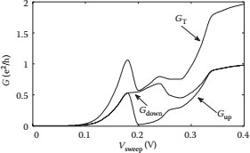
FIGURE 65.5 Conductance as a function of Vsweep for a QPC containing two repulsive impurities impurities located at (x1, y1) = (16 nm, 28 nm) and (x2, y2) = (32 nm, 28 nm) for the case of a symmetrical bias condition, that is, Vsg1 = Vsg2 = 0.0 V + Vsweep.
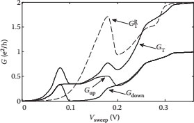
FIGURE 65.6 Conductance as a function of Vsweep for a QPC containing two dangling bonds shown as dark dots in Figure 65.1. The strength of the dangling bond potential U0 was set to 200 meV. The contributions from the up-spin and down-spin electrons to the total conductance GT are shown for the case Vsg1 = −0.2 V + Vsweep and Vsg2 = 0.2 V + Vsweep. The dashed curve is the conductance , that is, for the case Vsg1 = 0.2 V + Vsweep and Vsg2 = −0.2 V + Vsweep.
65.3.2 EFFECT OF DANGLING BOND SCATTERING
In Figure 65.1, the black circles represent the two dangling bonds considered in our simulations. The first dangling bond has coordinates , that is, it is located one-fourth of the way from the left side in the narrow portion of the QPC and in the middle of the top side wall interface modeled with Equation 65.1. The second dangling bond has coordinates (x2, y2) = ((l1 − l2)/2) ((w1 − w2)/2) (d/2), (that is, it is located in the middle of the narrow portion of the QPC on the bottom side wall interface modeled with Equation 65.2.
Figure 65.6 shows a plot of the total conductance GT = G↑ + G↓ versus Vsweep for the case of two dangling bonds. The strength of a dangling bond potential U0 was set equal to 200 meV. The full curve for Gtot corresponds to the case where Vsg1 = −0.2 V + Vsweep and Vsg2 = 0.2 V + Vsweep. Also shown in Figure 65.6 are the contributions from G↑ and G↓, which differ substantially for Vsweep in the range from 0.02 to 0.1 V. Figure 65.6 shows conductance anomalies around 0.3 G0 and 0.36 G0 and also a shoulder in the plot around 0.75 G0. The dashed curve in Figure 65.6 is a plot of r reverse asymmetry, that is, with Vsg1 = 0.2 V + Vsweep and Vsg2 = −0.2 V + Vsweep. The difference between the two curves for GT is due to the asymmetry in the potential energy profile in the narrow portion of the QPC prior to the application of the different biases on the side gates.
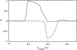
FIGURE 65.7 Spin polarization of the conductance α as a function of Vsweep calculated using the results in Figure 65.6. The full and dashed curves are α for the case of Vsg1 = −0.2 V + Vsweep and Vsg2 = 0.2 V + Vsweep and Vsg1 = 0.2 V + Vsweep and Vsg2 = −0.2 V + Vsweep, respectively.
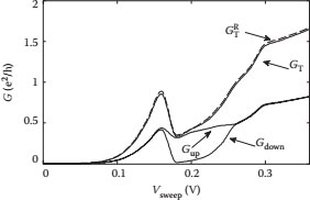
FIGURE 65.8 Same as Figure 65.6 for the same dangling bonds but with an impurity potential U0 = 100 meV.
The spin conductance polarization α for the two biasing cases Vsg1 = ±0.2 V + Vsweep and Vsg2 = ±0.2 V + Vsweep is shown in Figure 65.7. When Vsg1 = −0.2 V + Vsweep and Vsg2 = 0.2 V + Vsweep, α reaches a maximum of 0.97 for Vsweep = 0.1 V. For this value of Vsweep, GT = 0.47 G0. When Vsg1 = 0.2 V + Vsweep and Vsg2 = −0.2 V + Vsweep, α is negative because the role of the majority and minority spin bands are flipped compared to the previous case and α reaches a minimum of −0.85 for Vsweep = 0.2 V. For this value of Vsweep, . The conductance curve versus Vsweep is different for the two polarities of the bias asymmetry between the gates. Despite the presence of the dangling bonds, α is quite large, indicating a substantial amount of spin polarization in the QPC channel.
The simulations were repeated for a lower value of the dangling bond impurity strength U0 = 100 meV. The plots of the conductance and spin polarization α versus Vsweep are shown in Figures 65.8 and 65.9, respectively. In this case, there is hardly any difference between the two conductance curves for the two biasing configurations, cases Vsg1 = ±0.2 V + Vsweep and Vsg2 = ±2 V + Vsweep. The plot of α versus Vsweep for the two biasing configurations is the reverse of one another, indicating that spins of opposite polarities are the major carriers when the biasing conditions are flipped; α reaches a maximum of 0.89 for Vsweep = 0.18 V at which GT = 0.17 G0. For the opposite polarity, α reaches an absolute minimum of −0.90 for Vsweep = 0.18 V at which . These simulations show that a hysteresis in the conductance curve, when flipping the polarity of the bias asymmetry ΔVG = VG1–VG2, can only be observed if the dangling bond scattering potential is sufficiently large.
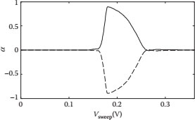
FIGURE 65.9 Same as Figure 65.7 for the same dangling bonds but with an impurity potential U0 = 100 meV.
In this chapter, the NEGF formalism was used to study how the spin polarization is affected by the presence of impurities in the central portion of the QPC and by dangling bonds on the side walls. It is found that the number, location, and shape of the conductance anomalies occurring below the first quantized conductance plateau (G0 = 2e2/h) are strongly dependent on the nature (attractive or repulsive) and locations of the impurities and dangling bonds. Our simulations show that a spin conductance polarization over 90% can be achieved despite the presence of impurities and dangling bonds and that this maximum is not necessarily reached where the conductance of the channel is equal to 0.5 G0. For QPCs with impurities off-center, a conductance anomaly appears below the first integer step even for the case of symmetric bias on the two side gates. These results are of practical importance if QPCs in series are to be used to fabricate all-electrical spin valves with a large ON/OFF conductance ratio.
1. W.K. Hew et al., Spin incoherent transport in quantum wires, Phys. Rev. Lett. 101, 036801, 2008.
2. R. Crook et al., Conductance quantization at a half-integer plateau in a symmetric GaAs quantum wire, Science 312, 1359, 2006.
3. D.J. Reilly et al., Density-dependent spin polarization in ultra-low-disorder quantum wires, Phys. Rev. Lett. 89, 246801, 2002.
4. S. Kim, Y. Hashimoto, Y. Iye, and S. Katsumoto, Evidence of spin-filtering in quantum constrictions with spin-orbit interaction, arXiv: 1102.4648v1, 2011.
5. A.P. Micolich, What lurks below the last plateau: Experimental studies of the 0.7 × 2e2/h conductance anomaly in one-dimensional systems, J. Phys. Cond. Matter 23, 443201, 2011.
6. P. Jaksch, I. Yakimenko, and K.-F. Berggren, From quantum point contacts to quantum wires: Densityfunctional calculations with exchange and correlation effects, Phys. Rev. B 74, 235320, 2006.
7. K.J. Thomas et al., Possible spin polarization in a one-dimensional electron gas, Phys. Rev. Lett. 77, 135, 1996.
8. D.J. Reilly, Phenomenological model for the 0.7 conductance feature in quantum wires, Phys. Rev. B 72, 033309, 2005.
9. J. Wan, M. Cahay, P. Debray, and R.S. Newrock, Spin texture in quantum point contacts in the presence of lateral spin orbit scattering, J. Nanoelectron. Optoelectron. 6, 95, 2011.
10. J. Faist, P. Gueret, and H. Rothinzen, Observation of impurity effects on conductance quantization, Superlattices Microstructures 7, 349, 1990.
11. C.S. Chu and R.S. Sorbello, Effect of impurities on the quantized conductance of narrow channels, Phys. Rev. B 40, 5941, 1989.
12. E. Tekman and S. Ciraci, Ballistic transport through a quantum point contact: Elastic scattering by impurities, Phys. Rev. B 42, 9098, 1990.
13. J.A. Nixon, J.H. Davies, and H.U. Baranger, Breakdown of quantized conductance in point contacts calculated using realistic potentials, Phys. Rev. B 43, 12638, 1991.
14. A. Grincwajg, G. Edwards, and D.K. Ferry, Quasi-ballistic scattering in quantum point contact systems, J. Phys. Condens. Matter 9, 673, 1997.
15. M.J. Laughton, J.R. Barker, J.A. Nixon, and J.H. Davies, Modal analysis of transport through quantum point contacts using realistic potentials, Phys. Rev. B 44, 1150, 1991.
16. J.C. Chen, Y. Lin, K.T. Lin, T. Ueda, and S. Komiyama, Effects of impurity scattering on the quantized conductance of a quasi one-dimensional quantum wire, Appl. Phys. Lett. 94, 012105, 2009.
17. P. Debray et al., All-electric quantum point contact spin-polarizer, Nat. Nanotechnol., 4, 759–764, 2009.
18. J. Wan, M. Cahay, P. Debray, and R.S. Newrock, On the physical origin of the 0.5 plateau in the conductance of quantum point contacts, Phys. Rev. B 80, 155440, 2009.
19. S. Datta, Electron Transport in Mesoscopic Systems, Cambridge University Press, New York, 1995.
20. G. Giuliani and G. Vignale, Quantum Theory of the Electron Liquid, Cambridge University Press, Cambridge, 2005.
21. P.P. Das, N. Bhandari, J. Wan, J. Charles, M. Cahay, K.B. Chetry, R.S. Newrock, and S.T. Herbert, Influence of surface scattering on the anomalous plateaus in an asymmetrically biased InAs/InAlAs quantum point contact, Nanotechnology 23, 215201, 2011.
22. J. Wan, M. Cahay, P. P. Das, and R. S. Newrock, Influence of impurity scattering on the conductance anomalies of quantum point contacts with lateral spin-orbit coupling, Proc. 11th IEEE International Conference on Nanotechnology, August 15–18, Portland, Oregon, pp. 1395–1398, 2011.