
CONTENTS
68.2 Electrical Currents on the Nanoscale
68.3 Atomic-Scale Device Structures
68.4 Quantum-Mechanical Device Modeling
68.4.2 Electronic Structure Methods for Atomic-Scale Device Modeling
68.4.3 Electrostatics and Boundary Conditions
Even though the active components of semiconductor devices have been shrunk down radically over the past decade, to the point where certain feature sizes are in the range of 30–40 nm, the motion and behavior of electrons are still reasonably well described by semiclassical models—Ohm’s law coupled with macroscopic electrostatic models, drift–diffusion equations, and so on. The number of carriers is still large enough that quantum fluctuations are averaged out statistically, and the materials involved can, for the most part, be characterized by bulk material parameters. In this domain, technology computer aided design (TCAD) models are an essential tool to model and predict the physical properties of device components.
However, as the downscaling of the gate length, oxide thickness, and other crucial device parameters continues, quantum effects that are not captured by the semiclassical models start to play a dominating role. Furthermore, the device functionality of, for example, tunnel field-effect transistors (TFET) is a consequence not just of the properties of a single material but rather of the interfaces formed between different semiconductors and/or metals. The smaller the active regions are made, the larger the effects of individual atomic defects, vacancies, dislocations, and grain boundaries also become, and these can significantly change the properties of the Schottky barrier height of an interface, or the ability of a thin dielectric layer to block the leakage current. This can have devastating consequences for the device variability during the fabrication process, and for reliability under operating conditions. Adding to this the veritable zoo of “exotic” elements (including structures like graphene) that are currently part of the palette of options for device engineers, it becomes increasingly clear that new models need to be incorporated into the design workflow used for developing novel transistors, memory elements, radiofrequency resonators, and so on.
From a physical perspective, there are two fundamental factors to consider. First of all, atomic-scale defects are discrete in nature, as opposed to the continuum material description used in TCAD models. Moreover, the properties of an interface between two or more materials, or, for instance, a thin dielectric layer embedded between two other materials, cannot simply be deduced from the combined properties of the different materials. In fact, the most advanced gate stacks today contain just a few atomic layers of high-κ dielectric materials like HfO2, and it is highly questionable whether these layers can be described reliably by the same parameters that apply to bulk HfO2. In the case of nanowires, the influences of surface adsorbants, interface roughness, or diameter variation (Figure 68.1) are also effects that require a detailed investigation on the atomic scale.
Second, as the length scales approach the mean-free path of the material, electrons will not travel diffusively across the barrier anymore. Instead, the charge transport through the barrier becomes a tunneling process, and the electrons no longer behave as particles, but must be described as wave functions. In the ultimate limit, where scattering can be neglected, we thus have a ballistic, coherent tunneling process, and the corresponding transmission probability and current can only be computed quantum-mechanically; Ohm’s law is no longer valid, and we cannot define uniquely the conductivity of the material, as it becomes bias-dependent with a nonlinear current–voltage relation. The tunneling current is furthermore strongly influenced by the presence of atomic-scale defects, which act as elastic scattering centers. Inelastic scattering may, of course, also be present in the quantum-mechanical picture, especially when the mean-free path is comparable to the tunneling barrier thickness.
To capture both sets of effects, it is necessary to consider the system as a whole, with all the different materials interacting and influencing each other in a way that can only be described with quantum-mechanical atomistic models.
In addition, with the introduction of new materials such as low-κ dielectrics with low thermal conductivity, the need arises for combined thermal, mechanical, optical, and electrical modeling, as stressed in the International Technology Roadmap for Semiconductors (ITRS) [1], since these properties are no longer necessarily independent of each other, especially as more and more functionality becomes integrated on a single chip. The mechanical and thermal properties can to a large extent still be treated classically, but atomistically—or rather, the large computational cost for quantum-mechanical models leaves us no other solution for the moment. An important stumbling block here, however, is the fact that very few reliable potentials exist for most of the materials of interest, and new material combinations are introduced all the time. A methodology that allows for the derivation of new potentials for novel materials is therefore necessary to facilitate this effort, and in this process, first-principles modeling will play an important role for the fitting of the potentials.
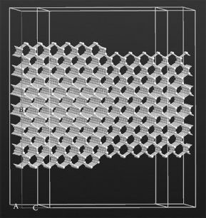
FIGURE 68.1 Model for a step-like change in diameter in a Si (110) nanowire.
It thus appears evident that there is a strong need for a new generation of device simulation tools, which can incorporate methodologies that are capable of integrating different methods, deal with combinations of metals, semiconductors, as well as organic materials, and that can compute both electronic and thermal transport properties, as well as mechanical and optical properties, in realistic nanoscale device geometries, taking atomistic features into account. Such tools will be an essential enabling technology for the nodes ahead in the ITRS, which mentions “atomistic” or “atomic-scale” modeling at least 15 times in the latest section on Modeling & Simulation [1]. This applies not only to the far-out nodes at 10 or 5 nm but also the more imminent ones.
We will review here some aspects of the state-of-the-art modeling of currents from a quantum-mechanical atomistic perspective. Particular focus will be placed on recent developments of relevance for more traditional (yet nanoscale) semiconductor materials and device types, although the principles apply very well also to more exotic device designs based on molecular junctions, nanotubes, graphene, and so on.
68.2 ELECTRICAL CURRENTS ON THE NANOSCALE
It is interesting to note that the two effects discussed above, that is, the discrete nature of sources of scattering and the atomistic effects involved in the combination of different materials to form an interface on the one hand, and the wave nature of electrons on the other, can individually be treated with simpler models. Using effective mass theory, either in a simple single-band description or with more sophisticated models like kp, the quantum-mechanical electronic structure of quantum wells and other heterojunctions can be computed while still assuming that the materials are homogeneous, and thus can be described with a set of material parameters, typically derived from bulk properties. Conversely, classical molecular mechanics simulations are used extensively to model growth processes and other properties of collections of atoms (usually very many)—provided that relevant potentials are available. Complications arise, however, when we combine the quantum effects with the atomistic features, and a more complete description will be needed.
In the classical picture of electrical conductivity, electrons are accelerated by an electric field caused by the voltage bias applied across the material, but owing to a series of scattering events—occurring with a frequency determined by the mean-free path of the material, which is typically of the order of 50–100 nm—the conductivity remains finite. At the nanoscale—that is, in the limit where the feature sizes are significantly smaller than the mean-free path of the material—a completely different picture emerges. The electronic current must now be viewed as the propagation of a quantum-mechanical wave function. Concepts like resistivity or conductivity no longer have any meaning since they arise via scattering processes that now do not have time to occur as the electron traverses the device. Instead, we must speak of conductance as a measure of the “quality” by which the material (or, rather, the device as a whole) can conduct electricity. Conductance is a central concept in the Landauer–Büttiker formalism [2], which is the standard approach for describing coherent ballistic or tunneling currents in a complex structure containing several leads. In this picture, the current in a two-terminal device is obtained by integrating the transmission probability T(E) (the summed transmission probability of all available channels or modes) over all energies E, weighted with the difference in the Fermi distributions of both the leads. Ignoring the details for the present discussion, in the zero-temperature limit, the expression for the current reduces to
(68.1) |
and from this expression one can derive the zero-bias conductance from the transmission at the Fermi level Ef as G = G0T(Ef), where G0 = 2e2/h = 77.48 µΩ−1 is the quantum conductance unit.
The difficulty in this formalism lies in actually computing the transmission probabilities for a real atomic-scale system, taking into account the relevant boundary conditions and self-consistent electrostatic response, with an accurate account of the electronic energy levels. This will be the topic of the following sections.
As a side comment, we note that the transmission probabilities are typically not greatly affected by the electron temperatures of the leads. One can therefore often obtain an accurate estimate of the temperature dependence of the thermionic emission current without having to recompute the transmission spectrum for each temperature. It is, however, almost always necessary to compute T(E) for each bias, that is, the linear-response assumption that T(E) is independent of the bias rarely holds, even for small values of the bias.
68.3 ATOMIC-SCALE DEVICE STRUCTURES
Modeling of nanoscale structures such as nanowires, nanotubes, graphene devices, molecular junctions, and ultrathin dielectric junctions has evolved over the last decade into a position where several thousand atoms can now be simulated with atomistic, quantum-mechanical methods, using methods ranging from density-functional theory (DFT) to tight-binding models.
With the introduction of nonequilibrium techniques, it has furthermore become possible to compute not only the electronic structure properties of various materials, but also the transport properties of device-like structures under an applied finite bias [3, 4 and 5]. In these models, the system geometry is generally made up of two conducting electrodes, between which a semiconducting or insulating material is inserted. The methodology is very general (Figure 68.2); the electrodes, which need not be identical, may consist of nanotubes, bulk metals, nanowires, a graphene nanoribbon, a doped semiconductor, or any other (preferably conducting) material. The central part, or scattering region, on the other hand, can contain any atomic configuration imaginable; it may be a molecule, another material to form a sandwich junction, a differently shaped piece of a graphene nanoribbon, and so on. It is also possible to introduce additional electrodes in the system, either atomistic ones to allow true multiterminal transport to be studied [6] or purely electrostatic electrodes [5] that introduce a way to modulate the electron density in the central region of the device to simulate the gating effect in a transistor.
This makes it possible to study the contact resistance or Schottky barrier of a single metal–semiconductor junction or grain boundaries, the leakage current through an ultrathin dielectric layer, field-effect transistors made of nanowires or graphene nanoribbons, rectification and negative differential resistance in molecular diodes and switches, the change in conductance of a functionalized nanotube for use in sensor applications, and so on. If spin is considered, the spin current or tunnel magneto-resistance can also be calculated, to just mention a few of the many application areas. Since the central region is treated purely atomistically, effects of impurities like vacancies, dopants, and dislocations are automatically incorporated by just modifying the structure accordingly.
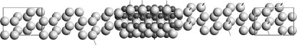
FIGURE 68.2 A device model of a thin slice of Si3N4 embedded in Si (111). The Si electrodes are marked by the unit cell “boxes,” which are repeated infinitely to the left and right, respectively. The atoms in between the electrodes form the central region, in which the entire electronic structure must be computed self-consistently. We note that there is also Si in the central region—this is necessary to provide a smooth transition from bulklike Si near the electrodes to the Si layers closest to the Si3N4, where the electronic structure is different due to interactions with the sandwiched material, and where the Si atoms even rearrange themselves geometrically to best fit the interface structure. The electron transport takes place between the electrodes, and the entire system is periodic in the plane transverse to the transport direction.
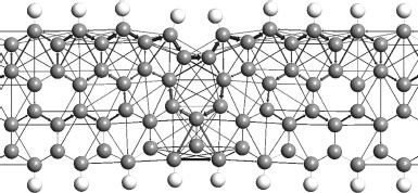
FIGURE 68.3 Transmission pathway at the Fermi level for a graphene nanoribbon with a Stone–Wales defect on one of the edges [7]. This visual way of representing the results provides an intuitive way to understand the electron transport mechanism.
As noted in the previous section, the fundamental quantity to be computed is the transmission spectrum, which is a function of the energy of the incoming electrons from the electrode. The transmission spectrum can then be integrated to give the current at the given bias, but it can also be decomposed and projected in different ways, resulting in supporting quantities that can assist in the analysis and understanding of the transport mechanisms.
Examples of such quantities are transmission eigenvalues and eigenstates, transmission pathways (Figure 68.3), current density, and the real-space density of states. All of these provide a visual image of how the electrons travel through the structure, although one has to keep in mind that the final current depends on the collective behavior of all states, integrated over wave vectors and energy.
Other quantities that provide insight are the nonequilibrium density of states (atom and orbital projected) and the complex band structures of the electrodes. The regular band structure is of course of relevance too, but the complex band structure also gives information about states in the band gap, in the case of semiconductor electrodes.
This deep-level understanding is one of the key takeaways from modeling and simulation. Although one can often achieve a good qualitative agreement between experiments and computed results, the possibility to dig deeper into the mechanism is only available in silico. This can provide far more insight about the system than can be obtained in an experiment—insight that can be used to guide new experiments in directions of most likely success, or give rise to entirely new ideas not tried before. Moreover, even if the calculations do not take all possible environmental effects into account, the simulated results provide a limit for the performance of an ideal device, thus giving an indication of the feasibility of a suggested device design. Used in this way, modeling does not replace experiments and measurements but supports and guides them.
68.4 QUANTUM-MECHANICAL DEVICE MODELING
This section will review the essential points of the models needed to compute the transmission spectrum accurately and reliably from a quantum-mechanical perspective. In summary, the crucial ingredients are
• Atomistic models—we need to describe the detailed scattering potential landscape of the central device region, with individual atomic impurities, and so on; this was already discussed above.
• Quantum models—required to accurately describe the electronic structure of ultrathin films, molecules, graphene, nanotubes; in Section 68.4.1 below, we will consider the models that are available, as well as their respective advantages and disadvantages.
• Boundary conditions—a major point that we will elaborate more on in Section 68.4.2.
• Nonlinear response—in toy models or very simple systems, it may be possible to compute the transmission spectrum at zero bias and then just extrapolate to finite bias. Experience shows, however, that in the majority of realistic systems, the transmission spectrum itself depends on the bias. Thus, it is necessary to employ methods that can treat systems in the nonequilibrium situation where a finite bias is applied across the central region. This is also closely related to the boundary conditions.
We can also point out the two single most important factors that determine the quality of the results:
• An accurate band structure (including the HOMO-LUMO gap of molecules) of the electrodes and the scattering region (see Section 68.4.2); this primarily determines the zero-bias properties of the transport system.
• A correct description of the voltage drop that occurs across the central region (see Section 68.4.3) allows for an accurate computation of the tunneling current at finite bias.
One should pay attention to the fact that the electronic structure and transport properties are not two separate quantities. They are deeply coupled since there is information extracted from the electronic structure that goes into the electrostatic model used to compute the voltage drop, and the potential distribution in turn influences the occupation of the electronic states. We therefore end up with a rather complex nonlinear problem with a higher complexity than the usual self-consistent iterative scheme used in the coupled Schrödinger/Poisson equation solvers, since the total number of carriers is not conserved in the calculation—charge can move in and out of the electrodes that are infinite reservoirs for electrons. A powerful approach for computing the occupations of the states in the central region in this situation (with or without a bias applied) is the nonequilibrium Green’s function (NEGF) formalism, which has become the standard tool for this task [3] due to its computational efficiency and numerical stability, although in principle one can also use scattering states, transfer matrices, and other methods.
For the electronic structure, however, there are a few choices, which we will discuss in the following section.
68.4.2 ELECTRONIC STRUCTURE METHODS FOR ATOMIC-SCALE DEVICE MODELING
Ab initio methods, in which we also count DFT, have the advantage of being able to describe any combination of elements without the need for predefined parameters. This is clearly of importance in cases where new materials are being developed, and in particular when materials are being combined in new ways, for example, at interfaces, where the bonding character changes from bulk to molecular. It also makes it possible to combine organic and inorganic materials.
A common concern about DFT is the issue related to obtaining a correct description of the band gap of semiconductors. For some applications, this is not really an issue—geometrical properties and total energies are often well represented by DFT. The traditionally inaccurate estimation of the band gap does however raise some questions for the electronic transport properties in some cases. Recent developments of models that allow the inclusion of the on-site Hubbard terms can however “cure” the band gap in many situations, and alleviate the problems of interface states ending up in the conduction band, rather than in the band gap, without incurring any real increase in computational effort. One can also try to use novel exchange-correlation functionals like meta-generalized gradient approximation (GGA) [8], although it may introduce nontrivial effects for, for example, layered systems that contain both metals and dielectric layers; even if the band gap of the insulator can be adjusted (cf. Figure 68.4), the metal may suffer from distortion of its band structure and a shift of the Fermi level. Thus, the Hubbard model may be preferable for device systems since it treats each chemical element individually, and can be fitted to accurate band structures—perhaps produced with meta-GGA. Screened exchange or functionals of similar nature like HSE06 may offer a third and, in many ways, better alternative, however, at the cost of a noticeable increase in the computational time.
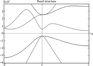
FIGURE 68.4 Band structure of germanium, computed with DFT and the TB09 meta-GGA functional in Atomistix ToolKit. Unlike for LDA or GGA, we here obtain band gaps at both the L and Γ points that agree with experiments to within 5%, and also a very reasonable effective mass for the lowest conduction band at the Γ point. Interestingly, at the L point, the conduction band effective mass is accurately estimated by basic GGA, even if the band gap comes out completely wrong.
The Slater–Koster tight-binding models are not in the same way transferable, meaning that the parameters usually have to be tailored for each specific problem. However, they do offer treatment of far larger systems than DFT [4] and give a correct band gap essentially by construction. In particular, tight-binding models often only take into account interactions between adjacent atoms, and combined with routines for operating on sparse matrices; this allows for efficient handling of even hundreds of thousands of atoms. At that scale, one is actually approaching small but realistic models of entire transistors. Also, for example, for III–V materials composed of random alloys like AlGaAs, it is necessary to use large supercells to provide statistical accuracy in terms of the material composition fluctuations; methods based on special quasirandom structures (SQS) or virtual crystal approaches attempt to provide some systematic approach to this problem, but have not been tried extensively for transport modeling yet.
An intermediate position is taken by semiempirical models such as the extended Hückel theory (EHT) [5] and DFTB [9], where a smaller number of empirical parameters are fitted to experimental results or very accurate calculations. The computational demands are smaller than for DFT, while offering a more transferable approach than tight-binding, not least thanks to the self-consistency included in the model. DFTB has the additional advantage of incorporating a repulsive potential, and thus this formalism can also take ionic movement into account, to enable geometry optimizations, molecular dynamics simulations, and calculations of reaction barriers using nudged elastic bands (NEB). As long as the geometry remains within the space covered reasonably well by the parameterization, this method can be very accurate.
In summary, as long as the model is able to correctly describe the band structure and other electronic structure properties of the system, there is no inherent additional accuracy in more complex models like DFT. Their advantage is a higher transferability; there is no need to consider different parameters for different problems. If, on the other hand, we have suitable parameters for a broad range of systems, the lower computational cost and perhaps even the better band gap description of parameterized models make them very attractive.
The main limitation for the use of semiempirical models is however the poor availability of parameters for material combinations outside certain well-established areas; in particular, there are almost no metal/semiconductor parameter sets. Precisely the same issue holds for classical potentials, which could enable even process simulations with millions of atoms for semiconductor materials. A task for the future is therefore to develop methods by which tight-binding parameters and classical potentials can be fitted to new materials and material combinations in an efficient manner, so that one can take advantage of the higher calculation speed of the simpler methods without relying on generic parameters, which may not apply to the actual system. An interesting development here are bond order potentials like reaxFF, which can describe chemical processes where bonds are formed and broken, and which have parameters for almost the entire periodic table, at least for certain types of materials [10]. Another good example of this are the EHT parameters tabulated by Cerda [11], which among others contain an excellent set of parameters for sp2-bonded carbon, that is, graphene and nanotubes. If, on the other hand, one attempts to use the “standard” carbon EHT parameters (by Hoffmann or Müller) for graphene, the results are completely disastrous, due to the fact that these parameters apply to sp3-bonded atoms. Fitting semiempirical parameters is a huge task by itself, but one of the fundamental prerequisites is an accurate DFT code that can easily be integrated with automated fitting schemes, to reduce manual labor. Thus, having a platform where different codes can be accessed through a common interface helps a lot, not just for the fitting but also for making it possible to quickly compare the accuracy of different models.
Our software package, Atomistix ToolKit® (ATK) [7], is developed with this in mind. It comprises a wide range of electronic structure models (essentially all those mentioned above), which can all be combined with an NEGF framework to compute transport properties of all possible device geometries discussed in this work.
68.4.3 ELECTROSTATICS AND BOUNDARY CONDITIONS
There is a multitude of quantum-mechanical software packages available for computing the electronic structure of atomic-scale systems. Generally, they apply to one of two types of boundary conditions: periodic structures that are infinite in three or fewer dimensions (examples include three-dimensional bulk crystals, two-dimensional graphene sheets, and one-dimensional nanotubes or nanowires), or finite structures (clusters, molecules). In a transport system, however, neither applies: although the electrodes are periodic, and are computed as such during the transport calculation, the central region is finite. Thus, a method that can combine these two geometry types is required. In addition, we must also consider the possibility of applying a potential difference between the source and drain electrodes to drive a current through the structure, as well as electrostatic gates that can modulate the current. This breaks any periodicity that might otherwise be present in the system.
Therefore, we need to use open boundary conditions in the transport direction, such that charge can flow between the source and the drain. This is where the NEGF method comes in, as it can describe a nonequilibrium distribution of electrons in the central region. As mentioned above, the entire problem must be solved self-consistently, not only for the electronic structure—as is inherent at least in DFT—but also for the charge redistribution that takes place between the electrodes, acting as reservoirs of electrons, and the central region.
The problem is highly nonlinear, and convergence can be hard to achieve unless care is taken in the mixing of algorithms and the precise way in which matrix elements are computed close to the edges of the central region. This is one of the main points where different implementations of the NEGF transport method differ the most. In ATK, we have made sure to include all possible contributions to the Hamiltonian matrix elements of the central region, also those that arise from interactions with atoms in the electrodes, the so-called spill-in terms. We have also implemented a double-contour algorithm that allows for bound states to be present in the bias window. This is crucial for the physical correctness of the model, and the ability to apply a realistically large bias to the structures.
For the electrostatic potential, we employ Dirichlet boundary conditions on the surfaces connecting the electrodes and the central region, which allow for inclusion of the finite bias directly in the boundary conditions. This requires a multigrid method, which is considerably more time-consuming than the usual fast Fourier transform (FFT) methods that can be used to solve the Poisson equation under periodic boundary conditions. For systems with periodic boundary conditions in the transverse plane, it is possible to combine FFT methods in these directions with a multigrid method in the transport direction. This makes it easy to study interface systems using a small transverse unit cell, although for 1D or 2D systems one needs to introduce vacuum padding to avoid spurious electrostatic and other interactions between the repeated copies of the system.
If, additionally, we also add one or more electrostatic gates to the device (in practice, this means a metallic region plus a dielectric layer that can screen the gate potential), the periodicity in the transverse plane is also broken, and we need to employ a full multigrid method in all directions. Recently, capabilities for including metallic and dielectric regions have been incorporated into quantum transport calculations (see for example Figure 68.5), enabling calculations of realistic transistor characteristics [4,5].
It should be noted that in these simulations, the gate electrodes and dielectric screening regions are not described atomistically, but as continuum regions without structure. This allows for a great flexibility in the design of the gates, and one can consider cylindrical wrap gates, double-gates, or single back gates without changing the methodology. We also have here a multiscale simulation, where part of the system is described on one complexity level (the device is a discrete atomic system) and another on a different one (continuum regions). This paves the way for more advanced quantum device simulators that can treat realistically large structures without the need to necessarily describe the entire device atomistically but only the relevant parts that carry the current.
A complication that possibly arises in such simulations is, however, that to mimic a realistic device geometry, it is often necessary to place the electrostatic gates at a distance from the active device region that far exceeds the dimensions of the atomic-scale features themselves. Put shortly, the simulation cell will contain a lot of inactive space (vacuum), which becomes rather costly at the atomic level, not least in terms of memory. A solution here is to introduce real-space grids based on finite-element methods (FEM). This is rather straightforward to do for methods like tight-binding where the primary real-space grid is the external potential in the Poisson equation, but decidedly harder to do for DFT where we also have to evaluate the real-space density and the exchange–correlation functional based on it [12]. It is also not clear if FEM grids actually require less memory since the description of each FEM vertex requires considerably more memory than the definition of a point in a simple, regular space grid. This is at least true as long as the total simulation volume and atom count are of the order where DFT is still reasonably manageable (less than 2000 atoms or so). For tight-binding calculations of truly large-scale structures with thousands of atoms, the balance shifts, however.
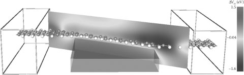
FIGURE 68.5 The self-consistent electrostatic potential of a z-shaped graphene transistor, constructed from fusing two metallic zigzag ribbons (the electrodes) and an armchair segment (the central region). The results are show for a gate potential of −1 V, at a source/drain bias of 1 V (symmetrically applied). Note how the electrostatic potential from the gate is screened by the graphene layer [5].
There are also efforts being made for handling multiterminal devices [6], but this is still an area for further research, as there are significant challenges in obtaining stable convergence and also for the computational demands in terms of time and memory. In general, such simulations are currently only tenable on supercomputer resources.
It is hopefully evident from the presentation above that there is a strong need for a new generation of device simulation tools, which can incorporate methodologies that are capable of integrating different methods, deal with combinations of metals, semiconductors as well as organic materials, and which can compute both electronic and thermal transport properties in realistic nanoscale device geometries, as well as mechanical and optical properties. Whether or not this type of modeling software will be an extension of existing TCAD tools (similar to the downscaling of the devices themselves) or part of a separate bottom-up approach remains to be seen. It is far from trivial to just add another layer of “quantum effects” that somehow correct the classical model to account for effects that occur on the nanoscale, since these effects come in so many flavors and with a huge amount of parameters. What is clear, however, is that these tools will be an essential enabling technology for the nodes ahead in the ITRS, which mentions “atomistic” or “atomic-scale” modeling at least 15 times in the latest section on Modeling & Simulation [1]. This applies not only to the far-out nodes at 10 or 5 nm but also the more imminent ones. With a deeper fundamental understanding of the processes, materials, and operation behavior of the novel devices comes improved reliability and scalability, while development speed can increase and uncertainties and risks can be reduced.
In general, the methods outlined above, whether referring to the way the geometry is optimized or the method that is used for the electronic structure calculation, have their own set of advantages and specific areas of applicability. No single method—or even code—can hope to solve all the problems. What is required is thus a simulation framework that comprises several methods. The real power, however, comes from not only having these different methods coexisting, but also making it possible to combine them, so that one can leverage the respective advantages of each methodology. This will enable true multiscale modeling that can span many orders of length and time scales. In this way, the modeling tool can deliver reliable results in a timely manner to the developer or engineer working not only with standard structures but also novel device ideas, even based on exotic combinations of materials.
It is our desire and goal to create such a framework with our simulation platform, ATK. In order for this effort to be successful in delivering a tool that is useful for solving real problems at hand, a close dialog is however needed with relevant industrial and academic partners. With this chapter, we would like to invite anyone interested to thus discuss the foundation of “nano TCAD.”
1. The International Technology Roadmap for Semiconductors (ITRS). http://www.itrs.net/.
2. S. Datta, Electronic Transport in Mesoscopic Systems, Cambridge University Press, Cambridge, 1997.
3. M. Brandbyge, J.-L. Mozos, P. Ordejon, J. Taylor, and K. Stokbro, Phys. Rev. B. 65, 165401, 2002.
4. G. Klimeck. F. Oyafuso, T.B. Boykin, C.R. Bowen, and P. von Allmen, Comput. Model. Eng. Sci. 3, 601, 2002.
5. K. Stokbro, D.-E. Petersen, S. Smidstrup, M. Ipsen, A. Blom, and K. Kaasbjerg, Phys. Rev. B. 82, 075420, 2010.
6. K.K. Saha, W. Lu, J. Bernholc, and V. Meunier, Phys. Rev. B. 81, 125420, 2010.
7. Atomistix ToolKit (ATK), http://www.quantumwise.com.
8. F. Tran and P. Blaha, Phys. Rev. Lett. 102, 226401, 2009.
9. M. Elstner et al., Phys. Rev. B. 58, 7260, 1998.
10. A.C.T. van Duin, S. Dasgupta, F. Lorant, and W. A. Goddard III, J. Phys. Chem. A. 105, 9396, 2001.
11. http://www.icmm.csic.es/jcerda/EHT_TB/TB/Periodic_Table.html
12. J. Avery, PhD Thesis, Copenhagen University, February 2011.