
Chapter 13
Hardware Attacks
The portability and versatility of Android across a diverse range of mobile hardware platforms has made it extremely successful in the mobile space, almost to the point of ubiquity. Its portability and flexibility is also one factor that's pushing Android to become the operating system of choice for other kinds of embedded systems. Android is open, highly customizable, and is relatively easy for rapidly developing visually appealing user interfaces. This is especially true when compared to previous industry standard options, such as bare-bones embedded Linux and real-time or proprietary operating systems. As the new de facto standard for a variety of new kinds of embedded devices, Android is on e-readers, set-top entertainment systems, airline in-flight entertainment systems, “smart” televisions, climate control systems, and point-of-sale systems. (And that's just to name a few that we've personally poked at.) With Android powering these kinds of devices, we'd be remiss to not at least address some simple techniques for attacking and reverse engineering these kinds of devices' hardware.
As an attack vector, physical access to hardware is generally viewed as “game over” and low threat from traditional risk and threat modeling perspective. However, in many cases “physical” techniques can be employed to perform vulnerability research that has greater impact. For example, consider a connection to an unprotected debug port on a router or switch. With proper access, this would allow an attacker the freedom to find embedded encryption keys or remotely exploitable vulnerabilities. Physical access to the device also means that an attacker can remove chips to reverse engineer them. These results can have wider impact than the few devices that were sacrificed during the research. This chapter discusses some simple tools and techniques intended to lower the barrier to entry of hardware focused embedded device security research. With physical access to a target device you can use these simple techniques to either obtain the software it contains or to attack software via hardware interfaces. After you've vaulted the hardware hurdle, many software-based exploitation and reverse-engineering techniques apply again. This might include using a disassembler to hunt for vulnerabilities in the firmware or discovering a proprietary protocol parser for data arriving on a hardware interface like Universal Serial Bus (USB). These techniques are very simple and do not dive into hardcore electrical engineering topics. Although most of these techniques—such as debugging, bus monitoring, and device emulation—are relatively passive, a few are slightly more destructive to the target device.
Interfacing with Hardware Devices
The first thing you might want to do as a reverse engineer or vulnerability researcher is to enumerate the ways you can interface (on a physical level) with the target device. Are there any exposed interfaces on the device? Are there ports or receptacles for things like USB or memory cards? We'll discuss some of these familiar interfaces later in this chapter, but for now this section discusses some of the things you might encounter after you pop open a device's casing and are looking at its printed circuit board (PCB). Before we go into examples and test cases, the section describes a bit about the most common hardware interfaces found in devices.
UART Serial Interfaces
Universal Asynchronous Receiver/Transmitter (UART) interfaces are by far the most common interface for diagnostic and debug output from embedded devices. UART Serial interfaces may implement one of a handful of communication standards (RS-232, RS-422, RS-485, EIA, and so on). These communication standards merely dictate details such as the characteristics of signals (i.e., what different signals mean — start transmitting, stop transmitting, reset the connection, and so on). These standards also dictate things like timing (i.e., how fast data should be transmitted) and in some cases the size and description of connectors. If you want to learn more about the different flavors of UART, the Internet is a great source of these very old and well-documented standards. For now, however, the most relevant point is that these kinds of interfaces are extremely common in embedded devices.
Why is UART so common? It offers a simple way to transfer data directly to and from controllers and microprocessors without needing to go through intermediary hardware that's too complex to be cheaply included in a microprocessor. Figure 13.1 shows a UART interface that connects directly into a central processing unit (CPU).
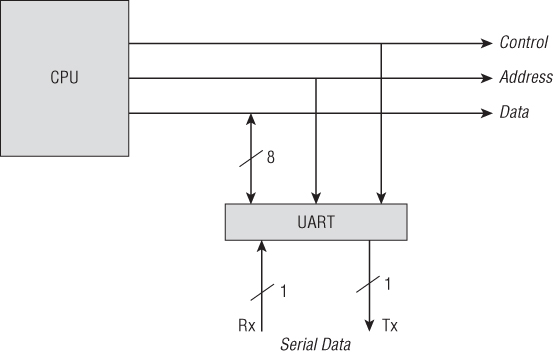
Figure 13.1 UART Serial directly connected to a CPU
UART Serial interfaces long pre-dated dedicated video cards, keyboard/mice ports, and network interface cards as a primary way to interface with computers. Many of the earliest computer systems ran without a keyboard, mouse, monitor, or video output. Instead, the only control interface was a serial port that a user would connect to a dedicated “dumb terminal” (such as Wyse). For many years this was the most common way to access the command-line console of a computer: via a UART serial port. In fact, many modern Unix concepts stem from these early origins. For example, many Unix and Linux users are familiar with the concept of their terminals running on a TTY. This term itself is from an era when interfacing with Unix systems was done via a serial connection to a TeleTYpe Writer (hence the abbreviation TTY).
UART serial interfaces can come in many different flavors but the simplest can be implemented with as little as three or four connecting wires. The simplicity of UART means it is a very cheap and lightweight to implement in a circuit design. As such, UART consoles can be found in virtually every embedded system, often getting embedded directly into System-on-Chip (SoC) products created by original equipment manufacturers (OEMs).
On embedded systems, such as set-top boxes, the video output is generally dedicated entirely to the high-level user interface. Additionally, devices like these may have limited user input, such as a dedicated remote. In these circumstances, a market-ready product leaves few options for lower-level debug functionality. Therefore, one can envision how developers might find a UART serial console (hidden within the device) extremely useful for debugging and diagnostics. Indeed many consumer-grade products leave these interfaces exposed and enabled.
What Does an Exposed Serial Interface Mean?
Whether you have the ability to directly interface with the embedded operating system (OS) using an exposed serial console or the ability to intercept, view, tamper with, or generate data on any of these intra-chip conversation paths, the effect is the same: more attack surface. As you read in Chapter 5, the size of a target's attack surface is directly proportional to how much it interfaces with other systems, code, devices, users, and even its own hardware. Being aware of these interfaces broadens your understanding of the attack surface of a whole host of devices, and not just those running Android.
Exposed UART on Android and Linux
It is common in embedded Android-based systems to find exposed UART serial ports that (when properly connected) will allow console access directly to the underlying operating system. As discussed throughout this book, the common way to interface with Android is via Android Debug Bridge (ADB). However, it is quite common for Android-based embedded systems (that have exposed UART) to have been compiled with these kernel compile-time options:
CONFIG_SERIAL_MSM
CONFIG_SERIAL_MSM_CONSOLE
Then generally the boot loader, such as uBoot and X-Loader, will pass the kernel the serial port configuration options via a boot-time option such as the following:
"console=ttyMSM2,115200n8"
In this case, all “stdout,” “stderr,” and “debug” prints are routed to the serial console. If the device is running Android or standard Linux and login
With these interfaces, you can generally watch the device boot, print debug, and diagnostic messages (think syslogdmesg
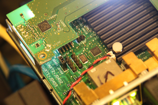
Figure 13.2 Set-top box pinouts
When connected to the appropriate pins on the circuit board, the few leads shown in Figure 13.2 could be used to access a root shell on the embedded Android operating system. The exact same technique, when applied to a popular Broadcom-based cable modem, revealed a customized Real-time operating system. Although there was no interactive shell on the UART of the Broadcom, when services on the device's Internet Protocol (IP) address were fuzzed, stack tracks displayed on the UART, which ultimately informed the exploitation process. The UART pins for this device are pictured in Figure 13.3.
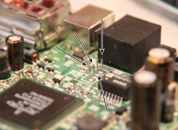
Figure 13.3 Comcast Broadcom pinouts
These are just two simple examples from our own research. This same vulnerability, an unprotected UART, has been found on many more devices privately. The Internet is rife with blog posts and information security presentations based entirely on exposed UARTs, such as femtocell hacking, OpenWRT Linksys hacks, cable modem vulnerabilities, and satellite dish hacks.
So how do you go about finding these hardware interfaces? How might you discover which pins do what? You will learn some simple techniques and tools for how to do this in the “Finding Debug Interfaces” section later in this chapter. First, though, you should have some background on the other types of interfaces you might also encounter so you can differentiate between them.
I2C, SPI, and One-Wire Interfaces
The aforementioned UART serial interfaces are generally used when a human needs to interactively interface with the machine. There are, however, even simpler serial protocols that can be found in virtually every embedded device. Unlike UART, these serial protocols arose out of a need for the integrated circuits (ICs or “chips”) in a given circuit to communicate with each other. These simple serial protocols can be implemented with very few pins (in some cases, just one pin!) and as such allow for circuit designers to simply form the equivalent of local area networks on the circuit board so that all the chips can speak to one another.
The most common of these simple serial protocols are I2C and SPI. I2C or I2C (pronounced “I squared C”) comes from its expanded abbreviation which is IIC (Inter-Integrated Circuit). SPI comes from Serial Peripheral Interface bus, and One-Wire (1-Wire) derives its name from the fact that it only requires one wire or one contact to provide power and the communication path.
Before we continue discussing how ubiquitous and common these serial protocols are in ICs, it is important to point out that not every trace on a PCB between components can be assumed to be carrying serial data. Unfortunately, it is not that simple. Many ICs will also share data and interface with other ICs the old-fashioned way — by simply changing the state of a series of pins (high or low voltage relative to some fixed norm representing binary 1 or 0 respectively). Generally pins such as these are referred to as GPIO which stands for general purpose input/output.
Some pins carry analog signals and some digital. So in those cases you would likely need to understand the protocol that the IC uses to communicate with the outside world. Generally, that can be found by simply reading the manual for that IC or by skimming through the specifications sheet for the pinouts. (This quickly gets into the realm of detailed electrical engineering, which is beyond the scope of this book.)
That said, rarely do you need to go into this level of detail thanks to the ubiquity of these simple serial protocols. Because these simple serial protocols require much less complexity than UART, they can be easily and inexpensively embedded into virtually any IC capable of outputting digital data to a few of its pins. These serial protocols are commonly found in the wild implemented in ICs that do virtually anything, including:
- Tilt/Motion detection (accelerometers)
- Clocks
- Stepper motors
- Servos
- Voltage regulators
- A/D (analog-to-digital) converters
- Temperature monitors
- Data storage (EEPROM)
- LCD/LED displays
- GPS Receivers (Global Positioning Satellites)
Because virtually every manufacturer wants its ICs to be easy to interface with, I2C and SPI are the standard for simple digital communication. For example, I2C serial communication is how Nintendo Wii controllers communicate. The cable that connects the Nintendo controller to the Nintendo unit uses it. SPI and I2C are how most notebook batteries report their remaining charge to software on the notebook. Often the logic for regulating the temperature, output, and state of a notebook battery is implemented in software on the laptop, which then controls the battery via the I2C bus.
Every VGA, DVI, and HDMI cable/device has dedicated I2C pins that are used as a rudimentary communication channel between the device and the video card (or controller). Figure 13.4 depicts the pins involved in the I2C interface of common VGA, HDMI, and DVI connectors.
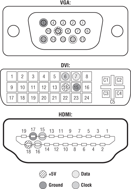
Figure 13.4 VGA-DVI-HDMI I2C pins
When you plug a new monitor into your computer and the computer reports the exact make and model, this is because it received that information from the monitor itself across two dedicated I2C pins in the video cable.
Even MicroSD and SD cards transfer all their data over an SPI serial bus! That's right, your memory card talks to your computer via SPI, a simple and flexible old-school serial protocol. Figure 13.5 shows the specific pins on the MicroSD and SD connectors that are involved in SPI communications.
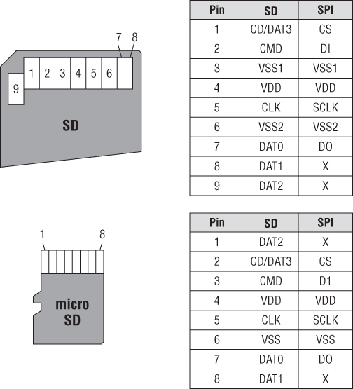
Figure 13.5 MicroSD and SD cards use SPI
With these simple examples, hopefully now you've realized how truly ubiquitous these serial protocols are. Perhaps the most relevant example of where these protocols are found is that I2C is commonly found between the application processor and the baseband processor in smartphones. In fact, by spying on the communication crossing the I2C bus, George Hotz (aka GeoHot) was able to create the first iPhone jailbreak. By spying on the I2C data destined for the built-in power controller in MacBook batteries, Dr. Charlie Miller was able to reverse engineer how Apple laptop computers controlled their power sources.
JTAG
JTAG has become a bit of a loaded buzzword in the security world. We've probably all been guilty of tossing it around without understanding what it really means. This is because the concept seems so simple and familiar: It's a way to debug a chip from a separate computer. But the reality is a bit different than you might think.
By now you've reviewed how simple serial protocols are used by integrated circuits to talk to each other and peripherals. You've also read how these serial interfaces are often used by developers to interface interactively with the operating system and boot loaders or to receive debug output from them. All this interactivity and output can be very useful, but there is another key bit of functionality that an embedded developer would likely need for successful development and deployment: debugging.
UART relies on dedicated code executing on the embedded device to handle the interface (that is, a shell, an interactive boot loader, and so on). How might an embedded developer gain visibility into what the processor is doing without anything executing on the processor — especially before the processor has begun execution or while the processor is paused? On embedded systems, it is not merely as simple as installing a software debugger. For example, what if your target is running a real-time operating system in which there is no concept of user-space or multiple processes? If your debug target is something like an RTOS (real-time operating system) or a bare-metal executable in which there is one single executable image running, there is really only one other alternative: hardware debug interfaces such as JTAG.
The standards and specifications are beyond the scope of this chapter, but it is important that you know that JTAG refers to the IEEE standard 1149.1 “Standard Test Access Port and Boundary Scan Architecture.” This standard came into existence thanks to a body called the Joint Test Action Group (JTAG) composed of OEMs, and developers. JTAG is named after that group and not the standard.
This is an important point because it sets the stage for misconceptions about the technology and also its varied uses. It's important to keep in mind that JTAG is a well-defined standard, but it does not define how software debugging is done. It is proof of how it is an often cited but poorly understood concept in developer and information security communities. Once these concepts are properly understood, they enable developers and researchers to debug and intrusively access embedded software to find vulnerabilities.
The JTAG Myth
Perhaps the greatest misconception about JTAG is that it is highly standardized with regard to software debugging. The standard defines a bidirectional communication path for debugging and management. In this case, the word “debugging” does not have the same meaning as software people are familiar with: watching a program execute. Instead it was initially more focused on “debugging” in the electrical engineering context: knowing if all the chips are present, checking the state of pins on various chips, and even providing basic logic analyzer functionality. Embedded in the lower-level electrical engineering debug functionality is the ability to support higher-level software debugging functionality. What follows is an explanation as to why this is.
In reality, JTAG is a more general term to describe a feature of a chip, IC, or microprocessor. With regard to firmware and software debugging, it is similar to referring to the transmission of a vehicle. The high-level concept is fairly easy to understand. The transmission changes the gears of the car. However, the intricacies of how a car's transmission is constructed changes with each car manufacturer, which in turn matters immensely when servicing it, dismantling it, and interfacing with it for diagnostics.
As a standard, JTAG sets forth guidelines for these lower-level features and functionality as a priority but does not specify how software debugging protocol data should be formed. From a software perspective, many JTAG on-chip debugger (OCD) implementations do tend to work alike and provide a consistently minimal amount of functionality. Single stepping, breakpoints, power resets, watch-points, register viewing, and boundary scanning are among the core functionality provided by most JTAG implementations. Also, the labels that denote the JTAG pins in a device (for the most part) use the same notation and abbreviations. So even from a functional standpoint it is easy to misunderstand what exactly JTAG is.
The JTAG standard defines five standard pins for communication, which you may or may not see labeled on the silkscreen of a PCB or in the specifications for chips and devices:
- TDO: Test Data Out
- TDI: Test Data In
- TMS: Test Mode Select
- TCK: Test Clock
- TRST: Test Reset
Figure 13.6 shows several standard JTAG headers that are used in various devices.
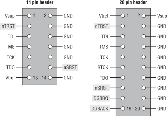
Figure 13.6 JTAG header diagram
The pin names are basically self-documenting. A software person may immediately assume that JTAG, as a standard, defines not only the pins but also the communication that happens across those pins. This is not so. With regard to software/firmware debugging, the JTAG standard simply defines that two pins be used for data transmission:
- TDO: Test Data Out
- TDI: Test Data In
It then goes on to define some commands and the format of commands that should be transmitted over those pins (for broader JTAG functionality) but does not specify what kind of serial protocol should be used for that data. JTAG also specifies different modes for any device connected to the JTAG bus:
- BYPASS: Just pass data coming in on TDI to TDO
- EXTEST (External test): Receive command from TDI, get external pin state information, and transmit on TDO
- INTEST (Internal test): Get internal state information and transmit on TDO; also do “other” user-definable internal things
For all software/firmware debugging communication that happens across the data pins of a JTAG interface, it is up to the vendor to implement in the user-definable INTEST mode of JTAG communication. And indeed that's where all the software debugging stuff that we, as reverse engineers and vulnerability researchers, care about is contained. All software and firmware debugging information is transmitted between a chip and a debugger and is done so independent of the JTAG specification by making use of the “user definable” INTEST portion of JTAG specification.
Another common misconception is that JTAG is a direct connection to a single processor or that it is specifically for the debugging of a single target. In fact, JTAG grew out of something called boundary scanning; which is a way to string together chips on a PCB to perform lower-level diagnostics, such as checking pin states (EXTEST mentioned earlier), measuring voltages, and even analyzing logic. So JTAG is fundamentally meant to connect to more than just a single chip. Figure 13.7 shows how several chips could be connected together to form a JTAG bus.
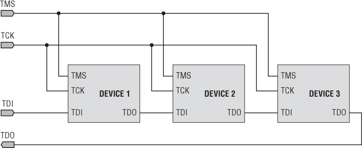
Figure 13.7 Chaining on a JTAG Bus
As such, the JTAG specification has one master and a number of slaves. Therefore it allows for daisy chaining multiple processors in no particular order. The master is often the debugger hardware (such as your PC and JTAG debugger adapter) or diagnostic hardware. All the chips on the PCB are generally slaves. This daisy-chaining is an important thing to note for reverse engineers because often a JTAG header on a commercial product will connect you to the core processor as well as to peripheral controllers, such as Bluetooth, Ethernet, and serial devices. Understanding this simple fact saves time and frustration when configuring debugger tools and wading through debugger documentation.
The JTAG specification sets no requirement for device order. Understanding the fact that slaves never initiate communications makes using and examining JTAG devices much easier. For example, you can assume with certainty that your debugger will be the only “master” in the chain. Figure 13.8 shows an example of how communications paths would look with a master connected.
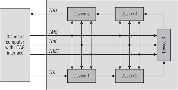
Figure 13.8 JTAG daisy-chaining
Hopefully you now see that JTAG was predominantly for electrical engineering debugging. As software developers, reverse engineers, and vulnerability researchers, what we care about is debugging the software or firmware on a device. To that end, the JTAG specification loosely designates pins and labeling for use in software/firmware debugging. That data is transmitted with serial protocols!
The JTAG specification does not specify which serial protocol is to be used or the format of the debugging data transmitted. How could it if JTAG is to be implemented on virtually any kind of processor? This fact is at the heart of the implementation differences and indeed the core misconception about JTAG in developer communities.
Each JTAG implementation for firmware and software debugging can use different data formats and be different even down to how it is wired. As an example, Spy-Bi-Wire serial communication is the transport used in the JTAG implementation for Texas Instrument's MSP430 series of microprocessors. It uses only two wires where the traditional JTAG implementation might use four or five lines. Even though a header on a MSP430 target may be referred to as JTAG or have JTAG labels on the silkscreen of the PCB, the serial pins of the JTAG connection use Spy-Bi-Wire. Therefore a hardware debugger needs to understand this pin configuration and serial protocol to pass the data to a software debugger. (See Figure 13.9.)
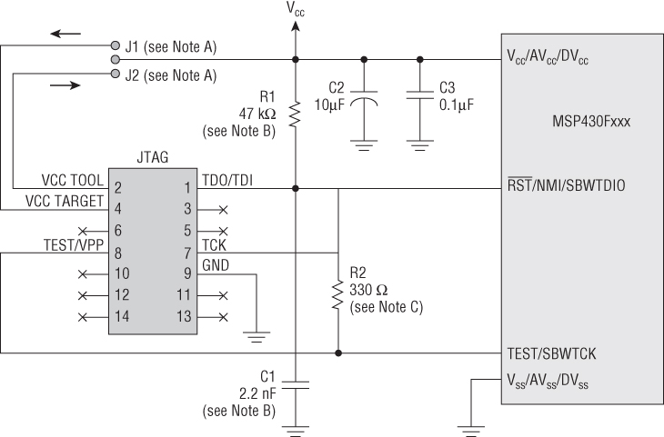
Figure 13.9 Spy-Bi-Wire comparison
In Figure 13.9, you can see the traditional 14-pin JTAG header on the left, of which only two lines are used for data by the Spy-By-Wire MSP430 processor on the right (RST/NMI/SBWTDIO and TEST/SBWTCK). In addition to the physical wiring being different, sometimes the actual wire-line protocol (the debugger data flowing across the TDO and TDI pins inside the INTEST user-defined sections) can be different. Consequently, the debugger software that speaks to the target must also be different. This gave rise to a number of different custom debugging cables, debugging hardware, and debugger software for each individual device!
But don't be intimidated! We only explain this as background information. We offer it to you to help avoid the inevitable disappointment that would come when sitting down to try JTAG with the incorrect assumption that JTAG is a highly standardized and universal debugging silver bullet. You need an understanding of JTAG so that you know what tools to get and why.
JTAG Babel Fish
Fortunately, there are a handful of companies that recognized the need for a Babel fish (a universal translator) to help make sense of all the different JTAG implementations. Vendors like Segger, Lauterbach, and IAR have created PC-based software and flexible hardware devices that do all the magic translation so that you can use their single devices to talk to different JTAG-enabled hardware devices.
JTAG Adapters
These universal JTAG debuggers are very much like universal television remotes. The vendors that create these debuggers publish long supported device lists that catalog hundreds or thousands of IC/microprocessor serial numbers that a given JTAG debugger is known to reliably support. Also much like television universal remotes; the more features, programmability, and supported devices a debugger can support, the higher the cost. This is an important thing to keep in mind if you are purchasing for a specific project. Be sure that your target is supported by the JTAG debugger you are purchasing.
Perhaps the most popular JTAG debugger, and the one most readers will find more than adequate, is the Segger J-Link, shown in Figure 13.10. The relatively low cost and extremely long list of supported devices makes it the go-to JTAG debugger for developers. There are different models of J-Link, varying in feature sets, but the core universal debugger functionality is common to them all.
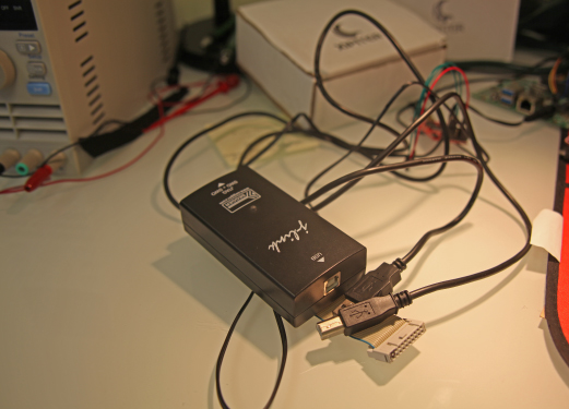
Figure 13.10 Segger's J-Link
To begin debugging, you simply plug the J-Link hardware into your computer via USB and then attach the J-Link box to your target chip via a ribbon cable or jumpers that you wire yourself (which is covered in the “Finding JTAG Pinouts” section later in this chapter). The Segger software then speaks to the J-Link device giving you control of the hardware device. The J-Link software will even act as a GNU Debugger (GDB) server so that you can debug a chip from a more familiar GDB console! Figure 13.11 shows GDB attached to the Segger J-Link's debugger server.
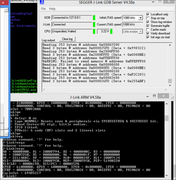
Figure 13.11 Segger J-Link and GDB screenshot
Although the J-Link is the most popular debugger, there are more industrial debuggers, like those made by Lauterbach, that are highly advanced and boast the most device support. Lauterbach's debuggers are pretty astounding but they are also prohibitively expensive.
OpenOCD
Another commonly discussed JTAG solution is OpenOCD (Open On Chip Debugger). Unlike the previously mentioned commercial tools which bundle all the software and hardware you need to immediately start working with JTAG on a device, OpenOCD is merely an open-source piece of software. The mission behind OpenOCD is to support a range of JTAG adapters and target devices (meaning the chip you are attempting to debug) that are then accessed from a standard GDB debugger interface (or any interface capable of talking to a GDB server).
Remember, the JTAG adapter itself handles all the signaling to the chip and then translates that to a PC via a USB, serial, or parallel port connection. But then a piece of software needs to speak the wire-line protocol to understand and parse that protocol and translate it into something a debugger can understand. OpenOCD is that software. In commercial solutions, both this software and the adapter hardware are bundled together.
OpenOCD is commonly used with JTAG adapters that don't include software such as the Olimex adapters, the FlySwatter, the Wiggler, and even the Bus Pirate (which is covered for other purposes later in this chapter in the “Talking to I2C, SPI, and UART Devices” section). OpenOCD even works with many commercial JTAG adapters such as the Segger J-Link.
If you are well informed about a target's pinouts, your JTAG adapter is well supported, your wiring is correct and reliable, and you've configured OpenOCD for all of these issues, using OpenOCD can be fairly simple. Installing it can be as easy as downloading it using apt-get or other application downloaders. When you have it, you merely launch OpenOCD as a command-line tool, as shown in the following code:
[s7ephen@xip ˜]$ openocd
Open On-Chip Debugger 0.5.0-dev-00141-g33e5dd1 (2010-04-02-11:14)
Licensed under GNU GPL v2
For bug reports, read
        http://openocd.berlios.de/doc/doxygen/bugs.html
RCLK - adaptive
Warn : omap3530.dsp: huge IR length 38
RCLK - adaptive
trst_only separate trst_push_pull
Info : RCLK (adaptive clock speed) not supported - fallback to 1000 kHz
Info : JTAG tap: omap3530.jrc tap/device found: 0x0b7ae02f (mfg: 0x017,
part: 0xb7ae, ver: 0x0)
Info : JTAG tap: omap3530.dap enabled
Info : omap3530.cpu: hardware has 6 breakpoints, 2 watchpoints
This chapter skips a bit of configuration, such as creating/editing the main openocd.cfg
[s7ephen@xip ˜]$ telnet localhost 4444
Trying 127.0.0.1…
Connected to localhost.
Escape character is '^]'.
Open On-Chip Debugger
>
When connected with OpenOCD, there is a very comfortable online help for the CLI that will get you started:
> help
bp                        list or set breakpoint [<address> <length> [hw]]
cpu                       <name> - prints out target options and a comment
                          on CPU which matches name
debug_level               adjust debug level <0-3>
drscan                    execute DR scan <device> <num_bits> <value>
                          <num_bits1> <value2> …
dump_image                dump_image <file> <address> <size>
exit                      exit telnet session
fast                      fast <enable/disable> - place at beginning of
                          config files. Sets defaults to fast and dangerous.
fast_load                 loads active fast load image to current target -
                          mainly for profiling purposes
fast_load_image           same args as load_image, image stored in memory -
                          mainly for profiling purposes
find                      <file> - print full path to file according to
                          OpenOCD search rules
flush_count               returns number of times the JTAG queue has been
                          flushed
ft2232_device_desc        the USB device description of the FTDI FT2232
                          device
ft2232_latency            set the FT2232 latency timer to a new value
ft2232_layout             the layout of the FT2232 GPIO signals used to
                          control output-enables and reset signals
ft2232_serial             the serial number of the FTDI FT2232 device
ft2232_vid_pid            the vendor ID and product ID of the FTDI FT2232
                          device
gdb_breakpoint_override   hard/soft/disable - force breakpoint type for gdb
                          'break' commands.
gdb_detach                resume/reset/halt/nothing - specify behavior when
                          GDB detaches from the target
gdb_flash_program         enable or disable flash program
gdb_memory_map            enable or disable memory map
gdb_port                  daemon configuration command gdb_port
gdb_report_data_abort     enable or disable reporting data aborts
halt                      halt target
help                      Tcl implementation of help command
init                      initializes target and servers - nop on subsequent
                          invocations
interface                 try to configure interface
interface_list            list all built-in interfaces
irscan                    execute IR scan <device> <instr> [dev2] [instr2]
Notice the similarities between this interface and the J-Link Commander interface.
When attempting to attach a JTAG adapter to a commercial product, you often don't have a standard or labeled JTAG pinout. You may also not know if the JTAG port is enabled. For these reasons, deploying OpenOCD against an unknown or commercial target can be fraught with peril or frustration because you have many independent variables such as the following:
- Is JTAG even active on the target device?
- What are the pinouts (that is, where are TDI, TDO, TCK, TRST, and TMS) ?
- I know the correct pinouts from the target, but are the jumpers and connectors I connected working properly?
- Is OpenOCD talking to the adapter properly via the right adapter driver?
- Is OpenOCD parsing the wire-line protocol for this target device properly via the correct interface transport?
- This exact target device model number is similar to the target I declared in OpenOCD, but it is not an exact match. Does that matter for this to work?
For all these reasons, using a commercial JTAG interface (like the Segger) with a clearly specified supported adapter list can save a lot of time and heartache. Because commercial JTAG interfaces come bundled with all the supporting software, the process is much smoother. Should you choose (or be required) to use OpenOCD, the next best thing to try is to obtain an evaluation kit for the chip that you are targeting.
Evaluation Kits
Evaluation kits are the standard way that engineers and designers find the right products for their systems. Virtually every commercial processor and controller will have an evaluation kit created by the manufacturer. They are often very low cost, ranging from free to $300 (many are about $100). In general, it behooves manufacturers to make evaluation kits cheap and accessible for people that might be developing products that use their processors.
Some manufacturers even go so far so to provide reference designs that bundle the Gerber files (the 3D model and wiring specifications) of the evaluation kits themselves along with the Bill Of Materials (BOMs) so that embedded engineers can quickly manufacture their own products without building a whole PCB around the processor from scratch. In this way, evaluation kits can also be immensely useful to reverse engineers and vulnerability researchers. Figure 13.12 shows the STMicro ARM development kit.
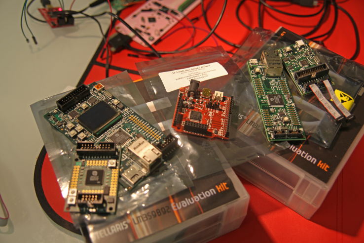
Figure 13.12 STMicro ARM development kit
The primary way that these evaluation kits are useful to reverse engineers is with regard to debuggers. The evaluation boards contain all that is needed for a developer to debug, program, and interface with a processor. They may also provide any specifications about security features of the processor that might've been employed by the manufacturer to protect the product.
You can use the evaluation kits as a control environment to test your debugging setup with software like OpenOCD. By building this kind of control environment you can test your debugger setup under ideal conditions to eliminate some of the independent variables discussed earlier. Having eliminated those, you can be confident that your debugger setup should work if your wiring is correct (to the target) and the device has JTAG enabled.
Finally Connected
After you have a debugger device connected to your target chip, either by a programming header or hand-wired connections, the debugger software notifies you that the debugger device is successfully connected to the target. In the case of the Segger J-Link, you can begin using GDB against the target immediately as shown in Figure 13.13.
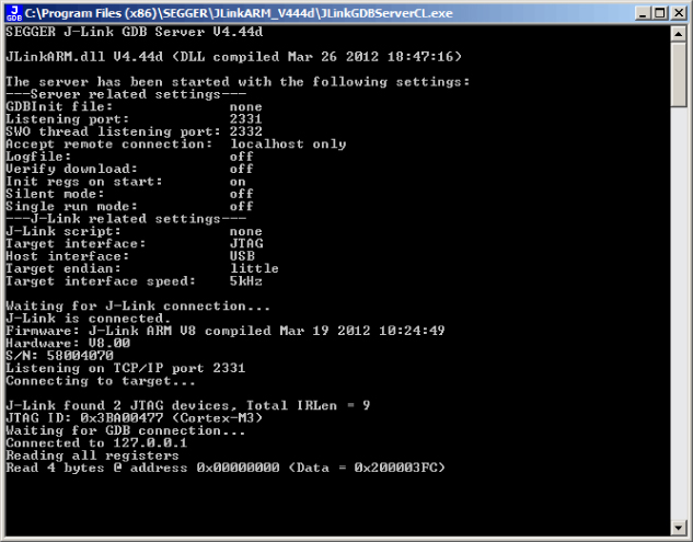
Figure 13.13 J-Link debugging the STM32 ARM devkit
Finding Debug Interfaces
Now that you have had an overview of the kinds of interfaces you might encounter (and how they work), you need to know what to do when you suspect you've found one. How do you know which pins do what? How do you get those pins connected to your tools? There are a number of tricks and tools that you may deploy to assist with making determinations about protocols and formatting.
This section lists several simple tools that you can use to identify and talk to all the interfaces we've discussed so far in this chapter (JTAG, I2C, SPI, UART, and so on). Later sections of this chapter discuss how you can connect and interface with these tools in more detail.
Enter the Logic Analyzer
Perhaps the most useful tool for determining what a pin is used for is a logic analyzer. These devices have a rather intimidating name, especially for software people, but in reality they are very simple. These devices just show you what is happening on a pin. You connect a probe from the device and if there is data being transmitted on a pin it shows you the square wave of that data and even attempts to decode it for you using a number of different filters.
Traditional logic analyzers were a bit more complex, but new generations of them connect to computer-based applications that eliminate the esoteric nature of these devices. These kinds of logic analyzers themselves have no user interface on the device itself and instead are controlled entirely by user-friendly and intuitive computer-based applications. One such device is the Saleae Logic Analyzer, shown in Figure 13.14.
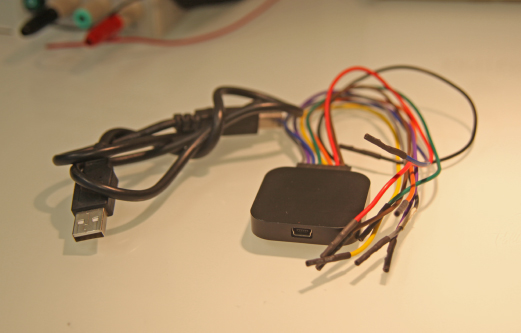
Figure 13.14 Saleae Logic Analyzer
Using the Saleae, you can connect the color-coded electrodes to pins on your target device, which enables using the software application (that receives data from the Saleae via USB) to capture activity. The results are displayed in the interface corresponding to the color of the pins of the electrodes, as shown in Figure 13.15.
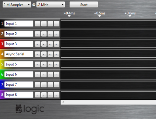
Figure 13.15 Saleae Logic Analyzer in action
As if this was not useful enough for the layperson, Saleae included a bunch of other useful functionality in the application. For example, filters attempt to decode a captured data stream as a bunch of different types such as I2C, SPI, and asynchronous serial (UART) at varying baud rates. It will even attempt to identify baud rates automatically. Figure 13.16 shows the filters commonly supported by the Saleae software.
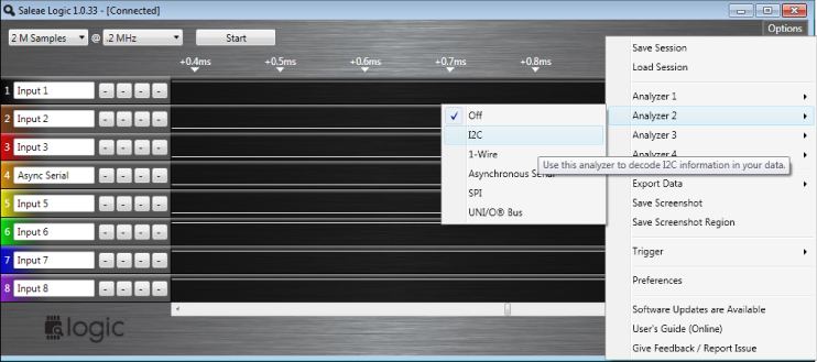
Figure 13.16 Saleae Logic Analyzer filters
These filters act much like Wireshark's protocol dissectors, allowing you to quickly view the captured data as if it were being parsed as different formats. The Saleae interface even overlays the byte encoding on the square wave form in the interface, as shown in Figure 13.17.
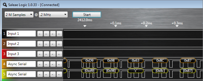
Figure 13.17 Saleae Logic Analyzer byte display
From this, you can generally immediately identify a UART signal (if not by the filters then by eye) as most UART connections are used for transmission of ASCII text.
Lastly, Saleae exports this decoded data as a binary file (for you to parse yourself) or as a comma-separated value (CSV) file with some metadata included (such as timing, pin number, etc.). This is very useful for further analysis or logging purposes.
Finding UART Pinouts
Finding UART pinouts is crucial, as UART is often used as a means to transmit debug output or to provide shells or other interactive consoles to a developer. Many production-grade products go to market not only with these interfaces active, but with the pins overtly exposed. In 2010 and 2011, Stephen A. Ridley and Rajendra Umadras demonstrated this fact in a series of talks in which they discussed a specific brand of cable modem being distributed by the home Internet service providers in the New York City metropolitan area. This series of home cable modems used a Broadcom BCM3349 series chip (specifically the BCM3349KPB) for which the four UART pins were exposed on the PCB in the small four-pin header shown in Figure 13.18.
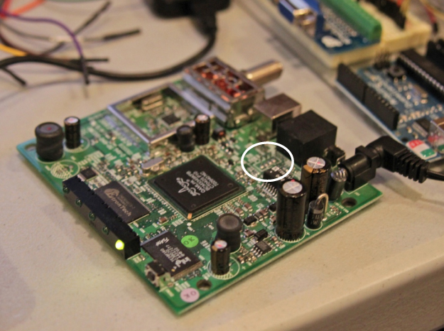
Figure 13.18 Broadcom BCM3349 4-pin header
In this case, there was little knowledge about what the pins on that header were or what they were responsible for. As a precautionary measure, a voltmeter was first connected to those pins as shown in Figure 13.19.
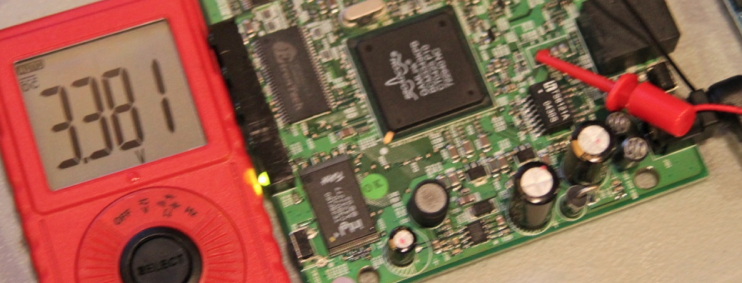
Figure 13.19 Broadcom BCM3349 voltage test
This was done to be sure that they didn't carry a voltage that would burn the analysis equipment. Additionally, the pin that carried no voltage would likely be the ground pin.
The presence of 3.3 volts, as shown in Figure 13.19, generally (but not always) implies that the target pin is used for data as most supply voltages (or lines used exclusively to power devices and not transmit data) are around 5 volts. This was a first indication that these pins might have serial data.
Next, the Saleae was connected to each pin, with each electrode connected to the pin in question. In the Saleae user interface, the color of each graph area corresponds directly to the color of each electrode on the physical device, which makes referencing it very simple. Recording data from the Saleae was started while power cycling the cable modem. The prevailing assumption was that the cable modem would likely output data during its boot sequence as the device powered on. After several recordings of boot sequences, the square waves shown in Figure 13.20 were observed on the pins.
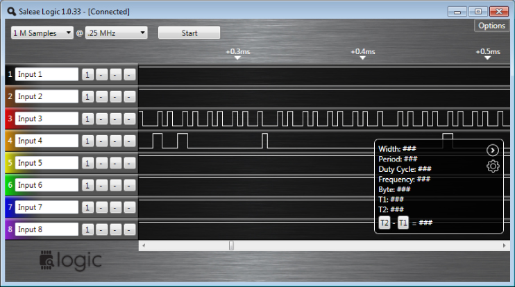
Figure 13.20 Broadcom BCM3349 Saleae pin test
The regularity of the square wave on Input 3 (which was red) indicated that the pin that the red electrode was connected to was likely a clock pin. Clock pin signals generally accompany data signals. They are the metronome to which the sheet music of data is played. They are important for the recipient to know the timing of the data it is receiving. The regularity of that square wave and subsequent irregularity of the adjacent input (Input 4) indicate that both a clock and data pin have both been observed simultaneously.
Using the Saleae functionality further, this hypothesis was tested by running the captured square waves through some of the built-in filters or analyzers.
After this Analyzer has run, it overlays the suspected byte values for each corresponding section of the square wave, depicted in Figure 13.21. It will also display the suspected baud rate.
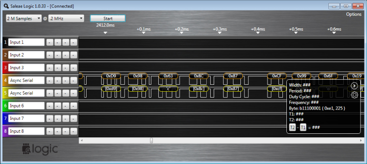
Figure 13.21 Broadcom BCM3349 Saleae Bytes
This data was output to the computer's file system as CSV data and then cleansed using a simple python script like the following:
#!/usr/bin/env python
import csv
reader = csv.reader(open("BCM3349_capture.csv", "rb"))
thang = ""
for row in reader:
    thang = thang+row[1]
thang = thang.replace("\r", "x0d")
thang = thang.replace("\n", "x0a") #clean up Windows CR/LF
thang = thang.replace("''","") #Cleanse Saleae CSV output quotes
#print thang
import pdb;pdb.set_trace() # drop into an "in scope" Python interpreter
Executing this Python script enables you to view the CSV data and manipulate it interactively from a familiar Python shell. Printing the variable thang
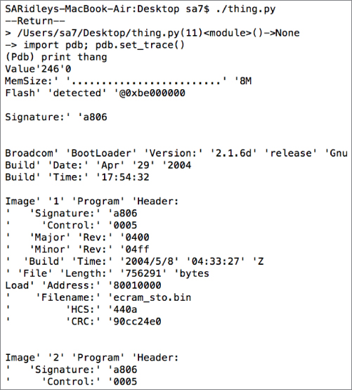
Figure 13.22 Broadcom BCM3349 bootloader
As you can see, the data captured across those overt pins is in fact boot messages from the device. The device goes on to boot a real-time operating system called eCos. The researchers that presented this technique went on to explain that the cable modem was also running an embedded webserver that they fuzzed. Stack-traces of the crashes caused by fuzzing were printed on the UART serial port shown in Figure 13.23. This information assisted in exploitation of the device.
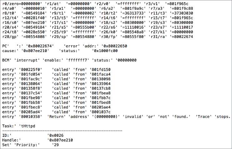
Figure 13.23 Broadcom BCM3349 crash
Finding SPI and I2C Pinouts
The process of finding SPI and I2C devices is similar to that of finding UART. However, SPI and I2C are generally used locally on the PCB to pass data between chips. As such, their functionality and usability can make them a bit different to identify. However, they will occasionally leave the PCB and be used for peripherals (often proprietary). The canonical example of this is the Nintendo Wii controllers and other game consoles that often use SPI as a way to connect to the main game console for wired connections. The pinout for this connector is shown in Figure 13.24.
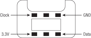
Figure 13.24 Wii nunchuck pinout
The data transmitted on these SPI pins varies based on how the manufacturer of the device (or controller) chooses to format it. In this way, the data across an I2C or SPI bus is specific to whatever you are attempting to target. Read more on how to spy on these busses in the following sections.
Finding JTAG Pinouts
Finding JTAG pinouts can be daunting. As described in great detail earlier, the pinouts for JTAG Serial Wire Debugging (SWD) depend on the manufacturer of the target device. Looking at standard JTAG headers, like those used in development kits and evaluation kits, it is clear that there can be many pin configurations. Figure 13.25 shows the most common headers.
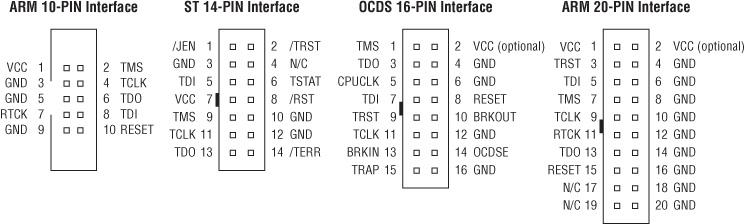
Figure 13.25 Common JTAG header pinouts
If there are so many possibilities in controlled environments like these, then what can you expect from devices in the wild?
Thankfully, as mentioned earlier, the reality is that for JTAG SWD there are only a few pins that are actually needed to perform basic debugger functionality. Again, those pins are the following:
- TDO: Test Data Out
- TDI: Test Data In
- TMS: Test Mode Select
- TCK: Test Clock
- TRST: Test Reset
In reality, even TRST is optional as it's only used to reset the target device.
When approaching a new device, figuring out which pins from a block of unlabeled pinouts is merely a guessing game. There are some heuristics reverse engineers could apply to find pins like the clock pin. A regular square wave, like those we discussed in the section “Finding UART Pinouts,” would reveal that this was TCK. However, this process can be very time consuming to perform manually, taking days, if not weeks, depending on the target. This is due to the need to try such a large number of possible combinations.
Recently, however, hacker/reverse engineer/developer Joe Grand created an open source hardware device called the JTAGulator. It allows a reverse engineer to easily iterate through all possible pinouts and thusly brute-force JTAG pinouts blindly! The schematics, bill of materials (BOM), and firmware required for creating your own device are completely open and downloadable from Joe Grand's website at www.grandideastudio.com/portfolio/jtagulator. Further, you can purchase fully assembled and operational units, such as the JTAGulator shown in Figure 13.26 from the Parallax website at www.parallax.com/product/32115.
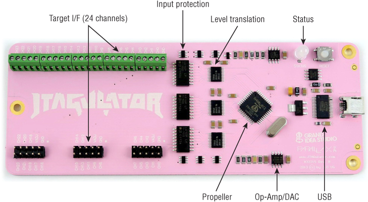
Figure 13.26 JTAGulator
With the JTAGulator, you first connect all the questionable pins to screw-down terminals or headers on the JTAGulator. Make sure that at least one pin from the target's ground plane connects the ground (GND) on the JTAGulator. The JTAGulator is USB bus powered. Connecting to the device is simple using a standard terminal program like PuTTY, GNU Screen, or Minicom.
[s7ephen@xip ˜]$ ls /dev/*serial*
/dev/cu.usbserial-A901KKFM    /dev/tty.usbserial-A901KKFM
 [s7ephen@xip ˜]$ screen /dev/tty.usbserial-A901KKFM 115200
When connected to the device, you are greeted with a friendly interactive CLI that displays the creator and firmware version:
JTAGulator 1.1
Designed by Joe Grand [[email protected]]
: :
?
:
JTAG Commands:
I   Identify JTAG pinout (IDCODE Scan)
B   Identify JTAG pinout (BYPASS Scan)
D   Get Device ID(s)
T   Test BYPASS (TDI to TDO)
UART Commands:
U   Identify UART pinout
P   UART pass through
General Commands:
V   Set target system voltage (1.2V to 3.3V)
R   Read all channels (input)
W   Write all channels (output)
H   Print available commands
:
Press the H key to display interactive help.
Joe Grand has posted videos and documentation on the web in which he uses the JTAGulator to brute force the JTAG pinouts of a Blackberry 7290 cellular phone. Still, any device with JTAG pins can be targeted with the JTAGulator. For demonstrative purposes, we chose an Android-based HTC Dream and a Luminary Micro LM3S8962 ARM Evaluation Board. To interface with the (very difficult to reach) JTAG pins of an HTC Dream we purchased a special adapter from Multi-COM, a Polish company that makes debug cables, adapters, and other low-level devices for mobile phones. After all your suspected pins are connected from the target to the JTAGulator, you select a target voltage, which is the voltage that the device uses for operating the JTAG pins. You can either guess the voltage or find it in the specifications of your target processor. The standard for most chips is to operate at 3.3 volts. The V
Current target voltage: Undefined
Enter new target voltage (1.2 - 3.3, 0 for off): 3.3
                                                 New target voltage set!
:
When that is done, it is quickest to begin with an IDCODE scan because it takes less time to perform than a BYPASS (Boundary Check) scan. IDCODE scans are written into the JTAG SWD standard as a means for a JTAG slave (in this case the target device/processor) to quickly identify itself to a JTAG master (in this case our JTAGulator).
The JTAGulator quickly iterates through the possible pin combinations initiating this rudimentary communication. If the JTAGulator gets a response, it records what pin configurations yielded a response from the device. Consequently, it is able to determine which pins provide which JTAG functions.
To perform this against an HTC Dream, initiate an IDCODE scan using the I
Enter number of channels to use (3 - 24): 19
Ensure connections are on CH19..CH0.
Possible permutations: 6840
Press spacebar to begin (any other key to abort)…
JTAGulating! Press any key to abort…
TDI: N/A
TDO: 4
TCK: 7
TMS: 5
IDCODE scan complete!
:
The JTAGulator then displays all the possible combinations of pinouts it will try and initiates brute forcing at your command. Almost instantly it gets responses, identifying which pin configurations yielded IDCODE scan responses. You can now connect these corresponding pins into your J-Link or other JTAG debugger and begin debugging the target device!
Connecting to Custom UARTs
Many cell phones, including Android devices, expose some form of UART through the use of a nonstandard cable. These cables are often called jigs. The name comes from metalworking and woodworking, where it means a custom tool crafted to help complete a task. You can find more information on jigs for Samsung devices, including the Galaxy Nexus, in the XDA-Developers forum at http://forum.xda-developers.com/showthread.php?t=1402286. More information on building a UART cable for the Nexus 4 which uses the device's headphone jack, is at http://blog.accuvantlabs.com/blog/jdryan/building-nexus-4-uart-debug-cable. Using these custom cables enables access to UART, which can also be used to achieve interactive kernel debugging as shown in Chapter 10.
Identifying Components
In previous sections there was mention of using specification sheets on target processors and devices to obtain information, but little mention was made regarding how you might go about acquiring these specifications. Virtually every IC (integrated circuit) chip generally has alphanumeric strings printed on the top surface. If you are interested, you can find many Internet resources that give excruciating detail about the format of those strings. The important thing to you as a reverse engineer or vulnerability researcher is that using a search engine enables you to quickly get information about what a chip does.
Searching for components on the Internet generally returns the manufacturer's website or the datasheets of large distributors, such as Digi-Key and Mouser Electronics. The websites of the distributors are quite useful because they generally summarize what the component is and the purpose it serves. Further, they often provide the datasheets for the products they distribute.
Getting Specifications
Although the general description of a component is useful for quickly determining its purpose on a PCB, sometimes you need a bit more information, such as the placement and location of important pins. For example, many PCBs will (for debugging purposes) connect a pin from an IC to an open hole. These open holes are called test points.
As an aside, test points are generally just that: small holes in the PCB that give an engineer test access to that line. Test points or test pads are the most common ways to expose lines. However, they are not as convenient as pin headers protruding from the board. In earlier examples, we connected to unknown pins on a PCB via these overt pin headers. Hardware hacker Travis Goodspeed's technique for interfacing with these pins is rather novel. He uses hypodermic syringes, which are extremely sharp and conductive pieces of metal (the syringe) connected to an easy to manipulate handle (the plunger). An example of this technique in action is shown in Figure 13.27.
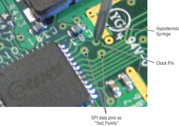
Figure 13.27 Goodspeed's syringe technique
Using this technique you can get precise access to a test pad or test point. You can clip your probes or devices to the metal of the syringe instead of cumbersomely soldering to test points that are often close together or otherwise in space-constrained positions.
Nonetheless, identifying the test points around a processor or IC can be a good first start. However, when tracing these connections back to pins on an IC, you need to know what those pins on the chip are. Pulling the specification sheets for an IC helps identify those pins.
In specification sheets, generally there are diagrams of the basic chip layout. In the event that there aren't, ICs generally have identifying notches or cut corners that identify which pin is pin 1 or pin 0. Figure 13.28 shows a few different possibilities.
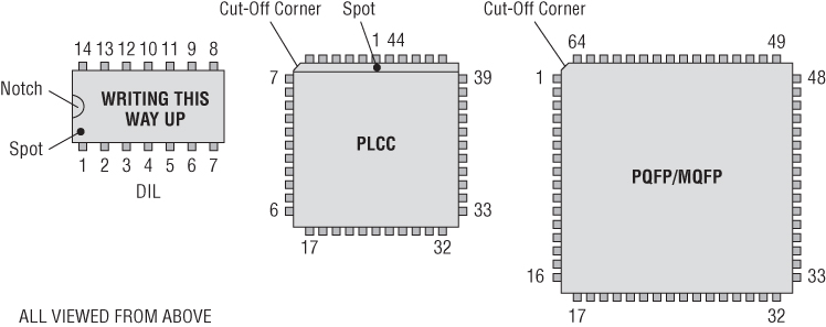
Figure 13.28 Finding pin 1
Difficulty Identifying Components
There are some cases when identifying components on a PCB can be difficult. In some cases, vendors cover the chip in epoxy or remove the silkscreen printing. In rare cases, some manufacturers—specifically CPU or microprocessor manufacturers—print “SECRET” or a project code name on an IC. Thankfully, these cases are very rare and seldom seen in consumer electronics.
Package on Package
One common obfuscation technique is something referred to in the industry as Package on Package (PoP) configurations. These are generally used by manufacturers to sandwich components together to save real-estate space on the PCB. Instead of positioning a component adjacent to a processor on the PCB and running interface lines to it, the manufacturers instead build vertically and put the component on top of the CPU. They then sell it as a package that can be purchased in different configurations by the device manufacturer. Figure 13.29 illustrates one potential PoP configuration.
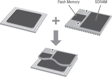
Figure 13.29 Package on Package
This practice is most commonly used (in our experience) with microprocessors and memory. Instead of putting a bank of flash memory horizontally adjacent to a CPU, some manufacturers use a PoP configuration. In this case, the only visible serial number is that of the memory atop the processor. In these cases, doing an Internet search for that serial number does not yield the specifications for what you'd expect (the microprocessor).
The solution to this can depend on the device. Sometimes the manufacturer of the visible device is the same as the manufacturer for the device underneath it. Sometimes a specification sheet for the top device yields a number of compatible devices that could be packaged with it. There is no one solution in this case, and it takes some sleuthing to find the name of the hidden device. In some cases, you can find third-party information — such as details about tear-downs performed by other technology enthusiasts — that can yield information for common consumer devices.
Intercepting, Monitoring, and Injecting Data
Intercepting data or observing the device under its normal operating conditions is a staple of vulnerability research for both software and hardware. Ultimately the goal is to observe data streams that you can either corrupt, tamper with, malform, or play back to affect some vulnerability in the target. Hardware vulnerability research is no different.
In fact, in most cases these kinds of attacks are more fruitful in embedded systems as most firmware developers or embedded developers assume that the hardware barrier to entry is too high. However, it's common that the firmware or embedded developer doesn't even conceive of the data being malformed as he often writes the software on both sides of the conversation (be it a driver or another component). Frequently no care is taken to sanity-check input values. This is often an oversight or merely a speed optimization.
This section briefly describes some of the tools that can be used to observe data on various communications lines found in embedded devices. First, it covers methods used for USB, because it is often exposed externally. Then the discussion turns to techniques for monitoring the less often exposed I2C, SPI, and UART communications.
USB
USB is perhaps the most common device interface around. It is used in virtually every mobile device and embedded device. Every Android device has an exposed USB port. Perhaps because of its ubiquity, it is also very misunderstood. The USB protocol is quite complex; so for the purposes of brevity this section only delves into some high-level parts of it.
An outstanding resource for dissecting and understanding the USB protocol is USB Complete: The Developer's Guide by Jan Axelson. Even if you don't intend to understand USB in its entirety, this publication is highly recommended if only for the first few illuminating chapters. The first few chapters succinctly introduce you to the different facets of USB, such as the transfer modes, versions, and speeds. Due to the way we often use USB as a point-to-point interface, we lose sight of the fact that USB is actually a network with a multitude of devices and hosts able to communicate along the same bus. An electronic version of the book will make searching much easier should you choose to use it as a resource later during your research.
With this book as a reference, you can comfortably begin dissecting or analyzing USB traffic. But what tools can you use to observe USB devices in the wild?
Sniffing USB
There are a number of devices available on the market that you can use as USB debuggers or protocol analyzers. Perhaps the best of them all are those made by Total Phase. Total Phase manufactures a number of wire-line protocol analyzers, including ones for SPI, CAN, I2C, and more. While we will discuss these later, Total Phase's USB analyzers are the best on the market. Total Phase makes several USB protocol analyzers at several different price points. All their devices (including the non-USB analyzers) use a common software suite called Total Phase Data Center. Each device varies in price and capabilities, with the main differences in capability being the speed of the USB bus that it can analyze. The more expensive devices can do fully passive monitoring of USB SuperSpeed 3.0 devices; the middle-tier devices can monitor USB 2.0; and the least expensive devices are only capable of monitoring USB 1.0.
At a high-level, the USB specification makes a distinction between things as either USB hosts or devices. This distinction is made within the USB controllers. USB hosts generally consist of larger devices such as desktop computers and laptops. USB devices are generally smaller devices — thumb drives, external hard-drives, or mobile phones, for example. The difference between hosts and devices becomes increasingly relevant in later sections. The Total Phase analyzers sit in-line between the USB host and USB device to passively spy on the communication between the two.
The Total Phase Data Center application controls the Total Phase analyzer hardware via a USB cable. The user interface for the Data Center application is presented in Figure 13.30.
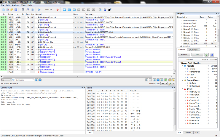
Figure 13.30 Total Phase user interface
This application is functionally equivalent to the well-known open source Wireshark network monitoring tool, but it's for USB. It enables you to record and view the protocol conversation, as well as dissect it and analyze it in a number of ways. Total Phase also exports an application programming interface (API) that enables you to interact directly with their devices or software to perform captures, receive callbacks/triggers, and passively parse or manipulate data from the bus.
In addition to the power of all this, Data Center also includes many other features, such as the ability to add comments in the data stream, online help for references to USB protocol lingo, and amazingly useful visualization tools for tracking and analyzing USB data as it flies across the bus. One such tool is Block View, which enables you to view protocol data visualized in the protocol packet hierarchy of the USB protocol. Block View is shown in Figure 13.31.
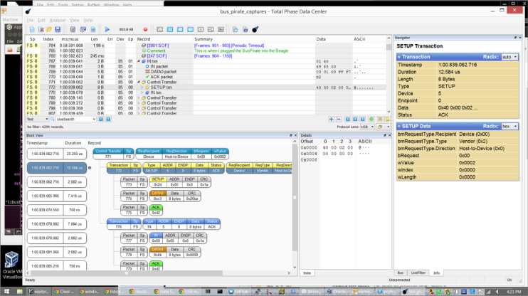
Figure 13.31 Total Phase Block View
For passively monitoring data on a USB bus, Total Phase takes the cake. It does virtually everything you could want to do with data you observe for any protocol. However, when the time comes that you need to actively interface with USB devices, the Total Phase tools are simply not designed to do that. They do not do traffic replay or packet injection of any kind.
Depending on your target, you can go about this in several ways. The main way you choose to go about actively replaying or interfacing with USB devices at a low-level USB protocol level depends on your target and desired goal. All of these differences are rooted in whether you want to interface with the target as a USB host or a USB device. There are different ways to go about both.
Interfacing with USB Devices as a USB Host
Perhaps the easiest way to go about interfacing with a target is as a USB host. If your target designates itself as a USB device (which can be observed with passive monitoring using a tool like the Total Phase) then you can use libusb
libusb/devlibusblibusblibusb
There are quite a few examples available on the Internet of people using PyUSB or high-level languages to communicate with devices such as the Xbox Kinect, human interface devices (or HIDs, such as keyboards and mice), and more. Should you choose to go that route, libusb
Interfacing with USB Hosts as a USB Device
In contrast to interfacing with USB devices, interfacing with USB hosts as a device is a much more complex issue. Because USB controllers declare themselves as either devices or hosts, you cannot easily tell the USB controller in your laptop or desktop computer to simply pretend to be a USB device. Instead, you need some form of intermediary hardware. For many years, devices that performed this function were virtually nonexistent. Then, several years ago, Travis Goodspeed unveiled an open source hardware device he called the Facedancer. The PCB layout of version 2.0 of the Facedancer appears in Figure 13.32. This device uses special firmware for the embedded MSP430 processor to accept data from a USB host and proxy it to another USB host as a device.
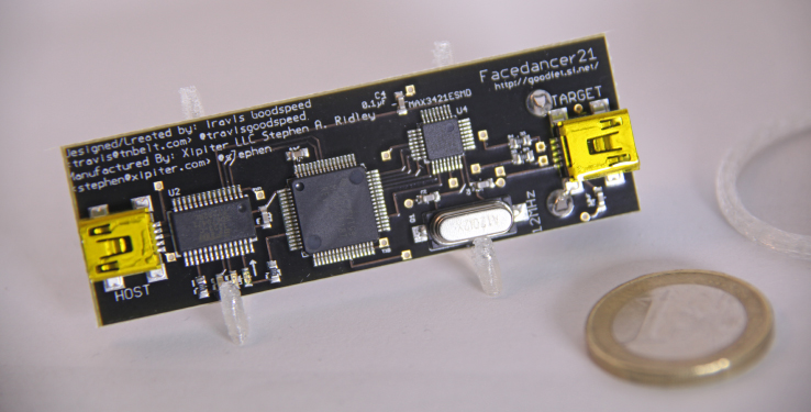
Figure 13.32 Facedancer v2.0
Unfortunately, version 2.0 of Facedancer had some simple circuit errors that were corrected by Ryan M. Speers. Travis Goodspeed has since deprecated the Facedancer20 design and with Speer's fixes released the Facedancer21.
The Facedancer device is fully open source and the code repository for the device includes Python libraries that speak directly to the hardware via USB. Developers can then use those Python libraries to write programs that speak to other USB hosts (via the Facedancer) as if they were USB devices.
The Facedancer code includes several examples out of the box. One such example is an HID (keyboard) that when plugged into a victim's computer will type messages to the victim's screen as if she were using a USB keyboard. Another example is a mass storage emulation, which allows a developer to mount (albeit slowly) a disk image (or any file) from the controlling computer onto a victim's computer as if it were a USB flash drive.
The Facedancer started off as an electronics hobbyist project. Travis Goodspeed had fabricated the PCB, but because assembly is a very expensive task to perform in bulk, it was up to the purchaser to acquire all the parts and solder it together. However, at the time of publishing, the INT3.CC website at http://int3.cc/ sells fully assembled Facedancer21 units.
There are other devices that have since released that assist with low-level USB development in the same way as the Facedancer. One such device is called SuperMUTT. It was created out of collaboration between VIALabs and Microsoft. The device is intended to work with the Microsoft USB Test Tool (MUTT, hence the name of the device). It claims to be able to simulate any device traffic on the bus, and is apparently the preferred tool of USB developers.
Whichever device you choose, it is now possible to programmatically simulate a USB device where previously it required obscure hardware tools or custom hardware development.
I2C, SPI, and UART Serial Interfaces
Earlier in the chapter, we briefly discussed I2C, SPI, and UART, describing some of the ways that they are commonly used in circuits. I2C and SPI are generally used for intra-circuit communication — that is, communication between ICs and components in a system. In contrast, UART is generally used to interface with users (interactively or as a debug interface) or larger peripherals such as modems. But how might you intercept traffic on these busses or inject data into them?
Sniffing I2C, SPI, and UART
Earlier, when detailing how to find UART pinouts, we introduced the use of a logic analyzer to record traffic on the bus. We mentioned that tools like the Saleae have software filters that can be used to intelligently guess what serial protocol is being observed. In the earlier example, a UART analyzer was used to find and decode the data output by mysterious pins exposed inside a Broadcom cable modem.
The Saleae performs analysis for I2C and SPI serial communications in much the same way. However, there are other tools that can be used to observe traffic specifically on I2C and SPI ports.
Total Phase makes a relatively low cost USB-controlled device called the Beagle I2C that can observe and analyze I2C and SPI data. The Beagle uses the Data Center application that was discussed earlier in this chapter in the “Sniffing USB” section. The Data Center interface is more suited to protocol analysis than that the interface Saleae Logic Analyzer, which simply observes square waves and guesses at protocols.
In Figure 13.33, the Total Phase Beagle was used to sniff the I2C pins of a VGA cable. Specifically, we intercepted the Extended Display Identification Data (EDID) protocol exchange that happens between a video display and a video card. In this case, the EDID data was intercepted as a monitor was plugged into a computer via a custom-made video tap, which enabled us to access all pins in a VGA cable while it was in use between a monitor and computer.
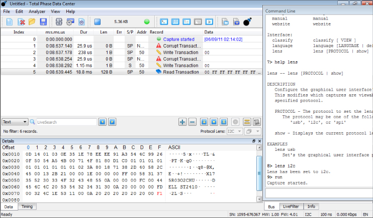
Figure 13.33 Total Phase Beagle DVI cable
Like UART, SPI and I2C can run at various speeds, so it is important that you attempt to decode at the correct baud rate. Both the Saleae and Total Phase can guess the baud rate pretty accurately using the clock pins. However, there are some small differences to note.
I2C, unlike UART, is used to network multiple components that might live on a PCB. Much like JTAG, each I2C device declares itself as either a master or a slave. Each device connected to the I2C bus (when active) changes the voltage on the overall I2C loop because it consumes the voltage causing an overall voltage drop on the line. When all devices in the I2C chain are inactive, they act as if they are disconnected from the circuit. To keep the voltage draw on the I2C lines, I2C requires a pull-up resistor on the clock and data pins to keep the voltage up even though a component in the chain is inactive. A “pull-up” resistor does exactly that; it “pulls” the voltage up to the expected levels.
As you might imagine, connecting a probe or analysis device (such as the Beagle) to an I2C bus might also change the voltage on the line. Consequently, when connecting an analysis tool to a line, you might need a pull-up resistor to pull the voltage up to the correct level. Fortunately, many I2C analysis tools take this into consideration and internally have pull-up resistors you can enable or disable with software switches. This feature exists in the Beagle analysis tools as well as the Bus Pirate, which is covered in the next section.
Talking to I2C, SPI, and UART devices
So how might you begin to interactively or programmatically speak to I2C, SPI, and UART devices? Perhaps the lowest cost method for this is to use a device called the Bus Pirate, which is shown in Figure 13.34.
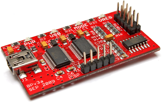
Figure 13.34 Bus Pirate v3
The Bus Pirate started off as a hobbyist device on the website Hack-A-Day (http://hackaday.com/), but quickly proved to be widely useful outside of the hobbyist community. It is extremely low cost, and you can buy it from a number of online retailers for around $30.
Much like the JTAGulator mentioned earlier, the Bus Pirate is a USB device that has a helpful CLI. You can access it using any terminal emulation program — such as PuTTY, Minicom, or GNU Screen — via a USB cable on a host computer. The following excerpt shows the help screen that can be accessed using the ?
[s7ephen@xip ˜]$ ls /dev/*serial*
/dev/cu.usbserial-A10139BG    /dev/tty.usbserial-A10139BG
 [s7ephen@xip ˜]$ screen /dev/ tty.usbserial-A10139BG 115200HiZ>
HiZ>?
General                                 Protocol interaction
---------------------------------------------------------------------------
?       This help                       (0)     List current macros
=X/|X   Converts X/reverse X            (x)     Macro x
˜       Selftest                        [       Start
#       Reset                           ]       Stop
$       Jump to bootloader              {       Start with read
&/%     Delay 1 us/ms                   }       Stop
a/A/@   AUXPIN (low/HI/READ)            "abc"   Send string
b       Set baudrate                    123
c/C     AUX assignment (aux/CS)         0x123
d/D     Measure ADC (once/CONT.)        0b110   Send value
f       Measure frequency               r       Read
g/S     Generate PWM/Servo              /       CLK hi
h       Commandhistory                         CLK lo
i       Versioninfo/statusinfo          ^       CLK tick
l/L     Bitorder (msb/LSB)              -       DAT hi
m       Change mode                     _       DAT lo
o       Set output type                 .      DAT read
p/P     Pullup resistors (off/ON)       !       Bit read
s       Script engine                   :       Repeat e.g. r:10
v       Show volts/states               .      Bits to read/write e.g. 0x55.2
w/W     PSU (off/ON)            <x>/<x= >/<0>   Usermacro x/assign x/list all
HiZ>
You can connect the Bus Pirate to the target pins of your SPI, I2C, or UART bus using a convenient bundle of probes that plug directly into the Bus Pirate, as shown in Figure 13.35.
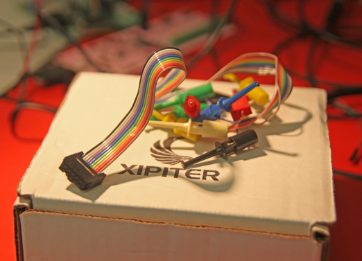
Figure 13.35 Bus Pirate probes
Unlike the JTAGulator, which guesses pinouts, the Bus Pirate probes need to be connected to the target bus in specific configurations depending on what you are targeting. You can use probe-color-coded Bus Pirate cheat sheets that are widely available on the Internet to make the Bus Pirate interface with SPI, I2C, and UART devices. For these interfaces, you need to tell the Bus Pirate some details, like baud rates (see Figure 13.36), which you can intelligently guess using tools like the Saleae discussed earlier.
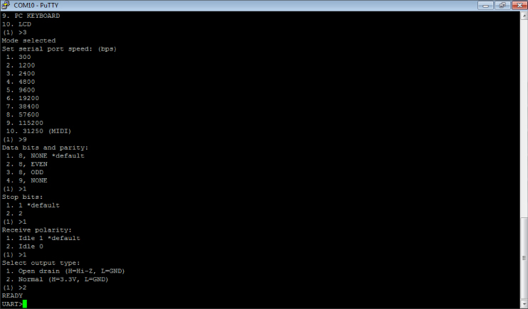
Figure 13.36 Bus Pirate baud rate setting
After it's connected, the Bus Pirate enables you to interactively or passively communicate with the target bus. Because the Bus Pirate interface is text based, it does not have an easy way to observe binary data on these busses. The Bus Pirate displays binary data by printing byte values (for example, 0x90). This is not optimal for interacting with binary data streams. In many cases, people have written their own software using libraries like PySerial to control the Bus Pirate, receive its ASCII data stream, and convert the bytes they care about back to their literal byte values.
To fill this gap, Travis Goodspeed developed the GoodFET, which acts as a Python API–controlled Bus Pirate. It is (unlike the Facedancer21) available fully assembled from a number of retailers. Using the GoodFET, you can programmatically interface with the busses you need to receive or transmit binary data outside the range of ASCII-printable characters.
Boot Loaders
After you have interactive connectivity to a device, the first thing you may encounter when the device is reset is messages from the boot loader. Many boot loaders, such as Das U-Boot or U-Boot for short, allow you a small window of time to press a key to enter an interactive boot loader menu. Figure 13.37 shows a screenshot of such a prompt in U-Boot.
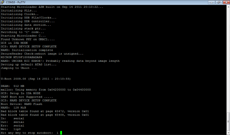
Figure 13.37 U-Boot boot message
This case alone can often lead to complete compromise of a device because the boot loaders often provide a plethora of functionality such as the following:
- Reading or writing to flash memory
- Booting from the network
- Upgrading or accepting new firmware via serial port
- Partitioning or manipulating flash file systems
Figure 13.38 shows the full extent of the commands provided by a typical U-Boot deployment.
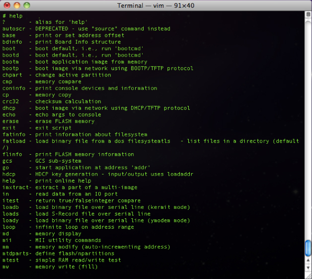
Figure 13.38 UBoot UART session
Many devices with accessible UART that make use of a boot loader like U-Boot will often let you interactively drop into a session like this. If the manufacturer did not think to disable UART, generally it also leaves U-Boot exposed.
Stealing Secrets and Firmware
Heretofore, we have discussed only methods of interfacing with and observing data on communication paths between components or devices. Perhaps using all the previously mentioned techniques you begin fuzzing and observing exceptions or crashes. Or perhaps you don't want to fuzz and simply want to import a binary image into tools like (Interactive Disassembler) IDA to reverse engineer and audit for vulnerabilities.
But how do you access data embedded in other ways?
Accessing Firmware Unobtrusively
There are many cases in which you can access and obtain firmware images from a device with fairly simple nondestructive techniques. The first method relies entirely on the kind of storage a device uses. In some rare cases, instead of a firmware image being stored to NAND or some other flash memory, it can be squirreled away (often for backup) in Electrically Erasable Programmable Read-Only Memory (EEPROM).
SPI EEPROM
Much like the SPI devices mentioned earlier in this chapter (accelerometers and temperature sensors, for example), SPI EEPROM makes use of SPI. Where other types of memory use custom interfaces and “address lines” to fetch and store data, SPI EEPROM uses a simple serial line to read and write data. The way these kinds of storage devices work is simple. An address is written to the SPI or I2C bus (for example, 0x90) and the EEPROM device responds with the data that is at that location. Figure 13.39 is a screenshot of the Total Phase Beagle observing a device reading and writing from an I2C EEPROM.
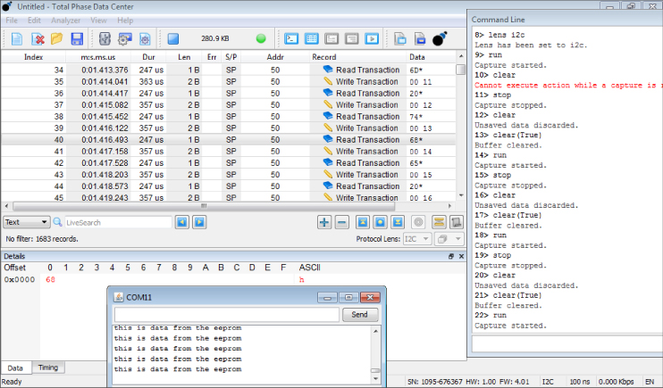
Figure 13.39 Total Phase Beagle I2C EEPROM
In the Transaction ViewWrite TransactionRead Transaction
Should you want to do more than observe a CPU make use of this kind of EEPROM, Total Phase Data Center has additional functionality for reading data directly from SPI or I2C EEPROM automatically. Using this functionality, you can reconstruct the binary data as a file on your local file system. You could also conceivably use the Bus Pirate or GoodFET to perform the same function.
MicroSD and SD Cards for Firmware Image Storage
Some devices take firmware upgrades or store firmware images on MicroSD or SD cards. In the case where those storage devices make use of a mountable file system, it is merely a matter of unplugging and mounting the device in your analysis computer. In some cases, embedded developers write the data raw, or in their own format, to the SD cards. Remembering that MicroSD and SD cards are inherently SPI, you can apply the same technique to the one described in the preceding section for reading and writing from an SPI EEPROM.
JTAG and Debuggers
You can use a JTAG debug interface or a debugger to inherently view contents of processor registers. In addition, you can often view the contents of memory. On embedded systems, specifically those executing bare metal images, this means that you can consequently extract firmware. This is another reason that gaining JTAG debugger access to a device can be extremely advantageous. Many tools, such as the Segger J-Link, use the JTAG functionality to reconstruct the firmware image on the file system of the controlling computer. Using the GDB server functionality for the J-Link, the GDB memory dump
Destructively Accessing the Firmware
There may be times where some of the previously described unobtrusive techniques are not possible. For these cases there are more obtrusive techniques.
Removing the Chip
Perhaps the most obtrusive and destructive technique for obtaining a firmware image is to physically remove the chip from the board and read it. At first glance, this may seem like a laborious and highly skilled technique. In reality, it is not.
De-soldering a surface mounted device (SMD) and reading it can be quite easy and fun. Some people use heat guns (which are essentially hot hair dryers) to simultaneously melt all solder on the connections that bind a SMD component to a PCB. This is very effective and straightforward method.
Another technique is to use a product called Chip Quik. Kits, like the one shown in Figure 13.40, come with everything needed to apply this product.
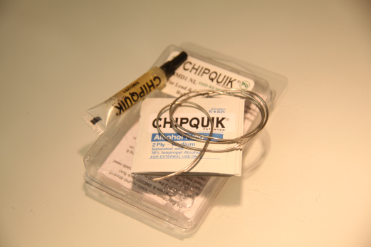
Figure 13.40 A Chip Quik kit
Chip Quik is essentially composed of a metallic alloy that has a lower melting temperature than traditional solder. Applying molten Chip Quik to solid/cooled solder transfers heat to the solder and consequently melts it. Because the Chip Quik stays hotter longer, this enables you enough time to remove or de-solder chips from PCBs. Even if you are horrible at soldering, you can effectively apply Chip Quik clumsily and have great success. There are many demonstration videos on the Internet that describe the whole process.
After the target CPU or flash chip is de-soldered from the board, then what? Fortunately, a company called Xeltek has built a family of useful devices that help with the next part: reading the chip. Xeltek offers a number of devices called Universal Flash Programmers; their top-of-the-line devices are in the SuperPro line. The SuperPro devices can essentially read and write hundreds of different kinds of flash memory and processors. One such product is the Xeltek SuperPro 5000E, which is shown in Figure 13.41.
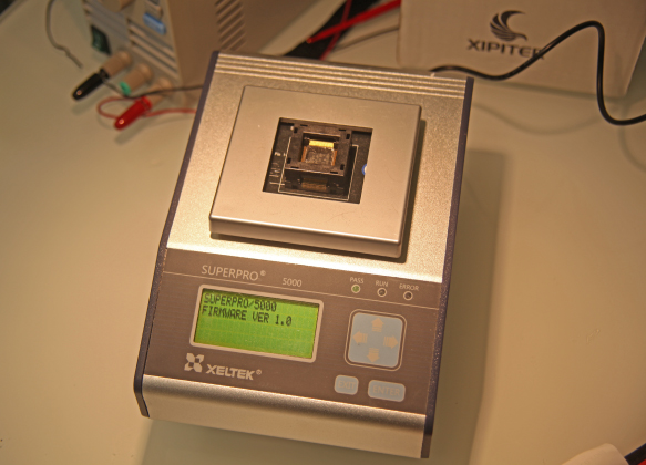
Figure 13.41 Xeltek SuperPro 5000E
In addition, Xeltek makes hundreds of adapters that fit all the possible formats and form factors that chips may take. Figure 13.42 shows some of the adapters for the SuperPro 5000E.
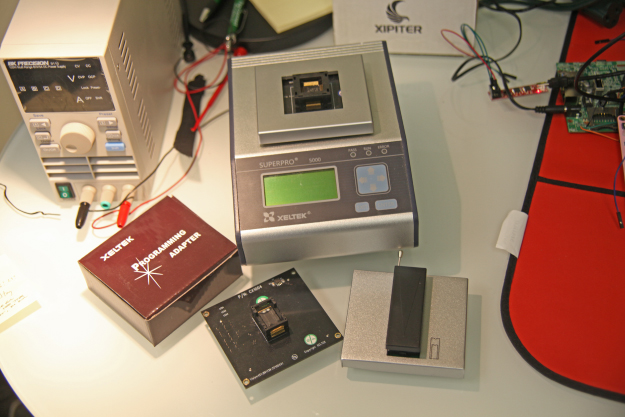
Figure 13.42 Xeltek SuperPro 5000E with adapters
The Xeltek website even has a searchable database in which you can enter a chip serial number to find out which Xeltek adapter will fit your target chip! The Xeltek device itself plugs into a computer using a USB cable and the included software is equally as simple to use. You simply start up the application, which detects the adapter type you are using and asks you if you want to read it. Click Read and a few minutes later there is a binary file on your file system of the contents of the chip! Figure 13.43 shows a screenshot of this tool in action.
Figure 13.43 Xeltek firmware read
It is literally that simple to rip the firmware out of chips. Priced at several thousand dollars, the Xeltek devices (like the advanced Total Phase USB tools) may be prohibitively expensive if you don't have a business need for them, but they provide an incredibly useful and simple function.
What Do You Do with a Dump?
So maybe you have a big binary file you've managed to extract from a device using some of the techniques mentioned previously. What next? How do you know what you are looking at? Is the binary file just the firmware or is other data intermingled?
Bare Metal Images
As mentioned earlier, microcontrollers blindly execute whatever it is they are pointed at during boot. The specifications sheet for your target tells you exactly how bootstrap works within the processor (where the entry point is, initial register states, and so on). But maybe you just want to quickly know what you are looking at. Sometimes this might require walking through the file in a hex editor to glean clues about what is in the big binary blob.
In many cases, the extracted firmware image is not just the firmware. It might also include tiny file systems like CramFS, JFFS2, or Yaffs2. In cases where you extracted data from NAND flash, these binary blobs are likely to be strictly the tiny file systems. Tools like binwalkbinwalkbinwalk
[s7ephen@xip ˜]$ binwalk libc.so
/var/folders/jb/dlpdf3ns1slblcddnxs7glsc0000gn/T/tmpzP9ukC, 734:
Warning: New continuation level 2 is more than one larger than current
level 0
DECIMAL       HEX           DESCRIPTION
----------------------------------------------------------------------
0             0x0           ELF 32-bit LSB shared object, ARM,
version 1 (SYSV)
271928        0x42638       CramFS filesystem, little endian
size 4278867 hole_support CRC 0x2f74656b, edition 1886351984,
2037674597 blocks, 1919251295 files
In this simplified example, we execute binwalklibc.so
binwalk
[s7ephen@xip ˜]$
s7s-macbook-pro:firmware_capture s7$ ls -alt Stm32_firmware.bin
-rwxrwxrwx  1 s7  staff  1048576 Mar 14  2013 Stm32_firmware.bin
[s7ephen@xip ˜]$ binwalk Stm32_firmware.bin
/var/folders/jb/dlpdf3ns1slblcddnxs7glsc0000gn/T/tmprDZue9, 734:
Warning: New continuation level 2 is more than one larger than current
level 0
DECIMAL       HEX           DESCRIPTION
----------------------------------------------------------------------
[s7ephen@xip ˜]$
In the preceding example, binwalk
Importing into IDA
If you know enough about the binary image to carve out any unnecessary bits, or if the executable binary image was obtained using other means, then importing into IDA is the next step. Importing binary images into IDA often requires some shoe-horning. Loading a binary from an embedded system into IDA is unfortunately not as straightforward as it is with ELFs, Mach-O, and Portable Executable (PE) executable images. That said, IDA does offer a lot of functionality to assist the reverse engineer with loading and parsing firmware images.
When loading a firmware image into IDA, you generally have to follow a three-step process. First, open the file with IDA and select Binary File or Dump as shown in Figure 13.44.
Figure 13.44 IDA select Binary File
Next, select the target's architecture from the dialog shown in Figure 13.45. You need to know enough about the architecture of your target processor to select it (or one close to it).
Figure 13.45 IDA select processor
Finally, you need to know enough about your target to complete the form shown in Figure 13.46. This dialog essentially informs IDA about the entry point of the binary. You can gather some of this information from the specifications sheet of your target processor.

Figure 13.46 Specifying Load Addresses in IDA Pro
At this point, if you are fortunate, IDA loads the binary. When used to reverse engineer PEs, ELFs, or Mach-O binaries you may have only noticed Fast Library Identification and Recognition Technology (FLIRT) when it has failed to help you (disassembling function entry or incorrectly identifying structures, for example). But with firmware reverse engineering, FLIRT really shines. You can access the FLIRT dialogs at any time by selecting the flower icon from the toolbar as shown in Figure 13.47.
Figure 13.47 IDA FLIRT Signatures Toolbar icon
Much like binwalk
Figure 13.48 IDA applying FLIRT signatures
This whole process is very much imperfect, but there are use cases for it on the Internet (generally for video game ROMs and such). Anticipate spending time fiddling with IDA configurations quite a bit. Even when the binary appears to be properly loaded in IDA, you can also anticipate performing quite a few additional fix-ups in the middle of the disassembly. In the case of ARM code, additional fix-ups will likely be required because IDA will likely have difficulty identifying the function entry points or the instruction mode (ARM or THUMB). You'll simply have to perform these bits manually or make use of custom IDC or IDA Python scripts to help you out.
Pitfalls
Hardware-based reverse engineering and vulnerability research can be extremely rewarding but not short of some complicating factors that can be quite frustrating to overcome. As such, here are some common pitfalls that you might encounter.
Custom Interfaces
Perhaps one of the most time-consuming and potentially annoying things to encounter on devices is custom hardware interfaces on seemingly standard pins. Generally these custom interfaces pique your interest based on their location on the PCB, such as close to the main processor. Tracing the lines from these interfaces to pins on the processor can often yield useful information. For example, if several lines are traced to pins that you know from the data sheet are responsible for USART (Universal Synchronous and Asynchronous) or JTAG then you can often deduce that these are debugging interfaces. These kinds of interfaces are often also situated close to the target processor.
However due to the unfamiliar interface, in these cases you will often need to find the mating connector for the questionable interface and break out the pins to more standard headers.
A company called SchmartBoard makes hundreds of little boards that you can use to build break-outs for strange connectors and other SMT (surface mounted) components.
Binary/Proprietary Data
Standard interfaces, such as UART, I2C, and SPI are commonly used for plain-text data such as interactive consoles, boot messages, and debug output. However, in many cases — especially in the case of non-Linux and non-Android-based systems such as those that run an RTOS — the bus uses a proprietary protocol. In some cases this is manageable, such as if the proprietary protocol is entirely ASCII based. With an entirely ASCII-based protocol you have immediate confirmation that you have things properly configured. The fact that you can see text is a good sign. You're often also able to quickly identify patterns such as recurring characters that act as delimiters for the protocol, or a certain uniformity in formatting (e.g., sequences of floating point numbers).
However, you may encounter cases where the data on the bus is entirely binary. In these cases it can be difficult to even be sure that you have correctly interfaced with the device. Did you get the wrong baud rate and data encoding? In these circumstances sometimes a combination of other techniques, such as directly accessing the firmware, can be used to help figure out what is going on.
If you are observing the mystery data on a bus between components, sometimes spying on it (using previously described techniques) and writing some simple protocol replication code to replay it will help; you might even find bugs along the way.
Blown Debug Interfaces
There are many JTAG defenses, but perhaps the most common is referred to as a JTAG fuse. These fuses can be physical (physically disconnect the JTAG lines internal to the processor) or software based. Defeating either requires advanced techniques that are outside the scope of this text. However, defeating them is possible (specifically for software fuses). Ralph Phillip Weinmann briefly discusses these techniques to re-enable JTAG debugging in the baseband processor of his HTC Dream in his USENIX paper “Baseband Attacks: Remote Exploitation of Memory Corruptions in Cellular Protocol Stacks.” Kurt Rosenfeld and Ramesh Karri have written another in-depth paper on JTAG defenses entitled “JTAG: Attacks and Defenses,” although this paper focuses more on the general theory of attacks and a proposed defense. Additionally, you can find resources on defeating the blown software fuses for specific devices on some online developer forums.
Chip Passwords
Some microcontroller manufacturers do not allow the device to be flashed unless a user-definable password is used. These passwords are a string of bytes that are sent to the bootstrap loader in the chip. This prevents flashing, but some microcontroller vendors only enable some debug functionality if a “physical” password is supplied to the chip.
Boot Loader Passwords, Hotkeys, and Silent Terminals
Some boot loaders, such as U-Boot, offer some security options to embedded developers. U-Boot has some security features that enable a developer to hide the U-Boot output or require a special hotkey, password, or special byte sequence over UART before entering an interactive U-Boot session. These cases tend to be rare as security conscious manufacturers would likely hide the UART interface as well, but they are not unheard of. Generally the firmware and hardware designers are working separately within a company or possibly even subcontracted out. In these cases, some more advanced techniques outside the scope of this text may be required to subvert these protections.
In some cases, boot messages from the boot loader, and even the operating system, may be observable, but then the line goes silent or begins spewing garbage. Sometimes, you are lucky, and the problem is merely a matter of the baud rate changing. In other cases, there are custom debug interfaces that you should attach, or you might need a driver that uses binary data to transmit debug information to a custom piece of software monitoring the UART interface of a device.
Customized Boot Sequences
There are times you may rejoice at finding and successfully interfacing with UART (or some debugging output interface). You will watch it load the boot loader and boot into the kernel. You'll watch drivers initialize and perhaps even rub your hands together in devilish anticipation for a login prompt—but it doesn't come. Why?
When this happens, generally the distribution of Linux or Android has been customized to not execute the login
In cases like this, you'll miss the familiar login prompt but you can employ other techniques to subvert the device. Perhaps breaking into the boot loader will give you access to the firmware image, or perhaps physically accessing the flash storage will provide a copy of the file system image to investigate further. These are simply some things you may try, but this might require some further investigation if simple attempts like this are unsuccessful.
Unexposed Address Lines
Previously in this chapter we mentioned that manufacturers will sometimes sandwich components like NAND flash on top of a microcontroller to save space on a PCB in a configuration known as PoP. Recall that such configurations can make it difficult to identify the serial/part number for a microcontroller. There is another pitfall to these kinds of PoP configurations.
In the case where a flash chip is mounted on a microcontroller in a POP configuration, one drawback is that the pins of the flash chip are not exposed. In fact, there are no pins. Therefore, in these cases, you cannot easily employ de-soldering techniques to remove the flash and read its contents. Therefore, the only way (barring some advanced and tedious chip-separation techniques) to access the contents of flash is to access it through the microcontroller. If the microcontroller does not have debugging capabilities disabled then this is possible. However, if, for example, the JTAG fuses have been blown, it might not be possible to easily access that data.
Anti-Reversing Epoxy
There may be some targets that you dismantle only to find that the PCB has been coated in a glossy or matte black or blue material. Sometimes this is done by manufacturers to protect the components from weather or condensation. But in most cases it is to prevent someone from easily connecting to components with probes or to prevent de-soldering components to read data from them. Some of these are simple to defeat with a razor or the combination of a razor and the focused heat of a heat gun.
Other, more expensive epoxies are mixed with a silicon-based compound. This is to thwart people from using chemical compounds to dissolve the epoxy. The reason for the silicon-based additives is that any chemical solvent that can dissolve the additive will likely also dissolve and destroy the silicon in the PCB and the component it is meant to protect, thus completely destroying the device.
Image Encryption, Obfuscation, and Anti-Debugging
We have not encountered many embedded consumer devices that use these techniques. Reverse engineers familiar with PC and mobile malware might immediately think of the encryption and obfuscation techniques such as those used in malicious software for desktop computers (dead code preceded by jumps, runtime deobfuscation, and so on). Although there are probably a number of clever and custom ways to do this within the constraints of the components of a device, they don't seem to be too common in embedded devices because of the constraints of space and computing power of a device.
For example, an encrypted bare-metal executable that decrypted itself on the fly might seem like an immediate solution. However, on an embedded system with limited RAM there may not be enough room for the full image to load. Additionally, flash memory decays with each write, so most embedded developers avoid writing to flash during execution. If an executable image is unable to perform unpacking in RAM, it would have to modify itself in flash. Doing this on every boot of the device would not only be slow, but it would wear the storage media more quickly.
Summary
This chapter is designed to bring even the most uninitiated reader up to speed on successfully leveraging physical access to attack embedded hardware such as Android devices. It covered several different types of interfaces that are commonly exposed in embedded devices, including UART, JTAG, I2C, SPI, USB, and SD cards. It explained the how and why of identifying and communicating with these interfaces. Utilizing these interfaces, researchers are able to achieve a deeper understanding of the target device.
A popular goal of physical attacks against hardware is to discover, design, and implement further attacks that do not require physical access. Using a host of commercially and freely available tools, this chapter explained how accessing these interfaces can provide access to the device's firmware. Reverse engineering the firmware provides deep insight into how the device works and may even reveal some critical vulnerabilities.
Finally, we presented potential pitfalls that you might encounter when attempting to apply these tools and techniques in practice. Whenever possible, we recommended ways to conquer these challenges and achieve success despite them.