
Chapter 4
Internal Antenna
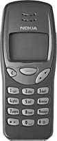
The internal antenna emerged around the end of the twentieth century and gained its popularity in merely a few years. Nokia was the first mainstream cell phone company who successfully marketed phones with internal antennas. As shown in Figure 4.1, the Nokia 3210, which came onto the market in 1999, was a huge hit and more than 300 million of them were eventually sold around the world. “Candy-bar phones,” a nickname for those phones with internal antennas strongly resonates with the European fashion taste, which appreciates minimalism and sleek curves. With that momentum, Nokia successfully eroded Motorola's market share in Europe.
Figure 4.1 Nokia 3210 Reproduced with permission from Nokia, Inc.
After that, there were a few years of de facto draw between Nokia and Motorola, who shared the first and second places on the global chart of cell phone sales. Nokia claimed that it sold the most phones and Motorola insisted that its revenue of cell phones was the highest. Both claims were correct, because Motorola was still holding onto the high-end market. What happened next was quite theatrical. Nokia wanted to use only candy-bar phones to conquer the US market but kept failing. US customers didn't want to give up their love of flip phones, which had been invented by Motorola. Nokia did not want to develop flip phones and hoped, through advertising and customer education, that Americans' attitude toward candy-bar phones could be converted in a relatively short period. Sadly, history demonstrates again how strong the persistence of people's habits is.
Nokia's love of internal antenna is not really emotional, it is because there are some technical and financial merits inherent in internal antennas. A candy-bar phone with an internal antenna has no moving parts and only one PCB circuit. A handful of screws can securely assemble all the core parts. The front and back cover, which are made of ABS plastic, are snapped onto the core without any screws. When a candy-bar phone is accidentally dropped on the ground, the covers take most of the force. Because there is no screw attached to the cover, there is no extreme stress point. When the force is too strong to bear, the snap feature just breaks loose and absorbs all energy in the process. After the drop, a candy-bar phone might fall apart, however, nothing is really broken; one can put it all back together and the phone is ready to work again. The robustness of a candy-bar phone is one of critical factors that made Nokia so successful in the markets of the developing countries. Due to the cut-throat competition, the margin of low-tier phones is razor thin, and an increase of field failure rate (FFR) by a small percentage might totally wipe out the profits.
Unlike flip phones, candy-bar phones do not have features such as flip, hinge, board-to-board connector, and so on, the shorter build of material (BOM) of candy-bar phones also means less manufacturing cost. Combining the cost-saving on the stages of both manufacturing and customer service, Nokia can sell a low-tier phone at a price which is lower than Motorola's cost and still make decent money. For Nokia, moving into the field of flip phones with external antennas meant fighting a war in its enemy's territory while losing most of its competitive advantage. Nokia's own wishful thinking was that it could corner Motorola in the US market with candy-bar phones with internal antennas combined with a price war, but apparently this didn't work.
On the other hand, Motorola did not want to fight in the field of candy-bar phones either. The reason for that is because of Nokia's fearful logistic capability and its sophisticated global sourcing system. For most components used in Nokia, there is more than one vendor in the supplier pool. By doing this, Nokia can hammer vendors and demand a lower price and mitigate the possible part shortage due to any single vendor's failure. In the meantime, the possible vendor of any component in the supplier pool is limited to a handful. There is a strict process in place to qualify a potential vendor, only heavyweight players in the according discipline have the possibility of being qualified. The strict screening process ensures the quality of parts used in phones, thus assuring the reliability in phone manufacturing. All these issues might sound quite simple, but in fact it is quite a challenge to implement them successfully.
Finally, both sides moved into their counterpart's territory. It was a fierce fight, which eventually expanded to new fields with the emergence of new form of factors, such as slide phones and swivel phones. It now all seems a distant history. When this book was written, in 2009, Nokia claimed more than 40% of the global phone market and Motorola's market share is wandering in the territory of single digit. With the blow of the current economic crisis, which is the worst since the 1930s, Motorola's fate does not look bright. However, it will be very sad day if we lose Motorola. After all, it was Motorola who invented the personal wireless communication in the first place. Who knows, a miracle might happen, just as it happened to Apple. In 1997, everything seemed against Apple, the inventor of the personal computer, and bankruptcy seemed its only fate. Then suddenly, with the return of the expelled founder Steve Jobs, everything turned around. Today, Apple is not only thriving in its traditional computer business; it has also become a significant player in the phone business. The iPhone, which Apple released in 2007 and sold more than 10 million in the first year, happens to adopt an internal antenna, which can trace its roots all the way back to the internal antenna invented a decade ago. As for Motorola, best wishes for the future.
Although to a customer, all internal antennas might have the same appearance, that is, no visible evidence of an antenna's existence, there is more than one kind of internal antennas if we categorize them from a technical point of view. We are going to discuss some of them in this chapter. The aim of this book is to introduce the world of antenna designing. With the knowledge shared in the book, one should be able to design an antenna for most applications. In some tightly constrained applications, such as designing a multi-band antenna in a tiny volume, the antennas introduced here may not be enough to fulfill the requirements. In those circumstances, a book by Professor Wong [1], Planar Antennas for Wireless Communications, provides more advanced techniques to meet such challenges.
Let's start with the inverted-F antenna (IFA). We know that a monopole antenna works pretty well for mobile applications. However, the size of a monopole is too big to be adopted in most state-of-the-art phones. Naturally, L-shaped antennas as shown in Figure 4.2 were proposed as a measure to decrease the total height of an antenna.
Figure 4.2 L-shaped antenna

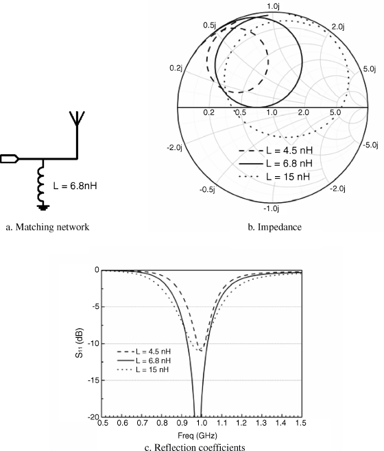
While keeping the total antenna's length, say, 70 mm, the antenna whip can be bent into an L shape in different positions, thus providing a different separation, G, from the ground plane. The dimension G is a critical parameter which decides the antenna's impedance. Shown in Figure 4.3 are simulated results of a straight whip antenna and two L-shaped antennas. When the horizontal arm approaches the ground plane, the real part of the antenna's impedance becomes smaller. That means the impedance locus sweeps a larger circle on the Smith Chart. As the impedance of a straight whip is around 100 Ω, when the whip is bent and approaching the ground, the matching of the antenna is actually improved at first. In this example, the antenna with the G equaling 14 mm is the best matched one of all three. However, if the separation between whip and ground is less than 14 mm, the matching starts to degrade.
Figure 4.3 Impact of separation G on an L-shaped antenna

Using the matching techniques discussed in Chapter 1, good matching can be easily achieved. Either a shunt inductor or a shunt capacitor can be used to match the antenna. Shown in Figure 4.4 are simulated results. A lumped inductor is used to match the antenna with G = 6 mm. The dashed line, the solid line, and dotted line correspond to three different matching values. For a shunt inductor, a smaller value has more impact on the port impedance. A 6.8 nH inductor provides the best matching.
Figure 4.4 Using a shunt inductor to match the antenna with G = 6 mm
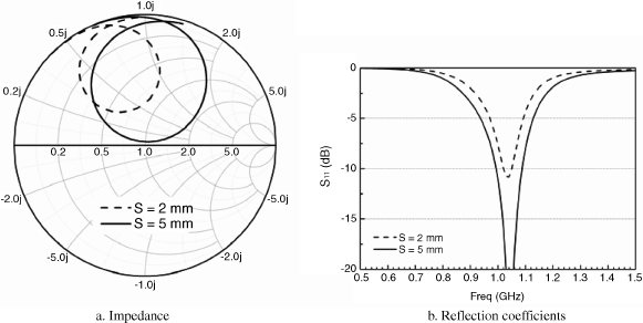
By replacing the lumped inductor with a grounding metal strip, what we get is an inverted-F antenna (IFA) as shown in Figure 4.5. The shape of the antenna element is like the letter “F” on its side, that is why it is called inverted F. Shown in Figure 4.6 are the results of two IFA antennas. For the sake of consistency, the total whip length of both antennas is kept to 70 mm if measured from the feeding point to the end of the whip. The separations between the feeding and grounding strips are chosen to be 2 mm and 5 mm respectively. Comparing Figures 4.4 and 4.6, it is clear that the grounding strip indeed functions as a shunt inductor. As the inductance of the grounding strip is decided by its total length, when the separation between the feeding and grounding strips becomes shorter, the distributed inductance become smaller, thus the grounding strip has more impact.
Figure 4.5 IFA antenna

Figure 4.6 Impact of separation S on an IFA antenna
As a rule of thumb, whenever the separation between the arm of an IFA antenna and ground gets smaller, the grounding strip must be placed closer to the feeding strip to compensate for the impedance change.
In practice, designing a single band IFA antenna is quite easy. The following are some design steps:
- Start with a strip a little longer than a quarter of wavelength. A 4 mm gap between grounding and feeding strips can be used as the starting point.
- Tune the antenna length to get a resonance, which is slightly lower than the target frequency.
- Check the impedance on the Smith Chart. The impedance must look similar to one of the three curves shown in Figure 4.4. If it resembles the dashed line, increase the gap S. If it resembles the dotted line, decrease S. The solid line is the preferred option.
- Fine tune the antenna length again until the correct resonant frequency is obtained.
Looking at Figures 4.4 and 4.6 more closely, the difference between resonant frequencies can be observed. When the antenna lengths are identical, an L-shaped antenna can work at a lower frequency. To qualitatively explain this, a simplified equivalent circuit of an IFA antenna is given in Figure 4.7. Unlike an L-shaped antenna, whose resonant frequency is decided by its whole whip, only a part of IFA antenna, which is marked by the dark color in Figure 4.7, is the active element. The effect of grounding and feeding strips can be approximated by a shunt inductor and a series inductor respectively. Of course, this is only a coarse simplification, when the distance between feeding and grounding strip become too short, the distributed shunt capacitance between two strips can also play a role in the antenna performance.
Figure 4.7 Simplified equivalent circuit of an IFA antenna

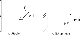
As we know that E-fields excited by a whip antenna are always parallel to the whip itself as shown in Figure 4.8 a, one might assume that the E-field generated by an IFA antenna should rotate 90 degrees, as the whip is rotated 90 degrees. In fact, the rotation of an IFA's whip has little impact on the polarization of radiation pattern. Similar to monopole antennas, an IFA cannot work by itself. It must be installed on a ground and it is the ground that decides the E-field polarization. As shown in Figure 4.8 b, when the ground is vertically placed, the E-field is also vertically polarized.
Figure 4.8 E-field excited by antennas
Shown in Figure 4.9 are simulated 3D radiation patterns of an IFA. The antenna is the same one simulated in Figure 4.6 with S = 5 mm. Shown in Figure 4.9 a is the 3D pattern of Eθ, which is the vertical polarization part of total E field. Figure 4.9 b is the Eϕ, the horizontal part of the total E-field. The amplitude unit used in both plots is dB. The scale they used is also the same. It is clear that the vertical E field is the dominant radiation component. The peak gain of the vertical E-field is 3.4 dBi. That of the horizontal E-field is only −5.8 dB. At a low frequency, such as 1.05 GHz, the radiation pattern of the ground is similar to a dipole, which is donut-shaped and approximately omni-directional in the azimuth plane. At a higher frequency, because the ground is much larger than one wavelength, the radiation pattern will split. This behavior is similar to that of a monopole antenna. Detailed studies of the ground effect can be found in Section 3.5 and published papers [2–5].
Figure 4.9 3D radiation patterns, IFA antenna, S = 5 mm, 1.05 GHz

An IFA antenna does not provide a lot of design freedom, so it is mostly used in single-band applications, such as GPS, BT, or WiFi. Although an IFA antenna is similar to an L antenna with a shunt matching inductor, there is a minor difference. Because the active length of an L antenna starts from the feeding point, it can be designed to be smaller than an IFA antenna. An L antenna also requires a smaller area on the PCB, because it only needs one contact pad. The drawback of an L antenna is that the lumped matching inductor it requires has some inherent losses, thus the efficiency of an L antenna is normally a few tenths of dB lower than an IFA antenna's. If there is enough board area for two pads, one for grounding and one for feeding, an IFA antenna is a better choice, as it provides better efficiency and also saves a matching component, which costs a few pennies.
4.2 Planar Inverted-F Antenna (PIFA)
4.2.1 Single Band PIFA
Shown in Figure 4.10 is a planar inverted-F antenna (PIFA). PIFA antennas can be thought of as a mutation of IFA antennas. Both IFA and PIFA antennas have a ground strip and a feeding strip. By replacing the radiating strip of an IFA antenna with a patch, we get a PIFA antenna. In most cases, the patch of a PIFA antenna is above the ground plane.
Figure 4.10 PIFA antenna

In all the following samples in this section, the width of both feeding and grounding strip is 1 mm; the dimension of PCB, which is used as the ground, is 50 mm∗120 mm. If the PCB size is changed, the antenna response will change accordingly. The ground's impact on a PIFA antenna is the same as that on an external antenna. Refer to Section 3.4 for further details.
In Figure 4.10, the dimension H is the distance between a patch and a ground. The S is the edge-to-edge distance between feeding and grounding strips. Similar to IFA antennas, the matching of antennas can be tuned by adjusting S.
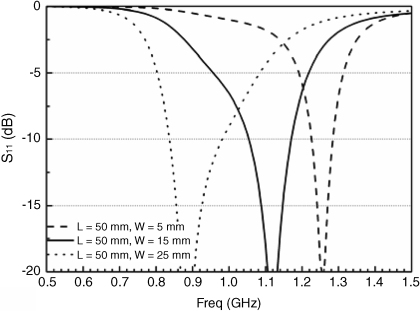
Let's start with single-band PIFA antennas. Shown in Figure 4.11 are simulated results of three PIFA antennas. The dimension L of all three antennas is 50 mm, which is the same as the PCB width. The dimension W of three antennas is 5 mm, 15 mm, and 25 mm respectively. To best match individual antennas, the dimension S, the distance between feeding and ground strips, is tuned case by case. The optimal S for 5 mm, 15 mm, and 25 mm patches are 1.5 mm, 4 mm, and 4 mm respectively. When the W is 5 mm, the antenna is more like an IFA than a PIFA. With the increase in W, the resonant frequency of a PIFA antenna decreases. This phenomenon gives us a hint that, unlike an IFA antenna, the resonant frequency of a PIFA antenna is not solely decided by the patch's length.
Figure 4.11 Three PIFA antennas with different widths H = 7 mm
For a PIFA antenna, the resonant frequency is proportional to the summary of its length and width. As shown in Figure 4.12, a PIFA's width plus its length is roughly a quarter of a wavelength at its resonant frequency.
Figure 4.12 Estimating the resonant frequency of a PIFA

When discussing a single band PIFA antenna, most books prefer to give a current distribution which shows two clear current flows. Both of them start from the upper-left corner and end at the bottom-right corner. One of them passes the bottom-left corner and the other one passes the opposite top-right corner. That is a quite intuitive but coarse simplification. The real current distribution is a little more complex than that. In many cases it is difficult to see a clear current pattern when you simulate a PIFA antenna.
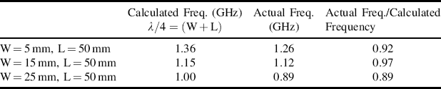
Shown in Table 4.1 is a comparison between three antennas. The second column in Table 4.1 is the calculated resonant frequencies based on the assumption that W + L equals to a quarter of wavelength. The third column is the actual frequency. The fourth column is the ratio between the calculated frequencies and the actual ones. The actual resonant frequency of a patch is normally lower than the theoretical one. That is due to the loading effect of the edge capacitance between patch and ground.
Table 4.1 Accuracy of simplified frequency calculation formula
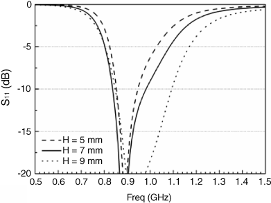
The critical parameter, which controls the bandwidth of a PIFA antenna, is H, the distance between a patch and a ground. Shown in Figure 4.13 are the reflection coefficients of three antennas with different heights. All patches have the same L and W, which are 50 mm and 25 mm respectively. The H of three patches is 5 mm, 7 mm, and 9 mm respectively. All three antennas are individually tuned, their S are 3 mm, 4 mm, and 7 mm accordingly. By increasing the H from 5 mm to 9 mm, an antenna's −10-dB bandwidth is almost tripled.
Figure 4.13 PIFA antenna's bandwidth vs. height. L = 50 mm, W = 25 mm
As a summary, there are three design guidelines for single band PIFA:
- The dimension H is the most critical parameter which decides an antenna's overall performance. However, because H is directly related to a device's thickness, it is a tough task to bargain about it with industry design engineers or mechanical engineers. If there is only a 5 mm height clearance and a quad-band GSM antenna is required, then PIFA is not an appropriate candidate. A folded monopole antenna, discussed in Section 4.3, is a better choice.
- By adjusting the total length W + L, the antenna's working frequency can be tuned. In practice, the L should be similar to the PCB's width that results in wider bandwidth.
- The dimension S is the tuning parameter which optimizes an antenna's matching. One can either use a wider strip with a larger S or a narrower strip with a smaller S to achieve the same matching. A larger S is better for manufacturing, because a fixed process tolerance causes less electrical variance in the antenna. From a mechanical point of view, a narrower strip is better for spring finger type of designs, because it is more flexible and it is easier to achieve the required spring force.
4.2.2 Multi-Band PIFA Antenna with Slits
If you have already discovered PIFA antennas, then you might find that the following explanation is somewhat different from other books. All versions of PIFA explanations are partially correct, including the following version. As a PIFA antenna is a distributed radiating system, too many parameters play a role in deciding the antenna's characteristic. To explain such a complex matter, one has to substantially simplify it and that is the reason for the different explanations.
There are several ways to design a multi-band PIFA antenna. The most popular way is to cut slits on the patch, as shown in Figure 4.14. Similar to a single band PIFA antenna, a dual-band PIFA antenna also has a grounding strip and a feeding strip. Two critical dimensions, D and C, are used here to describe the slit. The dimension D is the distance between the patch's corner and the opening of the slit. The dimension C is the slit's length. The dimension P is the distance between the horizontal part of slit and the edge of patch. The P is not really a critical dimension, however, it decides the shape of the slit.
Figure 4.14 Dual-band PIFA antenna

Shown in Figure 4.15 are the decisive paths of different bands. Figure 4.15 only serves the purpose of predicting the trends of frequency shifting when different dimensions are adjusted. One should not try to use the illustrated critical path shown in Figure 4.15 as a way of calculating a patch's resonant frequency. In reality, trying to predict a patch's resonant frequency with a calculator is not really an efficient design approach. There are always so many unknown parameters, such as the permittivity of both the antenna support and the phone cover, the electrical property of nearby objects, and so on. Usually, all these unknowns can make the theoretical calculation far removed from the correct answer. A better approach is to memorize the effect of each parameter first, then make a PIFA with a piece of copper tape, install it on a mock-up phone, cut a slit on the PIFA, and tune it by trial and error.
Figure 4.15 Decisive paths of different bands

The impacts of the two critical dimensions are listed below:
- The distance D can affect the resonant frequency of both the lower and the higher bands. It always shifts two bands in the opposite directions. For example, if we decrease D, the critical path of the lower band will be shorter, thus increasing its resonant frequency. In the meantime, the critical path of the higher band is increased, thus inducing a lower resonant frequency.
- The slit's length C only influences the higher band. The slit is about half the total critical path of the higher band. Increase C can lower the high band.
Of course, in the real world, the effect of any dimension change cannot be exclusively constrained in a single band. In fact, it is safer to claim that it has more impact on some bands than others. To help understand the design rules, the following design examples are provided. In all the following examples, the area of patch is 50 mm∗25 mm; the area of ground is 120 mm∗50 mm. H, which is the distance between ground and patch as shown in Figure 4.10, is 7 mm. The impact of D is illustrated in Figure 4.16. By adjusting D, both low and high resonances frequency can be tuned simultaneously and in opposite directions.
Figure 4.16 Impact of dimension D. 50 mm∗25 mm Patch, P = 15 mm, C = 40 mm

Illustrated in Figure 4.17 are the impacts of slot length C. With the increase of a slot's length, the resonant frequency of higher band decreases. It can be seen that the resonant frequency at the lower band still drifts a little bit. For all three cases shown in Figure 4.17, the dimension P is fixed, the modification of C is realized by only increasing or decreasing the length of the horizontal portion of the slit.
Figure 4.17 Impact of dimension C. 50 mm∗25 mm Patch, P = 15 mm, D = 10 mm

Shown in Figure 4.18 are the results when the dimension P is changed while keeping the slit length C fixed. Although not significantly, the dimension P also has some impact on the higher band. It can be used in some circumstance as a means to provide the “extra mile” for tuning.
Figure 4.18 Impact of dimension P. 50 mm∗25 mm Patch, C = 35 mm, D = 10 mm
Shown in Figure 4.19 are the radiation patterns of a PIFA antenna. At the low band, which is 0.78 GHz in this case, the radiation pattern is similar to a dipole's. The radiation is mostly generated by the vertical current along the edge of the ground plane. The vertical polarized field Eθ is the dominant field component. At the higher band, which is 1.75 GHz, the amplitudes of Eθ and Eϕ are in the same order of magnitude. Shown in Figure 4.19 e is the radiation pattern of the total E field at 1.75 GHz. It confirms again that it is the ground plane, instead of the antenna element itself, which definitively decides the radiation patterns.
Figure 4.19 Radiation patterns of PIFA antenna, P = 15 mm, D = 15 mm, C = 40 mm

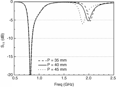
When designing any kind of antenna, antenna engineers may find themselves in a situation where one band has more than enough bandwidth but the other band cannot meet the specification. Knowing how to exchange bandwidth between bands is an essential technique. For a PIFA antenna, cutting the slit shape differently can have some effect on the bandwidth ratio between bands. The other way to change the ratio is by adjusting the slit's width. Shown in Figure 4.20 are the simulated results of three PIFA antennas with the same dimensions but different slit widths. With the decrease in the slit's width, the bandwidth increases at the lower band and decreases at the higher band.
Figure 4.20 Bandwidth trade-off between low and high bands

If an antenna still cannot meet the specification after the performance of both bands have been balanced, the only way out is to attempt to increase the patch's height, which is the dimension H shown in Figure 4.10 a. This definitely is an uphill battle.
So far, we have shown how to adjust both bands simultaneously or modify the high band independently. By combining both methods, we can tune the resonances freely in a quite wide range. Now let's discuss some matching techniques. The easiest way to match an antenna is to design a matching circuit. However, a matching circuit always has some inherent loss. For a patch antenna, some of the dimensions can be modified, so we should always try to achieve a good match by tweaking the patch itself first. By comparing Figures 4.16 and 4.17, we can see that there are different ways to cut the slit to achieve two required resonant frequencies, and their matching conditions are also different.
Besides the patch itself, another useful tuning mechanism is the feeding and grounding structure. Shown in Figure 4.21 is the equivalent circuit of feeding and grounding strips. The grounding strip is equivalent to a shunt inductor, so it has more impact on the lower band. The feeding strip is equivalent to a series inductor, and it can be used to tune the high band. To increase the inductance of grounding strip, the following methods can be used:
- Increase the length of grounding strip by bending the strip.
- Decrease the width of grounding strip, t2.
- Increase the distance between feeding strip and grounding strip, S.
Similarly, the inductance of feeding strip can also be increased by increasing the length or decreasing the width of the strip. Shown in Figure 4.22 are two other ways of matching. Figure 4.22 a shows how to use the slit to increase the shunt inductance. Figure 4.22 b shows how to add some distributed shunt capacitance. Another effect of the stub shown in Figure 4.22 b is to increase the total current length, thus decreasing the overall resonant frequency. If you have a brainstorming session on this topic, lots of matching structures can be invented. Where should we stop and hand over the remaining tasks to lumped matching element? There is no right or wrong answer to this question. Normally it is a purely personal choice. Some engineers prefer a self-matched design without requiring any lumped components. Many of those engineers treat antenna design as an art. Some engineers like to reuse previous designs and want to push dimension changes to the minimum. For them, a matching circuit is the favorite choice.
Figure 4.21 Equivalent circuit of feeding and grounding strips

Figure 4.22 Other ways of matching

Putting the personal preference aside, there are some objective criteria that can be used to evaluate any antenna design. How sensitive is a design to manufacturing tolerance? What kind of manufacturing process can it use? Is a design easy to be tuned when frequency drifts? Does frequency tuning require expensive and time-consuming tooling modifications? What is the efficiency of an antenna?
It is not difficult to imagine that the weight of each criterion varies from project to project. For a low-end phone, cost might be the first consideration. For a high-end phone, it is most likely that all physical constraints have been pushed to the limit, the only goal for an antenna engineer is to meet the specification at any cost. The duration of a project is also an important factor when selecting different approaches. In fact, most issues mentioned here are not academic at all, they are purely practical matters. Section 4.2.5 is dedicated to this topic.
Referring to Figure 4.15, if the patch size gets smaller, to maintain the resonant frequency at the lower band, the opening of the slit needs to be moved closer to the feeding point, and the slit must be routed through the other direction. Shown in Figure 4.23 is an example of such a small PIFA. The rules for tuning the small PIFA antenna shown in Figure 4.23 are pretty much the same as that shown in Figure 4.15. The critical dimensions are the slit's length and the opening position of a slit. The length of the slit has more impact on the higher band, while the slit's open position affects both bands.
Figure 4.23 A small PIFA
Shown in Figure 4.24 are the simulated results of a small PIFA antenna when the slot length varies. By decreasing or increasing the slot length by 2 mm, the resonant frequency at a higher band is shifted up or down by around 35 MHz respectively. Meanwhile, the lower band response is relatively immune to those changes.
Figure 4.24 A small PIFA: slot length variations

So far we have discussed how to design and tune a PIFA antenna. The topic of current modes on a patch has deliberately been avoided in order to minimize confusion in the first stage of learning. Although the current distribution on a patch can provide a very useful insight on how different patches work, it frequently makes a new engineer confused about how to tune a PIFA antenna. Of course, if we want to make some innovation in the field of antennas, current modes is a topic we must discuss.
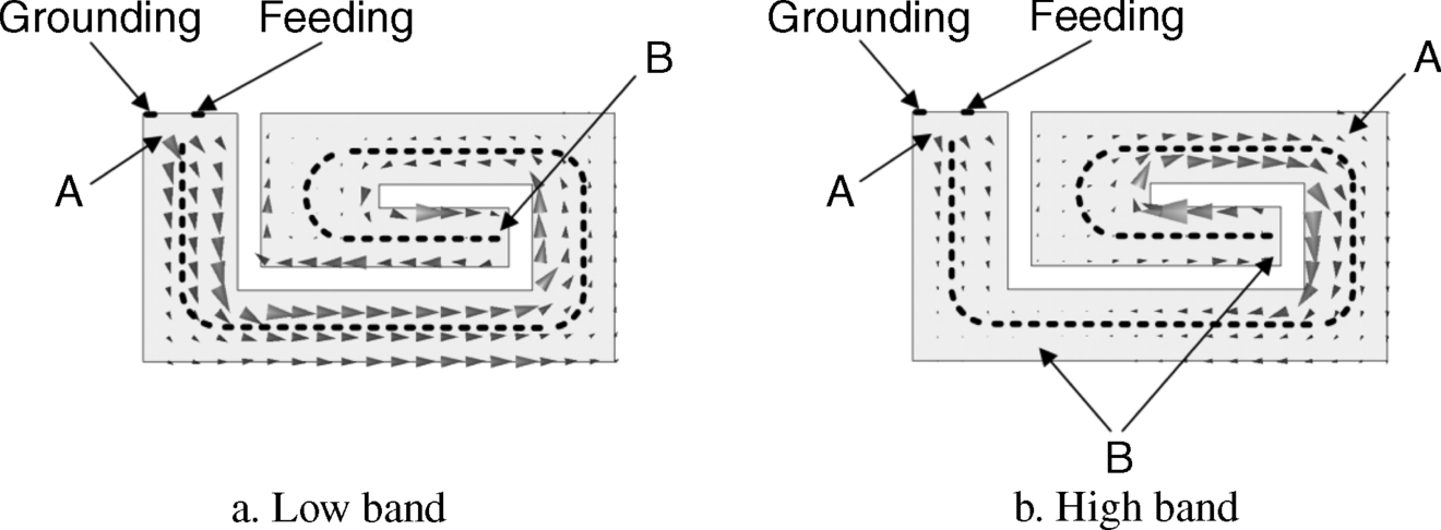
The current distributions of a “normal” PIFA antenna at both low and high bands are illustrated in Figure 4.25. The dashed lines in Figure 4.25 are the significant paths. At the low band, the current distribution along the critical path is more like a quarter-wavelength monopole. The current reaches its maximum at point A, which is around the feeding point. At point B, the current decays to zero.
Figure 4.25 Current distributions of a “normal” PIFA

In the high band, the current is more like a dipole along the critical path. It has the maximum in the middle, which is marked by point A. At both ends, which are marked as point B, the current decays to zero. As we know, a monopole antenna is not able to resonate when the antenna length is half of an effective wavelength, because its port impedance is too high to be matched. On the other hand, unlike a monopole, which is fed from one end of a radiator, a high-band patch mode is accessed from the middle, which explains why it has a decent impedance matching.
Although with regards to antenna tuning, a “normal” PIFA and a “small” PIFA are quite similar, their current distribution is totally different. Shown in Figure 4.26 are current distributions of a “small” PIFA antenna. The critical current paths of a “small” PIFA antenna at both bands are the same. At the lower band, the current along the critical mode is similar to a monopole, which has the peak current at point A and zero at point B. At the higher band, the total critical path corresponds to the third order mode, which is three-quarter wavelength. There are two peak current spots and two zero current spots. One might wonder, should the resonant frequency of the third order mode be three times its basic mode? To explain that, we need to recall the technique we discussed in Section 3.1.2.2. There, by adjusting the pitch of a helix, the resonant frequency of the third order mode can be tuned in a wide range. Similarly, the third order mode of a “small” PIFA antenna can also be tuned to where we want.
Figure 4.26 Current distributions of a “small” PIFA
Although mathematical formulas are given in many papers or books to calculate resonant frequencies of different bands, sometimes we do not need them. There are so many unknowns when designing an antenna for a real device, no formula can give an accurate prediction. The best way is to find out what the effect of each parameter is, then tune the antenna accordingly.
4.2.3 Multi-Band PIFA with Separate Branches
When the antenna area is big enough, a better design approach is to use two independent branches to cover low and high bands separately. The antenna shown in Figure 4.27 a is such an example. The antenna's size is 60 mm∗25 mm. The ground's size is 60 mm∗120 mm. The antenna is divided into two branches by the grounding strip. In Figure 4.27 a, the feeding strip is located on the side of longer branch. This arrangement is more favorable to the performance of the lower band.
Figure 4.27 A large PIFA

As the two branches are far apart, the responses at the low and high band are decoupled. The tuning process of this antenna is quite easy. When designing a large antenna, the first step is to adjust the length of both branches to get the resonances at the expected bands. Then by tweaking the distance between the feeding strip and the grounding strip, the matching at the lower band can be tuned. The final step is to design a matching circuit as shown in Figure 4.27 b to obtain a good matching at the higher band.
Shown in Figure 4.28 is the simulated reflection coefficient of the large PIFA antenna. By comparing this result with results shown in Figures 4.16 and 4.24, it is clear that the antenna has a wider bandwidth at both bands. As a rule of thumb, a larger antenna area is always better, which gives more design options and it is easier to achieve better performance.
Figure 4.28 Reflection coefficient of the large PIFA antenna
4.2.4 Multi-Band PIFA with Parasitic Element
There are many ways to expand PIFA antennas' bandwidth, which include using one slit with branches or multiple slits. PIFA variants using those techniques are too many to be enumerated in this book. Interested readers can find some enlightening examples in Professor Wong's book [1]. The technique we are going to discuss here uses the parasitic element.
Shown in Figure 4.29 is a PIFA with a parasitic element. The parasitic element is electrically connected to the ground through a metal strip. There is no direct connection between the main radiator and the parasitic radiator. However, they are electromagnetically coupled.
Figure 4.29 PIFA with parasitic element

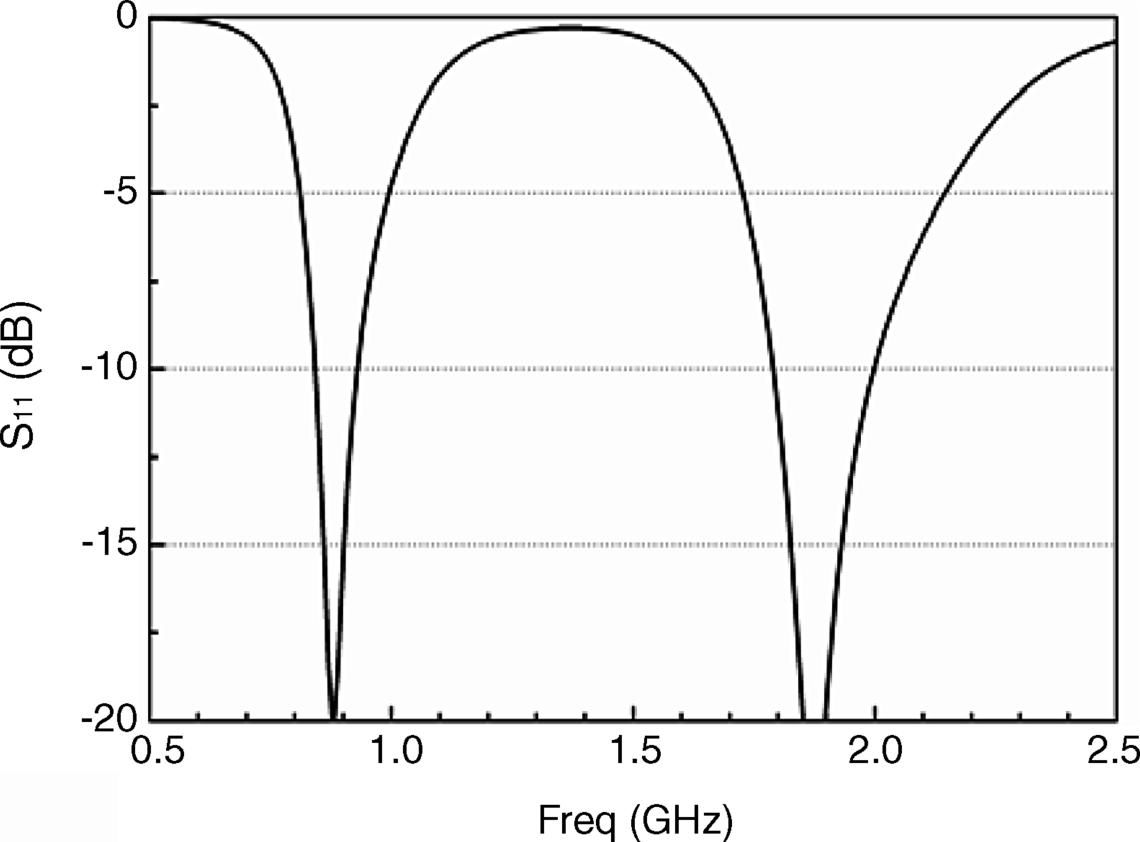
Shown in Figure 4.30 is the simulation result of a PIFA with a parasitic element. Similar to a normal PIFA antenna, the main radiator generates two resonances, one at the lower band and one at the higher band. The parasitic element only resonates at the higher band. The parasitic elements can frequently be found in penta-band 3G phones, which normally require frequency coverage over 1710∼2170 MHz at the higher band. A quad-band 2G phone only needs to cover 1710∼1990 MHz.
Figure 4.30 Reflection coefficient of a PIFA with a parasitic element

In practice, the parasitic element is normally used to cover the highest band. As higher frequency means smaller parasitic radiator, this makes antenna design easier. The other reason for using parasitic elements at the highest band is an antenna's overall performance. With the existence of parasitic element, the efficiency of the main radiator might degrade from one-tenth of a dB to a few dB. By assigning the resonance of a parasitic element to the highest frequency, the adverse effect on the lower band can be mitigated.
4.2.5 Manufacturing PIFA Antenna
Regarding designing techniques for PIFA antennas, this is as far as this book will go. The aim of this book is to aid in jump-starting an antenna project. This book mostly focuses on the core principles of antenna designing. However, there are so many phones on the market, that if you do some reverse engineering, you can discover various elegant tricks. The book does not touch upon those advanced techniques. On the academic side, Professor Kin-Lu Wong is one of the most innovative scholars in the mobile antenna world. Professor Wong has written two books [1, 6][1, 6] that cover advanced techniques.
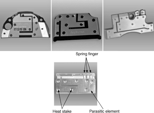
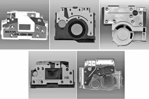
In this section, we are going to discuss the various processes of manufacturing PIFA antennas. The cheapest technology used to make an internal antenna is metal stamping. In production, a metal stamping antenna can be tuned quite quickly if the parameter needing to be adjusted is known and already included in the tooling design. The minimum number of parts necessary for a metal stamping antenna is two: one plastic carrier and one metal radiator. Multiple heat stakes are used to assemble the two parts together. As heat stakes are designed as a part of the plastic carrier, this feature is actually free. An assembly fixture is required to melt all the heat stakes and deform them into a mushroom shape. Shown in Figure 4.31 are some production metal stamping antennas. Most of the time, the volume available for antenna designing is irregular. To optimize the performance, an antenna must take full advantage of an irregular space. However, it is not difficult to see that those antennas still follow the basic design principles. Spring fingers are frequently used in metal stamping antennas as the contact feature. As spring fingers are formed from the same metal sheet which antennas are made of, they are also free. To meet the humidity and other environment requirements, spring fingers must be gold plated. To cut down on the manufacturing costs, a selective gold plating process can be used to minimize the plated area.
Figure 4.31 Metal stamping technology (Reproduced with permission from Shanghai Amphenol Airwave, Inc.)
At the dawn of internal antennas, dedicated volumes were reserved for antenna designing. With the continuous shrinking of mobile devices, eventually antennas have had to co-exist with other components, such the microphone, the speaker, the camera, and so on. Shown in Figure 4.32 are some samples of integrated antennas. If one is putting other components underneath an antenna, they must be RF isolated. Take the speaker as an example. There are two lead lines out of a speaker. Both of them must be isolated by inserting series inductors into signal paths.
Figure 4.32 Integrated antenna with other components (Reproduced with permission from Shanghai Amphenol Airwave, Inc.)
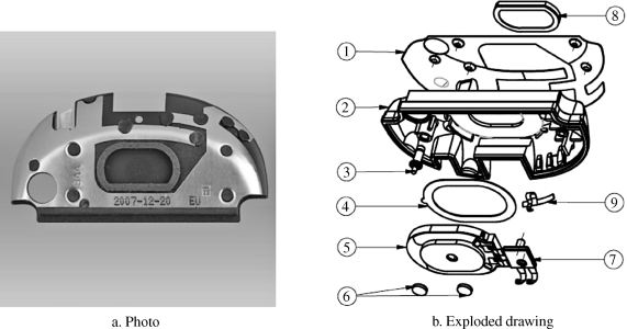
Normal metal stamping process can only bend metal sheets, so all the antennas shown above are not truly three-dimensional. They are either composed of multiple flat surfaces, or combinations of flat and cylindrical surfaces. The deep draw process can manufacture a true three-dimensional metal radiator. Shown in Figure 4.33 is an antenna made by the deep draw process. This antenna is also an integrated antenna. The exploded drawing is shown in Figure 4.33 b. Only parts #1 and #2, which are the metal radiator and the plastic carrier respectively, are destined for the antenna functionality. All the other parts are intended for the functionality of the speaker.
Figure 4.33 3D metal stamping integrated antenna (Reproduced with permission from Shanghai Amphenol Airwave, Inc.)
Compared with metal stamping technologies, the flex circuit technology has better consistency but it is a little more expensive. In many state-of-the-art designs, the antenna volume is quite tight, which means the performance margin is relatively slim. Because flex antennas have better consistency, they also have better yield rate. The flex itself cannot provide connecting features, some extra parts, such as metal spring fingers or pogo pins, are needed.
The flex technology is not a true three-dimensional technology, see Figure 4.34. A flex can only wrap around a combination of two-dimensional surfaces. The most advanced and also the most expensive technologies in antenna manufacturing are double-shot molded interconnect device (DS-MID) and/or laser direct structuring (LDS). They have the best consistency, because the antennas are part of the plastic structure instead of separate parts. Both of them are based on a technique called selective metallization. The DS-MID process begins with the application of a shot of plateable thermoplastic resin into an injection-mold cavity. Next, the cavity is changed and a second shot of nonplateable thermoplastic resin is molded around the first shot to create a circuit pattern from the plateable material. These parts are then plated with a layer of copper. The DS-MID takes the longest lead time, because any modification to the antenna pattern requires tooling changes. The LDS is a relatively new process. The thermoplastic resin used in LDS process is nonplateable after the molding process and can be transformed to plateable by using a laser beam to activate it. The LDS process literally draws the antenna pattern on to the plastic. The pattern can be adjusted quite easily by uploading a new pattern file to the laser. Similar to the DS-MID, a plating process is required to deposit copper onto the part's surface. Shown in Figure 4.35 is an antenna made by the DS-MID process.
Figure 4.34 Flex technology (Reproduced with permission from Shanghai Amphenol Airwave, Inc.)

Figure 4.35 Antenna made by DS-MID technology (Reproduced with permission from Shanghai Amphenol Airwave, Inc.)

When choosing from different antenna technologies, an engineer needs to take into consideration cost, consistency, and lead time. It is always a good idea to consult experienced engineers and antenna manufacturers.
A PIFA antenna implies that there is a ground plane underneath the antenna element. When a phone with a PIFA antenna is used in a talking position, the ground is sandwiched between the head and the antenna. The ground functions as a shield, which can direct some of the near field energy away from the head, thus decreasing the radiation to the user's brain. However, from an antenna design point of view, the antenna bandwidth can be significantly expanded if the ground can be removed. When the ground is removed, the antenna is no longer a PIFA, it is called a folded monopole antenna.
For all phones with PIFA antennas, in my experience, the antennas are on the top of the phone. The “ancient” wisdom is that by putting an antenna on the top of a phone, the hand effect on the antenna can be mitigated. When the phones became thinner and smaller, the volume left for antenna also become too small to fulfill the bandwidth requirement. An obvious way to ease the pressure on antennas is by using monopole antennas. However, a monopole antenna cannot be placed on the top of a phone, because as there is no ground acting as the shield between the user's head and the antenna, the radiation to user's brain would be too high. A logical way of working around this is to put the antenna at the bottom of a phone. As the bottom of a phone never comes into contact with people's head, this solution allows the phone to pass the radiation safety regulations. In my experience, I have proposed this kind of solution in two projects and been rejected twice. The reason for rejection is that if we put the antenna at the bottom, the user's hand will always cover the antenna, thus degrading the antenna's efficiency. I am sure that due to the pressure on antenna designing, many antenna engineers were starting to think about bottom-installed monopole antennas at that time.
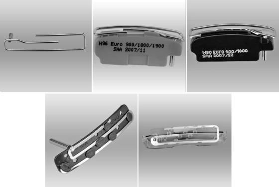
Everything changed in 2004, when the Motorola Razor was revealed, as shown in Figure 4.36. The Motorola Razor is a de facto grand slam. More than 20 million Razors and its derivates have been sold worldwide. I have to admit that I had never imagined that by putting an antenna at the bottom, industry engineers could have so much design freedom. The success of the Razor started the new trend for the ultra-slim phone. Nokia, Samsung, and so on, all released their own models which looked just like Razor's cousins, and all of them have a bottom-installed internal monopole antenna.
Figure 4.36 Motorola Razor (Reproduced with permission from Motorola, Inc. All rights reserved.)

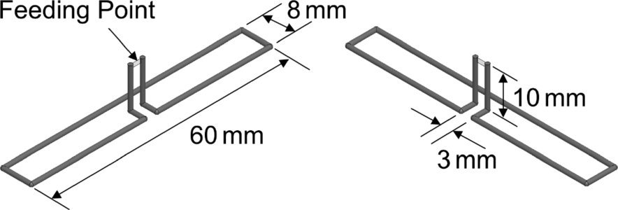
Figure 4.37 depicts an internal monopole antenna. The antenna protrudes over the edge of the ground plane. The antenna is composed of two pieces of metal wires. The thicker wire makes the connection to the feeding spring finger on the PCB board. The thinner wire is attached to the thicker wire by a welding process. The thinner wire is divided into two branches by the thicker wire. The shorter branch resonates at the higher band and the longer branch resonates at the lower band. If comparing an internal monopole with the dual-branch multi-band stubby antenna discussed in Section 3.1.2.1, we can see that although they have totally different form factors, they are pretty much the same from the electrical point of view.
Figure 4.37 Internal folded monopole antenna

Shown in Figure 4.38 is a simulation model of a folded monopole antenna. The area of ground is 100 mm∗50 mm. The dimension D, which is the length of the thick wire and also is the distance between the antenna element and the edge of the ground, is the decisive factor in an antenna's bandwidth.
Figure 4.38 Dimensions of a sample internal monopole antenna

Shown in Figure 4.39 are simulation results of folded monopoles with different dimensions D. When the D changes, the resonant frequencies at different bands will drift. The branches' lengths need to be tweaked accordingly to compensate for the frequency drift. In Figure 4.39, when the D is 5 mm, the antenna element is too close to the ground, thus inducing a strong current on the horizontal edge of the ground. This induced current is always in the opposite direction to the current on the antenna element. The radiations of both currents cancel each other out, so the antenna cannot radiate well. When D increases, the bandwidths of both low and high bands increase. When D increases from 10 to 15 mm, the bandwidth increases a little at the higher band but quite significantly at the lower band. This is because the impact of the gap is measured by how much wavelength it is instead of the absolute dimension. At the lower band, the wavelength is longer, so it is always more difficult to achieve good performance at the lower band in a constrained space.
Figure 4.39 Internal folded monopole with various D

Shown in Figure 4.40 is the impact of the shorter branch. The length of the shorter branch mostly affects the higher band. By increasing or decreasing the shorter branch, the resonant frequency of the higher band can be tuned lower or higher. For the example shown in Figure 4.40, when adjusting the branch length by 2 mm, the frequency changes roughly 60 MHz.
Figure 4.40 Internal folded monopole, variation in the shorter branch, D = 10 mm

The length of the longer branch affects the resonant frequencies of both low and high band. As shown in Figure 4.41, when decreasing the longer branch, both resonant frequencies shift higher.
Figure 4.41 Internal folded monopole, variation in the longer branch, D = 10 mm

Before tuning any antenna, it is important to have a clear understanding of what the impact of each dimension is. With that knowledge, it is easy to decide the best tuning procedure and whether an iterative tuning is necessary. For the antenna shown in Figure 4.38, if we tune the higher band first, then an iterative procedure has to be used. The appropriate tuning sequence should be tuning the lower band first. We can start with an antenna whose both branches are a little bit longer, then gradually trim off the longer branch. After correctly tuning the lower band, double check the higher band's resonance to make sure it is lower than what we need. The final step is to gradually trim off the shorter branch until the higher band is well tuned.
The antenna shown in Figure 4.38 is a simplified model. In reality, when there is a hands-free speaker, microphone, shielding box, battery, and other components around the antenna, you may find the both branches have an effect on both bands simultaneously, and an iterative tuning process has to be used in such circumstances.
Shown in Figure 4.42 are some production internal monopole antenna. The manufacturing techniques used are a little bit different. However, they are pretty much the same from the electrical point of view.
Figure 4.42 Production internal monopole antennas (Reproduced with permission from Shanghai Amphenol Airwave, Inc.)
Loop antennas are one of the oldest antennas. In 1886, H. Hertz demonstrated the first wireless (spark) communication system which verified the existence of the electromagnetic wave. In the experiment set-up, a dipole antenna was used as the transmitter and a loop antenna was used as the receiver. Loop antennas are classical antennas and are explained in most antenna textbooks [7–11]. There are electrical small loop antennas and electrical large loop antennas, and a detailed theoretical analysis of both antennas can be found in textbooks [7]. Only electrical large loop antennas can be used in the cellular communication. Similar to a folded monopole antenna, a loop antenna also needs to be installed on the bottom of a device to avoid high radiation to a human brain.
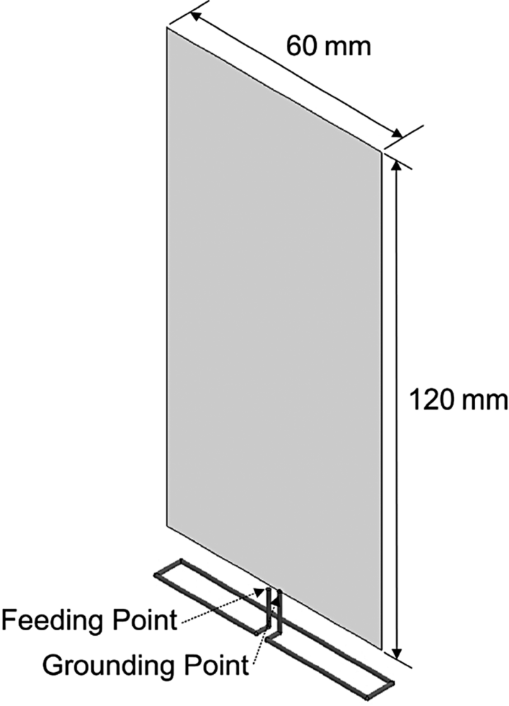
Shown in Figure 4.43 is a loop antenna. The shape of this loop antenna is a little bit abnormal, because we want to use it in the following studies. The shape of the loop antenna slightly affects the resonant frequency, other than that, it is a good example without losing generality. The loop of the antenna shown in Figure 4.43 is quite narrow, so it sometimes also is categorized as a folded dipole antenna. We should obtain the same result no matter which analytical method is used.
Figure 4.43 Oblique views of a loop antenna
The loop antenna shown in Figure 4.43 has a dimension of 60 mm∗8 mm, which is the same as the folded monopole antenna discussed in the last section. The antenna is fed by a parallel transmission line, which is perpendicular to the antenna plane. The feeding point is at the end of the transmission line.
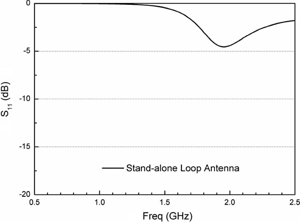
Shown in Figure 4.44 is the simulated reflection coefficient of the stand-alone loop antenna. The first resonance appears around 2 GHz, which is about two times higher than the folded monopole antenna whose longest branch is even shorter than the loop antenna. The reason is that the first resonance of a stand-alone loop antenna appears when the loop length equals one wavelength. A folded monopole can resonate when it is a quarter of a wavelength.
Figure 4.44 Reflection coefficient of a stand-alone loop antenna
Shown in Figure 4.45 is the current distribution of a one-wavelength loop antenna. There are two half-wavelength standing-wave currents on the loop. The standing-wave nodes are on both sides of the loop. On a straight line, the currents at both side of a standing-wave node are in opposite directions. A loop antenna is bent at the node, so two standing-wave currents are actually flowing in the same direction and can effectively radiate. A loop antenna must be excited differentially, which means at the feeding point, the currents on both sides are always in the opposite direction. As shown in Figure 4.45, the currents on the left and right side flow into and out the source respectively.
Figure 4.45 Current distribution of a one-wavelength stand-alone loop antenna

The reflection coefficient of a stand-alone loop antenna is not very good. The impedance of a stand-alone loop antenna is around 300 Ω, about four times a half-wavelength dipole antenna. Detailed analysis is omitted here and can be found in textbooks [7]. Beside the base frequency f0, a stand-alone loop antenna also resonates at integer multiples of f0. If the first resonance is at 2 GHz, the second and third resonances should appear around 4 GHz and 6 GHz.
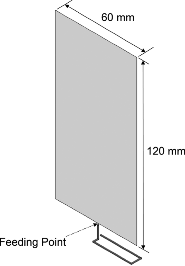
Shown in Figure 4.46 is a bottom-installed loop antenna. The dimensions of the antenna were illustrated in Figure 4.43. The ground plane has a dimension of 100 mm∗60 mm. Unlike a stand-alone loop antenna, the loop antenna shown in Figure 4.46 is unbalanced fed. One end of the loop antenna is connected to the ground plane and the other end serves as the feeding point.
Figure 4.46 Bottom-installed loop antenna
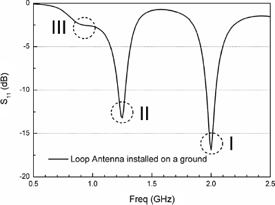
Shown in Figure 4.47 is the simulated reflection coefficient of a bottom-installed loop antenna. By comparing Figures 4.44 and 4.47, significant difference can be observed. The resonance (I) shown in Figure 4.47 can be explained by the one-wavelength loop antenna mode. Resonances (II) and (III) do not even exist on a stand-alone loop antenna, so they must have something to do with the ground plane.
Figure 4.47 Reflection coefficient of a bottom-installed loop antenna
Shown in Figure 4.48 is a bottom-installed monopole antenna. The monopole antenna is made by splitting the loop antenna and removing half of it. Apart from the antenna, everything else in the fixture is identical to the one shown in Figure 4.46. As we know, a monopole antenna is only half of the radiator and the ground functions as the other half.
Figure 4.48 Bottom-installed monopole antenna
Shown in Figure 4.49 is the simulated reflection coefficient of a bottom-installed monopole antenna. Compared with results shown in Figure 4.47, the resonance (I) has disappeared but resonances (II) and (III) are still preserved. For a monopole antenna, the resonance (II) is introduced by the monopole itself and resonance (III) is the contribution of the ground plane. If you want to verify the root cause of those two resonances, you can vary the length of either the monopole or the ground plane separately and the resonant frequency will shift accordingly.
Figure 4.49 Reflection coefficient of a bottom-installed monopole antenna

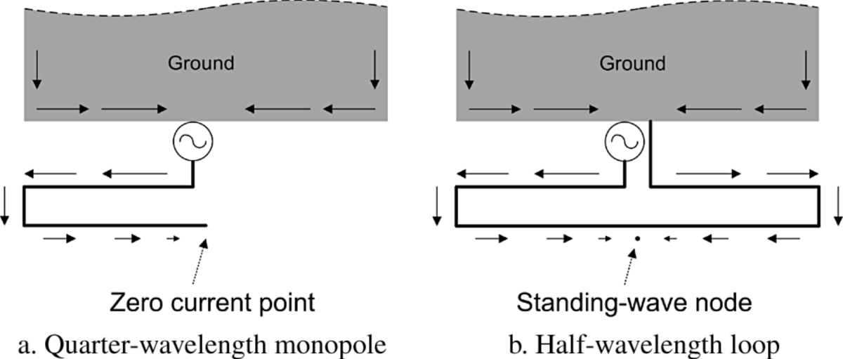
Based on Figures 4.47 and 4.49, it is quite safe to assume that a loop antenna functions as a monopole antenna when it is half a wavelength long and installed on a ground plane. Shown in Figure 4.50 are the current distributions of a quarter wave monopole antenna and a half-wavelength loop antenna when installed on a ground plane. For both antennas, the current distributions on the ground plane are pretty much the same. Some people might categorize the current on the half-wavelength loop as a common-mode. It is fine as long as we remember such a common-mode cannot exist without a ground plane. For any signal source, the sum of all currents flowing in and out is always zero. For a half-wavelength dipole antenna or a one-wavelength loop antenna, the currents on both sides are always in opposite directions, so they satisfy the condition of zero sum current. For a quarter-wavelength monopole antenna or a half-wavelength loop antenna, because the sum of the currents on the antenna element is not zero, there must be a ground which provides a path for the opposite current. With the assistance of a ground, a loop antenna can also resonate when it is odd multiples of half a wavelength.
Figure 4.50 Current distributions of a monopole and a loop
By utilizing the half-wavelength, one-wavelength and/or one and a half wavelength modes, multi-band antennas have been designed and reported [12–15]. So far, in my experience, the best one is reported in [13], which achieved a VSWR better than 3 : 1 at 822–964 MHz and 1570–2260 MHz. The antenna volume is 60 mm∗10 mm∗4 mm.
Some articles or companies might claim that a loop antenna has a localized current distribution, thus has much less radiation to human brains and is immune to the loading effect when the ground plane is held by hand. This claim is only partially true. As we have demonstrated, when the antenna is working in the one-wavelength mode, the antenna is differentially fed, thus has limited current on the ground. In this circumstance, the claim holds well. However, when the antenna is working at the half-wavelength mode, which normally corresponds to the 900 MHz band, the ground plane becomes the main radiator and a loop antenna is really no better than its monopole counterpart from the radiation safety point of view. Similarly, for one and a half-wavelength mode, the claim is also invalid.
Just as its name implies, any ceramic antenna is made of ceramic. There are mainly three kinds of antennas which are made of ceramic. The first is often referred as the dielectric resonator antenna [16–21]. A dielectric resonator antenna normally has a cylinder or a cuboid form factor. The ceramic block becomes a good radiator when resonant modes, such as TM10δ, TM10δ, and so on, can be effectively excited. The air–dielectric boundary of an antenna can sustain the resonant standing wave in the ceramic, so no metal is needed. However, at the cellular communication frequency, a dielectric antenna is too chunky to be used in hand-held devices.
The second kind is the ceramic patch antennas [22–25]. Those antennas can generate circular polarized radiation patterns and are normally used in satellite applications, such as GPS (global positioning system) and XM satellite radio. Although ceramic patch antennas are widely used in hand-held GPS navigators, they are seldom used in cellular phones. Ceramic patch antennas do give better performance than their counterparts. However, due to the size consideration, most cellular phones still use other types of antennas, such as IFA antennas, to cover the GPS frequency band.
The third kind of ceramic antenna is the one widely adopted in the mobile industry. From an electromagnetic technology point of view, these ceramic antennas are not really utilizing any brand new technology. All of them can be labeled as monopole, IFA, and so on. All antennas introduced in this section belong to the third category.
The main reason for the introduction of ceramics into antenna design is size considerations. Most material used in ceramic antenna design has high relative permittivity, which ranges from a few tens to more than 100. With the higher relative permittivity, an antenna's size gets smaller and its bandwidth also shrinks accordingly. Thus the tolerance of ceramic's relative permittivity must be well controlled. Fortunately, good tolerance is one of the advantages ceramic material provides. The ceramic used in antenna design also has very little loss, which is a critical merit to guarantee good efficiency when an antenna is exceedingly small. Unlike the plastic support used in other types of antenna, ceramic can sustain the temperature in the soldering oven. Most ceramic antennas are designed using surface-mount technology (SMT) and are compatible with the standard SMT soldering process. Unlike other antennas, ceramic antennas do not require a dedicated manual assembly step, they can be handled like any other components, such as capacitors, resistors, or integrated circuits.
4.5.1 Monopole-Type Ceramic Antenna
In a state-of-the-art cellular phone, there is most likely more than one antenna. The antenna used for the voice communication is normally referred to as the primary antenna. All other antennas are referred to as auxiliary antennas, such as GPS, Bluetooth, or wireless LAN (WLAN) antennas. Almost all ceramic antennas are narrow band antennas. Due to their limited bandwidth, they are mostly used as the auxiliary antennas. Some companies have proposed using ceramic antenna as the main antenna but this has not been popular due to the performance issue.
For the primary antenna, the performance is critical, because users perceive the quality of a phone mostly by its sound's quality. If all other phones can make a call in one spot but one phone cannot, the reputation of the phone will be badly damaged. On the other hand, auxiliary antennas are used in applications which are not critical. People do not expect seamless coverage for those applications in the same way they do for voice communication. Thus, the performance requirements for auxiliary antennas are not that stringent. A primary antenna must be custom-made as optimized for each phone model to squeeze the last drop of the performance from the available physical space. On the other hand, ceramic antennas are designed and built as off-the-shelf components. The main consideration is reuse and standardization.
Shown in Figure 4.51 are two types of monopole ceramic antennas. One is made by Panasonic, which is a coil-type antenna. The other one is made by Johanson Technology, which adopts the multi-layer technology. The plating and laser etching process are involved in making coil-type ceramic antennas. A small piece of ceramic block is plated with metal first. Then a procedure, which is analogous to making a screw, is used to laser etch a spiral slot on the metal layer. The end product is a metal coil rounding around a ceramic block. The axis of the coil aligns with the longest axis of the ceramic block. This process is quite similar to the one used in making metal film resistors. The advantage of this process is that the resonant frequency can be adjusted quite easily. The number of turns of a coil, which corresponds to the resonant frequency, can be conveniently adjusted by reprogramming the laser fixture.
Figure 4.51 Monopole-type ceramic antennas (not to scale) (a) (Reproduced from Panasonic Corporation and (b) Reproduced with permission from Johanson Technology, Inc.)

Multi-layer type ceramic antennas can be made by either the standard chip capacitor process or LTCC (low temperature co-fired ceramic) technology. From the electromagnetic point of view, both processes are the same. They stack multiple layers of meander lines and make an interconnection between layers. The end product is a three-dimensional meander line. The relation between a coil ceramic antenna and a multi-layer ceramic antenna is analogous to a helix stubby antenna and a meander line stubby antenna.
A monopole ceramic antenna is still a monopole, which means its relative position to a ground plane must be correctly arranged. Shown in Figure 4.52 are two incorrect ways of placing monopole type ceramic antennas. Why they do not work well can be explained by the image theory. For both placements, the image current on the ground is in the opposite direction to the current on the antenna, and the separation between the two currents is too small. The radiation forms of the respective currents cancel each other in the far field, and that prevents the antenna from radiating. If measuring the reflection coefficient of either antenna shown in Figures 4.52 a or b, we might not observe any resonance at all.
Figure 4.52 Wrong ways of placing monopole-type ceramic antennas

Shown in Figure 4.53 are three correct ways of placing monopole-type ceramic antennas. The one shown in Figure 4.53 a is the best scenario, where the antenna is vertically placed on the edge of ground plane. All the copper layers on the top portion of PCB are clearly outside. When using this kind of layout, the antenna is identical to an external stubby antenna except it is concealed from the cosmetic point of view. Many companies use this kind of antenna placement when measuring the antenna's performance.
Figure 4.53 Correct ways of placing monopole-type ceramic antennas
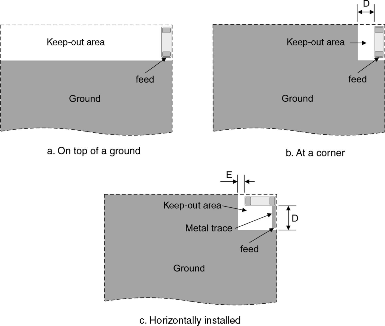
In Figure 4.53 a, the keep-out area means no components or traces can be routed in that area, and that is quite a waste, especially for a cellular phone, where it is always a struggle for space to fit in all the components. Shown in Figure 4.53 b is a real scenario. The keep-out area has significantly shrunk. In this kind of layout, the dimension D, which is the distance between the antenna and the vertical edge of the ground, is the critical parameter. By decreasing D, the keep-out area can be smaller, however, the antenna's bandwidth and efficiency are sacrificed. So it is an engineering trade-off again, you have to pay something to gain something.
Shown in Figure 4.53 c is another frequently used lay-out. The antenna is horizontally placed and a segment of metal trace is used to feed the antenna. In this arrangement, both dimensions D and E are critical parameters. The larger the gap, the better the performance. When using a ceramic antenna, it is always easier to shift an antenna's resonant frequency down than shift it up. So some ceramic antennas are purposely made with a resonant frequency a little bit higher than the target band. When using this kind of antenna, a small segment metal trace on a PCB is required to tune the frequency down.
Shown in Figure 4.54 is the measure response of a typical WLAN chip antenna. The antenna's model number is 2450AT43A100 and it is made by Johanson Technology. It has a −10 dB reflection coefficient bandwidth of 300 MHz. The antenna is 1.2 mm tall, 7 mm long, and 2 mm wide.
Figure 4.54 Performance of Johanson Technology 2450AT43A100 (Reproduced with permission from Johanson Technology, Inc.)

For all monopole ceramic antennas, the ground around and underneath the antenna must be removed. A monopole ceramic antenna itself can be quite small. It is normally around 1 mm tall, a few millimeters wide, and less than 10 mm long. Most companies are often proposing those antennas as small footprint solutions. As antenna designers, we need to be very careful here. If an antenna claims a footprint of 2 mm∗10 mm and we request an antenna area accordingly, we will soon find ourselves stuck in a bad situation. We must not forget to include the keep-out area. As a rule of thumb, it is always much easier to get antenna space at the start of a project rather than at the end.
4.5.2 IFA-Type Ceramic Antenna
Shown in Figure 4.55 is an IFA ceramic GPS antenna made by Murata Inc.©. To increase the effective length of the antenna, the metal trace is routed into a U shape at the top surface of the ceramic block. On the bottom of the antenna, there are three solder pads or terminals. The antenna is fed from terminal (1). Terminal (1) on the bottom is connected to the antenna on the top through the sidewall. However, there is no galvanic contact between terminal (1) and the antenna. There is a gap between them on the sidewall. The gap functions as a series capacitor which is a part of the matching network. The other matching component required is a shunt capacitor installed on a PCB. If we remove these two capacitors, it is easy to see that without any matching the antenna impedance is inductive and is on top side of the Smith Chart. Terminal (2) is the grounding pad, through which the antenna is connected to the system ground. Terminal (3) of the antenna is a tuning pad. This pad is DC floating but electromagnetically coupled to the antenna. By connecting a capacitor or an inductor, the effective loading of an antenna can be changed, thus fine tuning of the antenna can be achieved.
Figure 4.55 IFA ceramic GPS antenna (Reproduced from Murata Manufacturing Co. Ltd.)

An IFA ceramic antenna is also marketed as an over-ground chip antenna solution. Based on the basic principle of image theory, we know that an antenna must be adequately separated from the ground to radiate effectively. The antenna shown in Figure 4.55 is 4 mm tall, which is about four times taller than its counterparts of monopole ceramic antennas. As an example of such antennas, a Murata WLAN IFA ceramic antenna (ANCG12G44SAA145) has a −4.5 dB reflection coefficient bandwidth of 84 MHz. The antenna is 3.8 mm tall, 9.8 mm long, and 2 mm wide. If comparing with a monopole antenna by the absolute size of the ceramic block, an IFA ceramic antenna is significantly bigger and its bandwidth is a lot narrower. However, an IFA ceramic antenna does not require a keep-out area on the PCB, so the effective antenna space it requires is actually less than a monopole.
In practice, the PCB area around antenna can be safely used to lay out small components. However, be cautious when placing large metal components, such as the shield box, battery, and so on, around the antenna. The antenna's performance will be significantly degraded when it is immediately adjacent to a metal object.
4.5.3 Loop-Type Ceramic Antenna
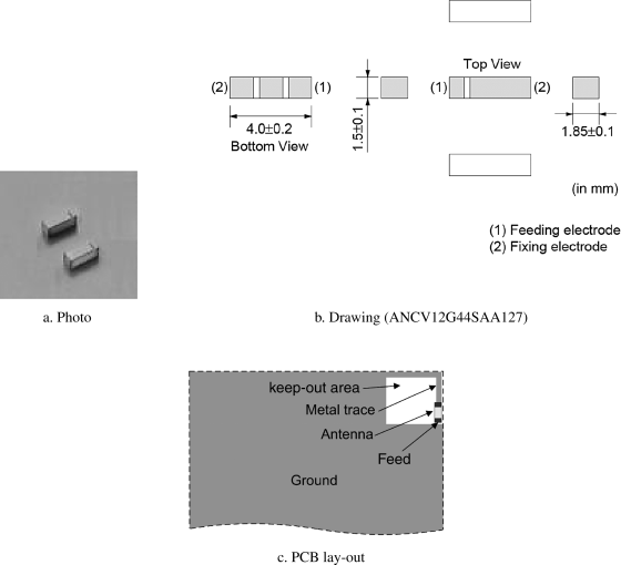
Shown in Figure 4.56 is a loop ceramic antenna. The antenna is 1.85 mm tall, 4 mm long, and 1.5 mm wide. As illustrated in Figure 4.56 b, all gray areas are metalized surface. The two long sidewalls are cleared of metal. At the bottom of the antenna, two slits are cut to form two solder pads. On the top of the antenna there is one slit. It might seem small, but be careful, because the “antenna” is actually only a component of a loop antenna. Shown in Figure 4.56 c is a PCB layout of this antenna. The effective antenna is the loop around the keep-out area. The ceramic chip antenna functions more or less like a series capacitor. However, the ceramic chip is comparably big, so it does play a role in the antenna's radiation. The ceramic chip is made of high dielectric material that effectively decreases the overall size of the loop antenna. The chip is composed of low loss dielectric and has a high concentration of electromagnetic field, which improves the radiation efficiency. By cutting slits on a ceramic block, the capacitance of the chip can be better controlled than a multi-layer ceramic capacitor, which improves frequency stability.
Figure 4.56 Loop ceramic WLAN antenna (Reproduced from Murata Manufacturing Co., Ltd.)
The impedance of a loop-type ceramic antenna is affected by the loop shape and position. In most circumstances a shut matching component is needed to achieve good matching. For the WLAN antenna chip (ANCV12G44SAA127), the −5dB reflection coefficient bandwidth given in the datasheet is 84 MHz.
In conclusion, of monopole, IFA and loop ceramic antennas, the one that occupies the least PCB area is ceramic IFA antennas. For monopole and loop ceramic antennas, there is a design trade-off between required PCB area and the antenna's performance. There are different variants of ceramic antennas in the market, but in reality they can be analyzed by the way we are familiar with. After all, the ceramic antenna is not a startling new innovation, it is only a different way of manufacturing antennas.
4.6 Multi-Port Internal Antenna Module
For all the antennas we have discussed, no matter whether external or internal antennas, they are all single port antennas. With the progress of integrated circuit (IC) technology, the size of the IC shrinks quite a lot; in the meantime, more and more functionalities can be integrated into a single chip. Antennas are now occupying a considerable portion of the available phone volume. In these circumstances, it really is a luxury to ask for dedicated volume for each individual antenna. As a consequence, several antennas have to be squeezed to form a multi-port antenna module and share the same physical space. In this section, a dual-port antenna is used to demonstrate some considerations when designing a multi-port antenna module.
With the rapid growth of the mobile communication industry, increased functionality has been integrated into a single mobile device. A CDMA phone sold in the USA has to cover at least three bands, the cellular band (824–894 MHz), the GPS band (1575 MHz), and the PCS band (1850–1990 MHz). Many CDMA phones also cover a fourth band, the Bluetooth band (2400–2484 MHz).
Based on current popular RF chipset architectures, the best antenna solution to cover the four bands of cellular, GPS, PCS, and Bluetooth needs three independently fed antennas. One antenna operates over cellular and PCS bands, one on the GPS band, and the third one on the Bluetooth band. Ideally, all three antennas can be separate enough to guarantee good isolation between them and each antenna can be placed at a separate corner on a phone. However, from the system of point, it is preferable to have all the antennas packaged into one single module. Because with only one module, the logistic process is slimmer and the PCB routing is also easier.
When squeezing three antennas into a compact volume, the mutual coupling among antennas will degrade antenna efficiency and also make it very difficult to achieve good isolation. It is an attractive trade-off to integrate some antennas into one to form a multi-band antenna.
In the past, due to the chipset architecture, single port tri-band antennas were used to cover cellular, GPS, and PCS bands. The GPS module used in those systems did not work with cellular or PCS modules simultaneously, and thus a switch was typically used to connect the tri-band antenna to different transceivers. Today, most new generation GPS modules are stand-alone solutions, and require GPS and cellular or PCS to work at the same time. Due to the high transmitting power at cellular and PCS bands, using a tri-band antenna and a triplexer to cover three bands cannot achieve the required GPS sensitivity (free space isotropic sensitivity of −145 dBm). Thus the GPS antenna has to use a different antenna port from the cellular and PCS port.
There is a similar issue when integrating the cellular, PCS, and Bluetooth bands into one antenna. Cellular and PCS transceivers normally transmit above 23∼25 dBm and Bluetooth transmits around 0 dBm. To achieve the required sensitivity, a diplexer with sharp roll-off and higher out-band rejection has to be used. Considering the frequency domain proximity of the PCS band (1990 MHz) and the Bluetooth band (2400 MHz) edges, this scheme is also not used in cell phone design.
So a reasonable solution is to combine the GPS and Bluetooth antennas into one antenna. A Bluetooth transceiver transmits at a relatively lower power than cellular transceivers, and thus the out-band rejection requirement of a diplexer is reasonable. The GPS and Bluetooth bands are well separated in frequency, so the roll-off requirement is also easy to be achieved. Several off-the-shelf diplexers have the required specifications to separate these two bands inside the RF front end.
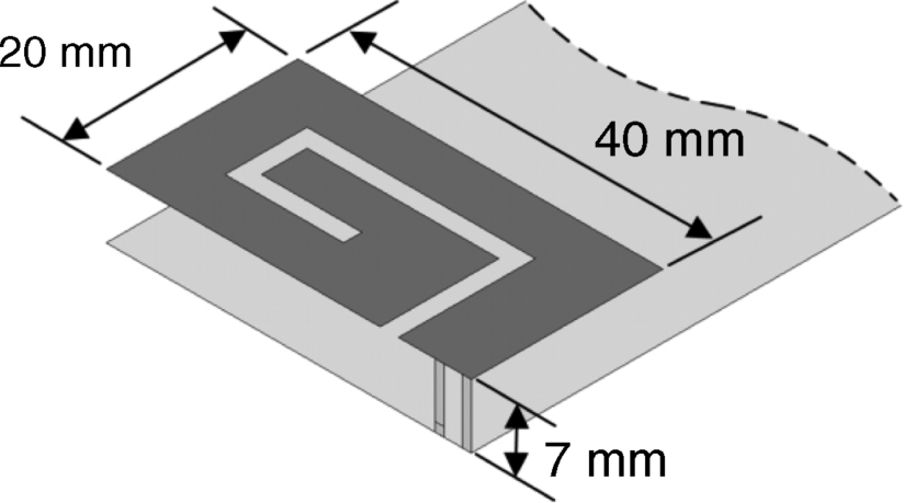
Shown in Figure 4.57 is the proposed dual-port quad-band antenna. It comprises one IFA dual-band cellular and PCS antenna and one dual-band GPS and Bluetooth ceramic chip monopole antenna. Figure 4.57 a shows the front view of the dual band IFA antenna. The size of the PCB (FR4) is 50 mm∗95 mm∗1 mm. The whole PCB is covered by copper except for 6 mm along the top edge. The dual-port antenna solution occupies a volume of 10.5 mm∗10 mm∗50 mm. The top of the IFA antenna is 2.5 mm away from the top of PCB, which increases the length of whole device to 97.5 mm. The IFA antenna has a consistent strip width of 1 mm. The critical dimensions of the IFA are L1, L2, S1, and H1. By changing the L1 and L2, PCS and cellular resonant frequencies can be tuned separately. By increasing S1, the bandwidth of PCS resonance can be increased. However, increasing bandwidth degrades isolation between the IFA antenna and ceramic antenna. By decreasing H1, the third resonant frequency of IFA antenna can be increased, but that decreases the impact of the IFA antenna on the Bluetooth band, at the expense of the IFA antenna's cellular bandwidth.
Figure 4.57 A dual-port quad-band antenna module L1 = 31 mm, L2 = 29 mm, L3 = 11 mm, L4 = 3 mm, S2 = 1 mm and H1 = 7.5 mm
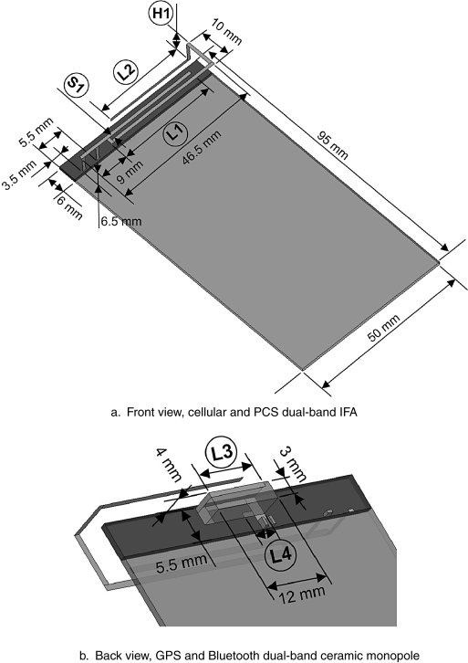
Figure 4.57b shows the GPS–Bluetooth dual-band ceramic IFA antenna. The dimensions of the ceramic block are 3 mm∗4 mm∗12 mm. The ceramic's dielectric constant is 20. The antenna is a monopole-type antenna. A 2.2 nH shunt inductor is used to match the impedance to 50 Ω. The ceramic antenna has a consistent strip width of 0.8 mm. There are two 2 mm∗3 mm solder pads on the antenna to make it surface mountable. The critical dimensions of ceramic antenna are L3 and L4. By changing L3 and L4, GPS and Bluetooth resonant frequencies can be tuned separately.
Figure 4.58 shows the measured VSWR of the dual-port quad-band antenna. The VSWR was measured with the unused port terminated by a 50 Ω load. The solid line is the response from the cellular and PCS port and the dashed line from the GPS and Bluetooth port. Band edges are marked on the graph with small circles. VSWRs of 3.5 : 1 and 3 : 1 were achieved on the cellular and PCS bands respectively. VSWRs of 1.2 : 1 and 2.5 : 1 were achieved on the GPS and Bluetooth bands respectively. Figure 4.59 shows the isolation between the two antenna ports. Isolation is better than 12 dB on cellular and GPS bands and better than 17 dB on the PCS and Bluetooth bands. Actually, the isolation in the cellular band still needs to be higher to avoid the cellular signal's jamming effect on the GPS receiver. An additional cellular band notch filter needs to be used on the GPS signal path after the GPS–Bluetooth diplexer.
Figure 4.58 Measured VSWR of the cellular and PCS port and the GPS and Bluetooth port

Figure 4.59 Measured isolation between the cellular and PCS port and the GPS and Bluetooth port
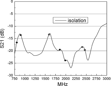
Figure 4.60 shows the efficiency measured in a 3D chamber. The efficiency was measured with the spare port terminated by a 50 Ω load. The efficiency is 33∼42% at the cellular band, 45% at the GPS band, 60∼90% at the PCS band, and 68∼81% at the Bluetooth band.
Figure 4.60 Measured efficiency of a dual-port dual-band antenna

Figure 4.61 shows the measured 3D radiation patterns. The GPS and Bluetooth ceramic antenna is on the front of PCB and faces the +X axis. The color map scale is from −15 dBi to 5 dBi. Patterns of cellular, GPS, PCS and Bluetooth are shown in Figures 4.61 a–d respectively.
Figure 4.61 Measured 3D radiation patterns

1. Wong, K.-L. (2003) Planar Antennas for Wireless Communications, Wiley-Interscience.
2. Arkko, A.T. (2003) Effect of ground plane size on the free-space performance of a mobile handset PIFA antenna. 12th International Conference on Antennas and Propagation, 2003. (ICAP 2003). (Conf. Publ. No. 491), vol. 1, pp. 316– 319.
3. Chan, K.H., Fung, L.C., Leung, S.W., and Siu, Y.M. (2006) Effect of internal patch antenna ground plane on SAR. 17th International Zurich Symposium on Electromagnetic Compatibility, 2006. EMC-Zurich 2006., pp. 513– 516.
4. Fujio, S. (2006) Effect of ground size on plate inverted-F antenna. IEEE International Workshop on Antenna Technology Small Antennas and Novel Metamaterials, 2006, pp. 269– 272.
5. Urban, R. and Peixeiro, C. (2004) Ground plane size effects on a microstrip patch antenna for small handsets. 15th International Conference on Microwaves, Radar and Wireless Communications, 2004. MIKON-2004., Vol. 2, pp. 521– 524.
6. Wong, K.-L. (2002) Compact and Broadband Microstrip Antennas, Wiley-Interscience.
7. Balanis, C.A. (2005) Antenna Theory: Analysis and Design, 3rd edn, Wiley-Interscience.
8. Iskander, M.F. (2000) Electromagnetic Fields and Waves, 1st edn, Waveland Press Inc.
9. Sadiku, M.O. (2009) Elements of Electromagnetics, 5th edn, Oxford University Press, USA.
10. Ulaby, F.T., Michielssen, E., and Ravaioli, U. (2010) Fundamentals of Applied Electromagnetics, 6th edn, Prentice Hall.
11. Buck, J. and Hayt, W. (2005) Engineering Electromagnetics, 7th edn, McGraw-Hill Science/Engineering/Math.
12. Chi, Y.W. and Wong, K.-L. (2007) Internal compact dual-band printed loop antenna for mobile phone application. IEEE Transactions on Antennas and Propagation, 55, 1457–1462.
13. Wong, K.-L. and Huang, C.-H. (2008) Printed loop antenna with a perpendicular feed for penta-band mobile phone application. IEEE Transactions on Antennas and Propagation, 56, 2138–2141.
14. Chi, Y.-W. and Wong, K.-L. (2008) Compact multiband folded loop chip antenna for small-size mobile phone. IEEE Transactions on Antennas and Propagation, 56, 3797–3803.
15. Chi, Y.-W. and Wong, K.-L. (2009) Quarter-wavelength printed loop antenna with an internal printed matching circuit for GSM/DCS/PCS/UMTS Operation in the mobile phone. IEEE Transactions on Antennas and Propagation, 57, 2541–2547.
16. Almpanis, G., Fumeaux, C., and Vahldieck, R. (2006) Offset cross-slot-coupled dielectric resonator antenna for circular polarization. IEEE Microwave and Wireless Components Letters, 16, 461–463.
17. Guha, D. and Antar, Y.M.M. (2006) New half-hemispherical dielectric resonator antenna for broadband monopole-type radiation. IEEE Transactions on Antennas and Propagation, 54, 3621–3628.
18. Leung, K.W., Tse, K.K., Luk, K.M., and Yung, E.K.N. (1999) Cross-polarization characteristics of a probe-fed hemispherical dielectric resonator antenna. IEEE Transactions on Antennas and Propagation, 47, 1228–1230.
19. Chang, T.-H. and Kiang, J.-F. (2007) Dualband split dielectric resonator antenna. IEEE Transactions on Antennas and Propagation, 55, 3155–3162.
20. Chang, T.-H. and Kiang, J.-F. (2009) Bandwidth broadening of dielectric resonator antenna by merging adjacent bands. IEEE Transactions on Antennas and Propagation, 57, 3316–3320.
21. Wong, K.L., Chen, N.C., and Chen, H.T. (1993) Analysis of a hemispherical dielectric resonator antenna with an airgap. IEEE Microwave and Guided Wave Letters, 3, 355–357.
22. Chen, Y.C., Lin, J.Y., and Tsao, S.M. (2007) Planar patch antenna using temperature stable high-permittivity ceramics. IEEE Conference on Electron Devices and Solid-State Circuits, 2007. EDSSC 2007, pp. 761– 764.
23. Hauser, R., Fachberger, R., Bruckner, G. et al. (2005) Ceramic patch antenna for high temperature applications. 28th International Spring Seminar on Electronics Technology: Meeting the Challenges of Electronics Technology Progress, 2005, pp. 173– 178.
24. Natashah, N.M., Muammar, M.I., Soh, P.J. et al. (2008) Design of a microstrip patch antenna using low temperature co-fired ceramic technology. International Conference on Electronic Design, 2008, pp. 1– 3.
25. Kula, J.S., Psychoudakis, D., Liao, W.J. et al. (2006) Patch-antenna miniaturization using recently available ceramic substrates. IEEE Antennas and Propagation Magazine, 48, 13–20.