
Chapter 4
Receiving Amplifying Antennas
4.1 Introduction
As early as the 1960s, dipoles were integrated with low-noise amplifiers (LNAs) to enhance the signal-to-noise ratio (SNR) at receivers (1–3). The new integrated antenna was called an antennafier because it combined the functions of radiation and amplification. Such integration was used to reduce the number of matching and tuning elements for a lower RF loss. When integrated with a transmitter (3), the power amplifying antenna was also called an antennamitter. In 1997, Radisic et al. (4) used a patch antenna as the harmonic tuning load of a power amplifier. By terminating the second harmonic of the power amplifier, the power-added efficiency (PAE) was found to be better. This method was later extended for suppressing the higher harmonics of a push–pull power amplifier (5). Again, significant enhancement (with PAE > 55%) in the output power was observed. In the past two decades, antennas have been combined with both transmitters and receivers for designs of multifunctional transceivers (6, 7). Also, a lot of research has been reported on the integration of antenna and transceiver for quasi-optical spatial power combining during the millimeter-wave technology boom (8–11).
Obviously, the main advantage of integrating an antenna with an amplifier is the significant reduction in the length of signal transmission path that leads to improvement of signal quality and reduction of circuit size. Although fewer circuit elements are used, the impedance matching for the amplifying antennas remains very important. Since power amplifying antennas have been covered extensively by many publications and books (e.g., (1–11)), in this chapter we focus on discussing the matching techniques and new applications of low-noise amplifying antennas. Co-design and co-optimization processes of such active antennas are also explored.
4.2 Design Criteria and Considerations
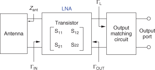
Figure 4.1 shows the functional blocks of an LNA, including its input- and output-matching circuits, at a typical receiver. Good stability, high gain, low noise, low power consumption, and low cost are among the important criteria of an LNA. To have unconditional stability, in amplifier design, it is crucial to bias a transistor so that the conditions stated in (4.1) and (4.2) are met. Condition (4.2) implies (4.3) and (4.4).
4.3 ![]()
4.4 ![]()
For an LNA, it is always very desirable to have a low noise factor F, which is defined as the ratio of the SNR at the input to the SNR at the output. The noise factor in decibels (10 log10F) is also called the noise figure (NF). Obviously, it is directly proportional to the noise that a transistor adds to the output signal. For a typical receiving active amplifying antenna, as shown in Fig. 4.2, the input-matching circuit is usually not needed. This can significantly reduce the footprint and circuit size.
Figure 4.1 Block diagram of a low-noise amplifier at a typical receiver.

Figure 4.2 Block diagram of a receiving active amplifying antenna.
4.3 Wearable Low-noise Amplifying Antenna
Configuration
In recent years, many passive wearable antennas have been reported (12–16). Research was also conducted to study the effects of the human body on such antennas (17, 18). In 2010, Declercq and Rogier (19) first proposed an active wearable antenna, made on garments. To demonstrate the design idea, an LNA is connected directly to a textile antenna without using an input-matching network. The impedance of the antenna is designed to match the input impedance of the LNA for optimal noise performance. In this case, the antenna impedance is designed to be coincident with the optimal impedance (of the transistor) for achieving a minimum noise figure. The schematic of the amplifier is shown in Fig. 4.3. It is designed using the biasing scheme recommended by Avago Technologies (20). With the use of the power dividing resistors R1 = 300 Ω, R2 = 1.2 kΩ, and R3 = 10 Ω, an Avago ATF-54143 + e-PHEMT transistor is biased in the common-source configuration with Vds = 3 V, Id = 60 mA, and Vgs = 0.56 V. A high-value resistor R4 = 10 kΩ has been used as the current limiter of the gate. Resistor R5 = 50 Ω functions as a resistive termination so that the low-frequency stability can be enhanced. The inductor L1 = 2.7 nH and the λ/4 high-impedance (100-Ω) microstrip are both RF chokes, while C3 is a dc block. The components C1 = C4 = 8.2 pF and C2 = 10, 000 pF are bypass capacitors, where C2 can further improve the low-frequency stability. An inductor L2 is for output matching, while R6 is for resistive loading. A flexible substrate made of a woven textile layer and a very thin flexible polyimid layer is used as a circuit board for accommodating the active devices and interconnects. The input port is connected directly to the receiving antenna through a via (diameter of 1 mm) to achieve low loss, low noise, and compact size.
Figure 4.3 Schematic of an LNA (19).
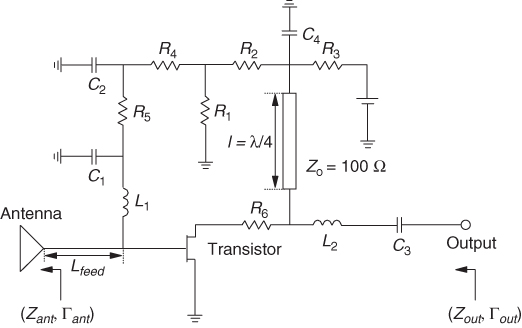
Figure 4.4 shows the configuration of the ring antenna being used. It is built on a double-layered substrate and is designed to cover the entire 2.4 to 2.484 GHz ISM band. The top layer is made of a flexible polyurethane foam with a thickness of h1 = 3.56 mm. As can be seen from the figure, the bottom layer consists of an aramid fabric (400 μm) and a polyimid textile (25 μm), together totaling to a substrate thickness of h2 = 425 μm. The antenna and ground are made from a type of copper-plated nylon fabric called Flectron. All the materials are glued together by adhesive. The properties of the materials are given in Table 4.1. An active wearable antenna that has a total area of 11 cm2 is shown in Fig. 4.5. As can be seen from the figure, the polyimid layer is kept as small as possible. Good bonding is formed between the aramid and polyimid layers.
Figure 4.4 Configuration of an active wearable antenna: (a) top view; (b) front view.

Figure 4.5 Active wearable antenna: (a) bottom view; (b) top view. (Courtesy of F. Declercq, Ghent University. From (19), copyright © 2010 IEEE, with permission.)
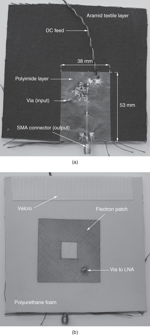
Table 4.1 Properties of the Materials for an Active Wearable Antenna

The co-design and co-optimization processes of the antenna and amplifier require both field- and SPICE-based CAD softwares. In this case, the commercial software Agilent ADS-Momentum and CST Microwave Studio are used jointly in designing the LNA and antenna, respectively. Material properties given in Table 4.1 have been used for all the simulations. To begin with, the LNA design is discussed. The transistor and all the lumped elements are simulated using Agilent's ADS. Momentum, a full-wave software affiliated with the ADS, can be employed for simulating the passive interconnects placed on the polyimid so that the parasitic effect can be accounted for. Then the antenna can be simulated using the field-based simulation software CST Microwave Studio, and the components can be combined using the following three-step co-design and co-optimization strategy (19):
As many solutions may meet the requirements, the simulated annealing was used as an optimization algorithm to find the global maximum. The co-optimized antenna and LNA parameters are shown in Tables 4.2 and 4.3. Also given in the tables are the design parameters for the isolated antenna and LNA. In general, the two groups of parameters are quite close to each other.
Source: (19).
Table 4.2 Design Parameters of an Isolated and Co-optimized Antenna
| Isolated Antenna | Co-optimized Antenna | |
| Lfeed | 3 mm | 4.73 mm |
| L1 | 7.7 nH | 10 nH |
| L2 | 2.6 nH | 1.2 nH |
Source: (19).
Table 4.3 Design Parameters (Millimeters) of an Isolated and Co-optimized LNA
| Isolated LNA | Co-optimized LNA | |
| L | 50.5 | 49.5 |
| W | 46.5 | 48 |
| xf | 15 | 15.5 |
| yf | 11 | 12 |
| lgap | 9 | 13 |
| wgap | 8 | 12 |
4.3.1.1 Results and Discussion
LNA Performance
The amplifier is first designed on the fabric materials without including the ring antenna. To measure the LNA output, the antenna is removed and the amplifier output is soldered to the center conductor of an SMA connector punching through the fabric. An Agilent N5242A PNA-X vector network analyzer (VNA) is used to measure the S parameters. The source-corrected noise measurement technique, which is a function affiliated to the PNA-X VNA, is adopted for measuring the noise figures (21). To account for the effects of the human body, the LNA is placed on a person's back for measurements. With reference to Fig. 4.6, the simulated and measured amplifier gains (|S21|) and noise figures are compared, with good agreement observed. The measured amplifier gain is 11.18 dB at 2.45 GHz, slightly lower than that for simulation (11.79 dB). As can be seen from the figure, the measured noise figure F = 1.25 dB is slightly higher than the simulated noise figure (0.87 dB). This on-body gain measurement shows that the active circuitry is not much affected by the human body despite it being directed toward the body without shielding. This is because the amplifier does not radiate and has little interaction with the human body. Figure 4.7 shows the simulated and measured stability factors K and B1. In general, good agreement is observed, with the LNA meeting all the conditions for unconditional stability (K>1 and B1 > 0).
Figure 4.6 Simulated and measured amplifier gain and noise figure for the LNA in Fig. 4.3. (Courtesy of F. Declercq, Ghent University. From (19), copyright © 2010 IEEE, with permission.)

Figure 4.7 Simulated and measured stability factors K and B1 for the LNA in Fig. 4.3. (Courtesy of F. Declercq, Ghent University. From (19), copyright © 2010 IEEE, with permission.)

Off-Body Active Antenna Performance
Amplifier Gain and Noise Figure Measurements of an Amplifying Antenna
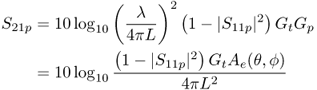
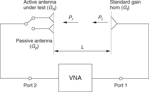
Now, the input port of the amplifier is connected to the optimized antenna. As the integrated antenna is now a one-port device, the conventional two-port method can no longer be used to measure the amplifier gain and noise figure. In 1994, An et al. (22) proposed a simple measurement method for receiving amplifying antennas. This method is adopted here. Figure 4.8 shows the configuration of a receiving active amplifying antenna. The transducer gain (GT) is defined as
4.5 ![]()
where Pav is the available power received by the antenna (with input impedance Zant) and PL is the power delivered to the load (with input impedance ZL). The total available gain (GA) of the active antenna can then be calculated:
4.6 ![]() Gp, the antenna gain of the passive antenna, can be defined as
Gp, the antenna gain of the passive antenna, can be defined as
4.7 ![]()
where Ae(θ, ϕ) is the effective aperture of the passive antenna.
Figure 4.8 Configuration of a receiving amplifying antenna.

The measurement is conducted inside an anechoic chamber, with the setup shown in Fig. 4.9. A transmitting standard gain horn is connected to port 1 of a VNA, and the receiving active amplifying antenna is connected to port 2. A similar passive antenna is also fabricated by removing the amplifier part. The distance (L) between the horn and the antenna under test must satisfy the far-field condition (L > 10λ and L > 2D2/λ), where D is the maximum dimension of the antenna and λ is the operating wavelength. The transmission coefficients of the passive and active antennas are then measured, along with the reflection coefficient of the passive antenna. The Friis transmission equation states that S21a transmitting from the horn to the active antenna can be expressed as
where Gt is the antenna gain of of the standard gain horn.
If the active antenna is replaced by the passive antenna,
where S11p is the reflection coefficient of the passive antenna. Subtracting (4.9) from (4.8), we obtain
4.10 ![]()
Therefore,
The transducer gain GT can easily be calculated from (4.11) by knowing the reflection and transmission coefficients of the active and passive antennas.
Figure 4.9 Measurement setup for amplifying antenna [22].
Next, the noise figure measurement is discussed. With the knowledge of GT, the noise factor of the receiving active amplifying antenna can be calculated using (4.12). The noise figure is defined as NF = log10F.
where Pn is the absolute power of noise density that can be measured directly by a noise figure meter, and Ta is the ambient room temperature.
Available Gain and Noise Figure
In the measurement setup (Fig. 4.9), an Agilent N5242A PNA-X vector network analyzer (VNA) was used to measure the transmission (S21a, S21p) and reflection (S11p) coefficients in an anechoic chamber. The absolute noise power density Pn was measured using the calibrated receiver of the PNA-X VNA. Measuring Pn at the output of the active antenna requires a long cable which has been included in the calibration. Inside the anechoic chamber, Ta is usually taken to be 300 K. The simulated and measured results are compared in Fig. 4.10, with good agreement. Using (4.6) and (4.11), the measured available gain GA of the receiving active amplifying antenna is about 12 dB in the ISM frequency band (2.4 to 2.484 GHz), with a ripple amplitude of 0.5 dB. The simulated and measured noise figures are also given in Fig. 4.10 in the frequency range 2 to 3 GHz. An NF of about 1.3 dB is measured in the ISM band.
Figure 4.10 Simulated and measured NF and GA of the active amplifying antenna in Fig. 4.5. (Courtesy of F. Declercq, Ghent University. From (19), copyright © 2010 IEEE, with permission.)

On-Body Active Antenna Performance
To further understand the effect of a human body on an antenna, an active antenna is placed inside a firefighter's jacket made of the same fabric materials. The antenna is placed at two positions (1 and 2) on the person's back (19). For comparison, a similar passive antenna is measured at the same positions. Measurements were conducted in an anechoic chamber using the experimental setup described in Fig. 4.9. The free space and on-body total gains Gtot (or the total available gain GA) of the active antenna were measured in the frequency range 2 to 3 GHz at both positions on the back, with the results shown in Fig. 4.11. Also depicted in the same figure are the antenna gains of the passive antenna at the two positions. The maximum free-space Gtot of the receiving amplifying antenna is about 17 dBi. As can be seen from the figure, human body has caused 1 to 3 dB of power loss to Gtot, depending on the position at which the antenna is placed on the body. It is also noted that the human body causes a noticeable degradation (about 1 to 3 dB) of the antenna gain. It is worth mentioning that position 1 has a higher loss because it is placed closer to the skin. Figure 4.12 shows the simulated and measured reflection coefficients in free space and on the body. As can be seen from the figure, the human body does not greatly affect the impedance matching. The discrepancy between the simulated and measured results can be caused by various experimental tolerances, which are quite significant in this case.
Figure 4.11 Measured gains of a receiving amplifying antenna at different body positions. (Courtesy of F. Declercq, Ghent University. From (19), copyright © 2010 IEEE, with permission.)

Figure 4.12 Simulated and measured reflection coefficients of the receiving amplifying antenna in Fig. 4.5 at various settings. (Courtesy of F. Declercq, Ghent University. From (19), copyright © 2010 IEEE, with permission.)

4.4 Active Broadband Low-Noise Amplifying Antenna
Configuration
In this section, the resistive equalization technique is used for co-designing and co-optimizing a broadband amplifying patch antenna. With the use of two equalizing resistors, the input impedance of a dual-band patch antenna can be configured to locate within the region where the field-effect transistor (FET) has the optimum noise figure. To demonstrate the design idea, a broadband receiving antenna is designed to cover the DCS-1800 and UMTS frequency bands.
Antenna Design
The double-layered patch antenna reported by Rajo-Iglesias et al. (24) will be adopted for designing the following amplifying antenna. Figure 4.13 shows the antenna configuration, along with the design parameters: W = 38 mm, h = 6 mm, d1 = 10 mm, h = 6 mm, and ε r = 3. It has a ground size of 260 × 260 mm2. Given in Fig. 4.14(a) is the measured input impedance of the passive antenna with d2 = 4 mm. As can be seen clearly from the figure, the antenna has two resonances, at 1.91 and 2.192 GHz. The antenna gain is about 7 ± 1.5 dB. Also shown on the same figure is the impedance region in which the FET has optimum noise (discussed in the next section). With reference to Fig. 4.14(a), unfortunately, the impedance locus of the antenna is far away from the optimum noise impedance region of the FET, which is very undesirable. It causes the amplifier to have a higher noise figure. By increasing the offset of the top–bottom patches to d2 = 9 mm, shown in Fig. 4.14(b), a small portion of the impedance locus (around the resonances) can be moved into the optimum region. It will later be shown in the co-design process that the use of equalizing resistors can squeeze even more of the impedance locus of the antenna into the optimum noise impedance region.
Figure 4.13 Double-layered wideband patch antenna (24).

Figure 4.14 Input impedance of the double-layered antenna in Fig. 4.13 with (a) d2 = 4 mm; (b) d2 = 9 mm. (Courtesy of D. Segovia-Vargas, Carlos III University. From (23), copyright © 2008 IEEE, with permission.)

Amplifier Design
The ATF34143 MESFET (Avagotech, San Jose, CA) is deployed for designing a low-noise amplifier. At a dc bias of Vds = 3 V and Ids = 20 mA (25), the transistor has a minimum noise figure of Fmin = 0.17 dB at 1.8 GHz, with the input port optimized to have Γs = Γopt = 074∠57°. When applying the resistive equalization technique, the antenna is made to provide this impedance Γant = Γopt. The small-signal model (inside the dashed square) of the FET is shown in Fig. 4.15, along with all the parasitics. As can be seen from the figure, gm is the transconductance of the transistor. Rg = Rgate and Rd = Rdrain are the external resistors that will be used for resistive equalization later.
Figure 4.15 Equivalent circuit of an FET at low frequencies. (Courtesy of D. Segovia-Vargas, Carlos III University. From (23), copyright © 2008 IEEE, with permission.)

Co-design of the Active Broadband Receiving Antenna
By connecting the antenna to the gate of the FET, a broadband amplifying antenna can be designed for the receiver, as shown in Fig. 4.16. The biasing voltages and current of the FET are Vds = 3 V, Vgs = − 0.5 V, and Ids = 20 mA. The prototype (circuit side) is shown in Fig. 4.17. The antenna is built on the opposite side (not shown). It is obvious that no input-matching network is used for this active circuit. With reference to the figure, two resistors, Rg and Rd, have been added to the amplifier to optimize the antenna efficiency and noise figure. Now, the resistive equalization technique is applied to meet the following design criteria:
Figure 4.16 Configuration of a broadband amplifying antenna. (Courtesy of D. Segovia-Vargas, Carlos III University. From (23), copyright © 2008 IEEE, with permission.)

Figure 4.17 Broadband amplifying antenna. (Courtesy of D. Segovia-Vargas, Carlos III University. From (23), copyright © 2008 IEEE, with permission.)

As the input impedance of the antenna is complex and far from the resonance conditions, the generalized S parameters (26, 27) can be used to analyze the network, shown in Fig. 4.18. Assuming that the input and output ports of the amplifier are ports 1 and 2, respectively, the matching condition at port 1 (Zant = Zin*) implies that
4.13 ![]()
where [S] denotes the S-parameter matrix of the FET.
Figure 4.18 Generalized S parameters for a broadband amplifying antenna. (Courtesy of D. Segovia-Vargas, Carlos III University. From (23), copyright © 2008 IEEE, with permission.)

By assuming that ZL = Z0 and ΓL = 0 (Z0 is the reference characteristic impedance), the generalized S parameters of the network in Fig. 4.18 can be written as
4.14 ![]()
Conditions (4.13) and (4.14) imply that ![]() . Also, it is equal to the optimum noise impedance of the transistor, Γant = Γopt. Considering the lossy small-signal model in Fig. 4.15, the inclusion of lossy shunt elements to the gate (Ygate) and drain (Ydrain) of the FET leads to the new S11 expression.
. Also, it is equal to the optimum noise impedance of the transistor, Γant = Γopt. Considering the lossy small-signal model in Fig. 4.15, the inclusion of lossy shunt elements to the gate (Ygate) and drain (Ydrain) of the FET leads to the new S11 expression.
4.15 ![]()
where Yij are the Y parameters of the FET. For the common case Gdrain|Y21|2Rn, the minimum noise figure is given by
4.16 
where Rn is the resistance of the equivalent noise voltage generator and Gcorr is the correlated admittance between the voltage and current noise generators. The total noise figure can then be expressed as
4.17 ![]()
where Gopt and Bopt are defined as
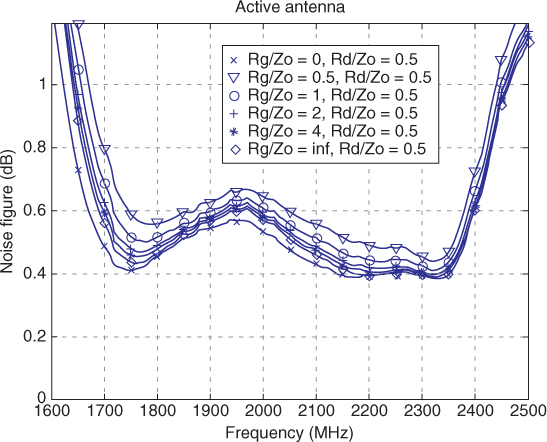
It can be seen from eq. (4.18) that the noise figure is affected by the gate conductance. The effect of gate conductance is studied in Fig. 4.19. As can be seen from the figure, a higher Rg/Z0 value is good for a lower noise figure.
Figure 4.19 Effect of the gate conductance on Ftotal across the frequency. (Courtesy of D. Segovia-Vargas, Carlos III University. From (23), copyright © 2008 IEEE, with permission.)
Using the model in Fig. 4.18, the transducer gain (GT) can be defined as
4.19 ![]()
4.20 ![]()
where the transmission coefficient S21 is defined as
4.21 ![]()
4.4.1.2 Results and Discussion
The AWR Microwave Office was used to optimize the models in Figs. 4.15 and 4.16, and it was found that the optimized drain and gate resistances are Rd = Rdrain = 91 Ω and Rg = Rgate = 68 Ω, respectively. With reference to Fig. 4.16, two high-impedance lines (Z0 = 90 Ω, with an electrical length of 90°) are used to compensate the effect of losses at higher frequencies. The new input impedance of the antenna (inclusive of Rd and Rg) is shown in Fig. 4.20. The addition of the two resistors causes the locus of the antenna impedance to become narrower. Therefore, a larger portion of the locus can then be squeezed into the region in which the FET has optimum noise. Also plotted on the figure is the locus of the optimum noise impedance of the FET. It can be seen from the figure that better impedance matching can now be obtained as the two loci are closer to each other [compared to Fig. 4.14(b)]. These two resistors are called equalizing resistors.
Figure 4.20 New input impedance of a double-layered patch antenna (with inclusion of Rd and Rg). Also given is the locus of the optimum noise impedance of the FET. Z. Trans refers to the optimum noise impedance of the transistor and Z. Patch refers to the new input impedance of the antenna. (Courtesy of D. Segovia-Vargas, Carlos III University. From (23), copyright © 2008 IEEE, with permission.)

Now, the gain of the active antenna is characterized. For an active amplifying antenna, its effective transmission gain (GTX) can be obtained by comparing its transmission coefficient to that of its passive counterpart. Of course, GTX is a figure that combines the antenna and amplifier gains. A standard reference horn is used for measurement in an anechoic chamber. With reference to Fig. 4.21, the measured GTX( = ΔS21) reads about 13 dB across the frequency passband. It is then compared with the simulated GT of the isolated amplifier in Fig. 4.22. It is worth mentioning that the antenna impedance is used as the port impedance at the input. As can be seen from the figure, the simulated GT agrees reasonably well with the measured GTX.
Figure 4.21 Measured effective transmission gain (GTX) of active and passive antennas. (Courtesy of D. Segovia-Vargas, Carlos III University. From (23), copyright © 2008 IEEE, with permission.)
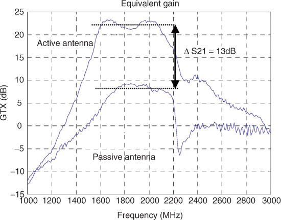
Figure 4.22 Comparison of the simulated transducer gain (GT) and the measured effective transmission gain (GTX). (Courtesy of D. Segovia-Vargas, Carlos III University. From (23), copyright © 2008 IEEE, with permission.)

The ratio of antenna gain to effective system temperature (G/T) ratio is a figure of merit that describes the performance of an AIA (28, 29). For an active antenna, its G and T cannot be measured separately. The G/T ratio is defined as
4.22 ![]()
with the following parameters:
| GACT | antenna gain of the active antenna |
| ΔG | total gain, including antenna gain, amplifier gain, and losses |
| Le | loss factor (>1) |
| L | losses |
| T0 | physical temperature of the antenna |
| Ta | temperature of the active antenna |
| Tre | receiver equivalent noise temperature |
Once G/T is known, the total noise figure of the active antenna can be calculated:
Figure 4.23(a) shows the measurement setup for the active antenna in an anechoic chamber. With reference to the figure, a section of 50-Ω transmission line (with a loss of 2 dB) is used to connect the active antenna to the receiver (with a loss of 8 dB). The passive antenna can be measured by the setup in Fig. 4.23(b). In this case, the antenna is connected to an external LNA through a section of transmission line (with a loss of 2 dB). Figure 4.24 shows the measured G/T of the active antenna for different (Vds, Vgs) biasing conditions. Several combinations (1.5V, 0.5V), (2.5V, 0.5V), (3.0V, 0.6V), and (3.5V, 0.6V) were tested. Also shown on the figure is the measured G/T of the passive antenna. When biased at Vds = 2.5 V and Vgs = 0.5 V, the ratio G/T is about −16 dB/K in the frequency range 1.5 to 2.05 GHz (bandwidth of ∼30%), as can be seen from Fig. 4.24. It is 4 to 6 dB better than that for the passive antenna.
Figure 4.23 Measurement setups for (a) an active antenna; (b) a passive antenna. (Courtesy of D. Segovia-Vargas, Carlos III University. From (23), copyright © 2008 IEEE, with permission.)
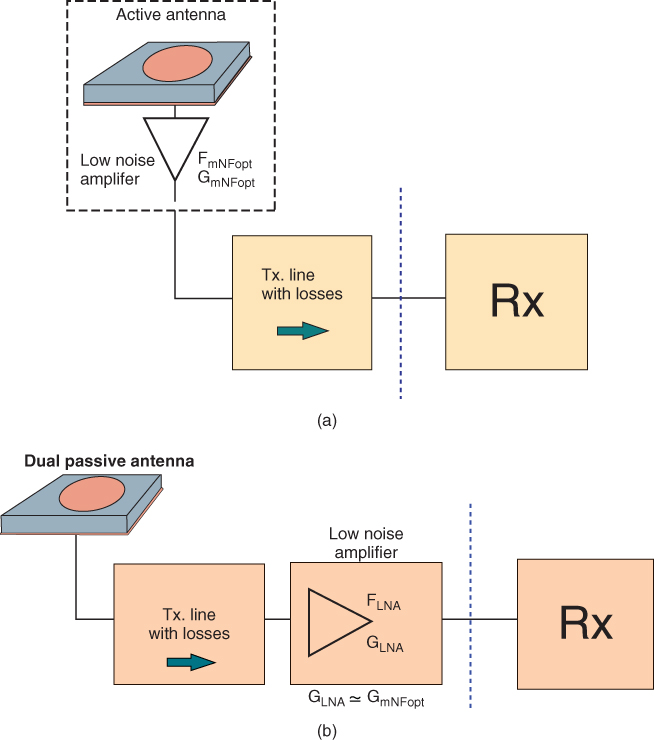
Figure 4.24 Measured G/T of the active antenna in Fig. 4.16 with different biasing conditions (Vds and Vgs). Also shown is the measured G/T of a passive antenna. (Courtesy of D. Segovia-Vargas, Carlos III University. From (23), copyright © 2008 IEEE, with permission.)

By letting the antenna temperature T0 = Ta = 290 K and knowing the G/T ratio, the noise figure NF can be calculated using (4.23). Figure 4.25 shows the NF calculated from the simulated and measured G/T values. With reference to the figure, the NF measured at 1.8 GHz is about 0.5 dB, being higher than that given in the datasheet (0.17 dB).
Figure 4.25 Comparison of noise figures (NFs) calculated from simulated and measured G/T. (Courtesy of D. Segovia-Vargas, Carlos III University. From (23), copyright © 2008 IEEE, with permission.)

Figure 4.26 shows the simulated and measured reflection coefficients of the broadband amplifying antenna. Since port 1 of the amplifier is now connected to the antenna, the S22 notation is used to denote the reflection coefficient at the new input port of the active antenna. Three resonances are observed in both the simulation and measurement, with reasonable agreement. Also shown in the figure is the measured reflection coefficient of the passive antenna. It is higher because the antenna works in the nonresonant modes. Figure 4.27 shows the radiation patterns measured for the active and passive antennas at 1.8 and 2.2 GHz, both in the E-plane. They have almost the same field patterns, implying that the amplifier does not greatly disturb the far-field characteristics of the passive antenna.
Figure 4.26 Simulated and measured reflection coefficients (S22) of the active antenna in Fig. 4.16. Also shown is the S22 measured for a passive antenna. (Courtesy of D. Segovia-Vargas, Carlos III University. From (23), copyright © 2008 IEEE, with permission.)

Figure 4.27 Co-polarized fields measured for active (solid line) and passive (dashed line) antennas in the E-plane. (Courtesy of D. Segovia-Vargas, Carlos III University. From (23), copyright © 2008 IEEE, with permission.)

4.5 Conclusions
In this chapter, the co-design and co-optimization processes of receiving amplifying antennas have been explored. In the first part, the amplifying antenna is made on textile and is wearable. The interaction between an antenna, an LNA, and the human body has been studied. It has been found in the second part that wide impedance matching is achievable by deploying two equalization resistors to the gate and drain of a FET. For both parts, the antenna performance is not greatly affected by the amplifier.
References
1. A. D. Frost, Parametric amplifier antenna, Proc. IRE, vol. 48, pp. 1163–1164, June 1960.
2. A. D. Frost, Parametric amplifier antenna, IEEE Trans. Antennas Propag., vol. 12, no. 2, pp. 234–235, Mar. 1964.
3. J. R. Copeland, W. J. Robertson, and R. G. Verstraete, Antennafier arrays, IEEE Trans. Antennas Propag., vol. 12, no. 2, pp. 227–233, Mar. 1964.
4. V. Radisic, S. T. Chew, Y. X. Qian, and T. Itoh, High-efficiency power amplifier integrated with antenna, IEEE Microwave Guided Wave Lett., vol. 7, pp. 39–41, Feb. 1997.
5. W. R. Deal, V. Radisic, Y. X. Qian, and T. Itoh, Novel push–pull integrated antenna transmitter front-end, IEEE Microwave Guided Wave Lett., vol. 8, no. 11, pp. 405–407, Nov. 1998.
6. M. J. Cryan, P. S. Hall, S. H. Tsang, and J. Sha, Integrated active antenna with full duplex operation, IEEE Trans. Microwave Theory Tech., vol. 45, pp. 1742–1748, Oct. 1997.
7. Y. Chung, S. S. Jeon, S. Kim, D. Ahn, J. I. Choi, and T. Itoh, Multifunctional microstrip transmission lines integrated with defected ground structure for RF front-end application, IEEE Trans. Microwave Theory Tech., vol. 52, pp. 1425–1432, May 2004.
8. J. A. Navarro and K. Chang, Integrated Active Antennas and Spatial Power Combining. New York: Wiley, 1996.
9. A. Mortazawi, T. Itoh, and J. Harvey, Active Antennas and Quasi-optical Arrays. Piscataway, NJ: IEEE Press, 1998.
10. R. A. York and Z. Popovic, Eds., Active and Quasi-optical Arrays for Solid-State Power Combining. New York: Wiley, 1997.
11. M. P. Delisio and R. A. York, Quasi-optical and spatial power combining, IEEE Trans. Microwave Theory Tech., vol. 50, pp. 929–936, Mar. 2002.
12. P. O. Salonen, Y. Rahmat-Samii, H. Hurme, and M. Kivikoski, Dualband wearable textile antenna, Proceedings of the IEEE Antennas and Propagation International Symposiun, vol. 1, pp. 463–467, 2004.
13. A. Tronquo, H. Rogier, C. Hertleer, and L. Van Langenhove, Robust planar textile antenna for wireless body LANs operating in 2.45GHz ISM band, Electron. Lett., vol. 42, no. 3, pp. 142–143, Feb. 2006.
14. I. Locher, M. Klemm, T. Kirstein, and G. Tröster, Design and characterization of purely textile patch antennas, IEEE Trans. Adv. Packag., vol. 29, pp. 777–788, Nov. 2006.
15. T. F. Kennedy, P. W. Fink, A. W. Chu, and G. F. Studor, “Potential space applications for body-centric wireless and e-textile antennas,” Proceedings of the IET Seminar on Antennas, Propagstion and Body-Centric Wireless Communications, pp. 77–83, Apr. 2007.
16. C. Hertleer, H. Rogier, L. Vallozzi, and L. Van Langenhove, A textile antenna for off-body communication integrated into protective clothing for fire-fighters, IEEE Trans. Antennas Propag., vol. 57, pp. 919–925, Apr. 2009.
17. P. S. Hall, Y. Hao, Y. I. Nechayev, A. Alomainy, C. C. Constantinou, C. Parini, M. R. Kamarudin, T. Z. Salim, D. T. M. Hee, R. Dubrovka, A. S. Owadally, W. Song, A. Serra, P. Nepa, M. Gallo, and M. Bozzetti, Antennas and propagation for on-body communication systems, IEEE Antennas Propag. Mag., vol. 49, no. 3, pp. 41–58, June 2007.
18. G. A. Conway and W. G. Scanlon, Antennas for over-body-surface communication at 2.45GHz, IEEE Trans. Antennas Propag., vol. 57, pp. 844–855, Apr. 2009.
19. F. Declercq and H. Rogier, Active integrated wearable textile antenna with optimized noise characteristics, IEEE Trans. Antennas Propag., vol. 58, pp. 3050–3054, Sept. 2010.
20. ATF-54143: High Intercept Low Noise Amplifier for the 1850–1910MHz PCS Band Using the Enhancement Mode PHEMT. Application Note 1222, Avago Technologies, 2006.
21. K. Wong, Advancements in Noise Measurement. http://www.ewh.ieee.org/r6/scv/ims/archives/May2008Wong.pdf
22. H. An, B. K. J. C. Nauwelaers, A. R. Van de Capelle, and R. G. Bosisio, A novel measurement technique for amplifier-type active antennas, IEEE MTT-S International Symposium Digest, vol. 3, pp. 1473–1476, 1994.
23. D. Segovia-Vargas, D. Castro-Galán, L. E. García-Mu noz, and V. González-Posadas, Broadband active receiving patch with resistive equalization, IEEE Trans. Microwave Theory Tech., vol. 56, pp. 56–64, Jan. 2008.
24. E. Rajo-Iglesias, D. Segovia-Vargas, J. L. Vázquez-Roy, V. González-Posadas, and C. Martín-Pascual, Bandwidth enhancement in noncentered stacked patches, Microwave Opt. Tech. Lett., vol. 31, no. 1, pp. 32–34, Oct. 2001.
25. ATF-34143: Low Noise Pseudomorphic HEMT in a Surface Mount Plastic Package. Avago Technologies, 2009.
26. R. Collin, Foundations for Microwave Engineering, 2nd ed. New York: McGraw-Hill, 1992.
27. K. Kurokawa, Power wave and the scattering matrix, IEEE Trans. Microwave Theory Tech., vol. 13, pp. 194–202, Mar. 1965.
28. J. J. Lee, G/T and noise figure of active array antennas, IEEE Trans. Antennas Propag., vol. 41, pp. 241–244, Feb. 1993.
29. U. R. Kraft, Gain and G/T of multielement receive antennas with active beamforming networks, IEEE Trans. Antennas Propag., vol. 48, pp. 1818–1829, Dec. 2000.