
Hardware Debug*
Matt saw Cody hunched over a bench as he strolled through the lab. As he approached, he could see a printed circuit board, populated with components, and an oscilloscope on the bench beside it. “How’s it going?” he asked.
“It’s not,” Cody said. “It looks dead. The processor doesn’t even run.”
“What code have you got in the EPROM?”
“Do you have special test code, or your application code?”
Matt frowned. “How are you going to tell if your problems are hardware or software?” he asked. “You’ve got unknown software running, or apparently, not running, on untested hardware.”
“How about testing the hardware in small chunks, then working on your software when you’ve got some level of confidence in the hardware?”
Cody reached over and switched off the power supply that was connected to his board. “Okay,” he said. “A divide-and-conquer strategy. I’m listening.”
Matt picked up a pad of paper from the bench and handed it to Cody. “List the functional blocks from your block diagram,” he said.
Cody thought a moment, then scribbled the following list:
Programmer Hordwom Components
80188 Microprocessor
16550 UART/RS-232 interface
PIO chip (8255)
Control register
RAM memory
ROM memory
Vpp and Vcc DAC
“You will probably want to test this from the bottom up,” Matt said. “Start with the processor and associated components, then test the memory because you’ll need that for more sophisticated tests. Then verify the UART so you can use your host computer for debugging if you want, then, finally, the PIO, DACs, and control register that control your target EPROM. If you had an emulator, you could do some of this directly through it, but we’ll have to do this the hard way. Come back to my office. I think I’ve got some code fragments from an earlier project that you can use.”
Matt took the same vinyl binder from his bookcase and thumbed through it. “Here’s a simple code fragment that just sets up the 80188 internal registers and then hangs in a tight loop. It will let you check out basic EPROM and RAM addressing, and let you make sure you’ve got the basic 80188 setup right.” He turned the page around so Cody could read it.
“Just a ’scope. If everything works, you’ll see periodic low-going pulses on the diagnostic output (Pin 7 of the 74AC138) and on the RAM chip select signal. That will tell you that you’ve got the internal chip-select and other registers set up correctly.”
Cody nodded. “This shouldn’t take long,” he said.
An hour later, Matt found Cody scratching his head over the prototype board. “Still dead?” Matt asked.
“Yes. I can’t get it to do anything.”
“Is the processor clock running?”
In answer, Cody touched the ’scope probe to the CLKOUT signal from the processor where it connected to the UART at pin 16. A clean square wave appeared on the screen.
“Have you checked the supply voltage?” Matt asked.
“Hmm.” Matt opened the toolbox he was carrying and pulled out a logic probe. “Connect this to the processor READ line,” he said.
Cody studied the schematic for a moment, then used a short clip-lead to connect the logic probe to pin 21 of the UART IC. The logic probe LED remained dark. Matt picked up the board and flexed it, looking for intermittent runs, then ran his fingers over the back, and the LED flickered. “You’ve got a floating pin somewhere,” he said. “All your parts are CMOS, and the skin resistance of my fingers is driving something to a valid state.”
Cody studied the board. “Here it is,” he said. “The reset resistor and capacitor weren’t installed. I remember we didn’t have the parts, so we ordered some and the tech said he’d put them in later. He probably forgot.” Cody went to the parts drawers and selected components, then soldered them into the circuit. Now when he turned on the power supply, the logic probe LED blinked once and went out. “That’s better,” Cody said. “At least it does something.”
Matt reached into his toolbox once again. “I thought we might need this, so I took it out of the cabinet this morning.” He handed a handwired perfboard to Cody.
“It’s a circuit that will let us single-step the processor. You brought one of the RDY lines out to a test point, right?”
“Just like you said,” Cody replied. He studied the schematic for a moment, then clipped the four wires from the perfboard into the circuit. “How does it work?”
Matt pulled a paper from his toolbox and unfolded it. “A copy for you,” he said (see Figure 4.1).
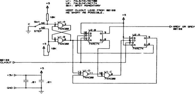
“You probably recognize the momentary switch and the two 74AC00 gates as a set-reset flip-flop wired to debounce the switch,” Matt said. “The rest of the circuit drives the RDY pin high for two clocks each time the pushbutton is pressed.”
“Turn your circuit on. The stepper circuit will hold the processor in a wait state so you can look at the EPROM address and data lines to see what the data is. If the first byte from the EPROM is wrong, nothing else is going to work either.”
Cody nodded and turned on the power supply, then checked each EPROM pin with the logic analyzer. He looked at this code listing. “The first byte is right,” he said. He pushed the button several times, checking the data lines each time. “The data is all 1s here,” he finally said.
Cody busied himself for a moment. “Got it. The address isn’t what I expected. It’s at a place where there’s no code. I bet I’ve got a problem with the way I linked the reset code in. It’s probably generating a jump to the wrong place. Let me look at this and get back to you if I still have problems.”
“Will do. Oh, and I was talking to Josh about the design. He thinks I need to be able to change the baud rate, instead of fixing it at 9600. I’d like to talk that over with you later.”
Tests
Let’s take a look at Cody’s test log when he ran the rest of the tests:
Test 1 (init test). Verified that strobe and RAM CS are toggling. Verified positive and negative RS-232 charge pump voltages.
Test 2 (RAM test). Allowed test to run for 2 hours. No failures.
TxTEST1. Transmits character “A” continuously. Used ’scope to verify bit time at 104 microseconds (9600 baud). Connected to PC, started communications program, verified that continuous characters are seen by PC.
TxTEST2 (wraparound test). Connected Tx to Rx, allowed test to run 30 minutes. No errors.
PIO TEST. Verified that frequency of each succeeding pin halves.
DAC TEST. Used DSO to verify that both DACs produce sawtooth voltage.
The tests chosen for this system are typical of what you might see when debugging the hardware for a new design. Each of the test routines and the expected results are described below:
The first listing in Appendix 1 is a basic test to verify that the code sets up the 80188 internal registers correctly. The 80188 is a high integration device and can generate chip selects for the PROM, RAM, and I/O internally. These must be set up correctly before the processor can even get instructions from memory. Other processors will not have the same configuration, but may have other internal or external peripherals that must be initialized. When the code is running correctly, the 80188 will produce a regular pulse on the diagnostic output strobe (74AC138 pin 7), and a regular pulse pair on the RAM CE pin. These can be observed with a ’scope. The test also sets up the UART for 9600 baud operation, so the baud clock output can be verified as well.
The second code fragment is a RAM test, to verify the 128k SRAM. The test holds all variables in 80188 registers, so it does not need a functional RAM to run. In operation, the test writes location 0 with 0, location 2 with data 1, and so on, until the RAM is full. (The address increments by two because the code uses word writes.) After the data is written, it is verified. Then the initial value is incremented by 1 and the test runs again. If the test runs long enough, every location will be tested with every possible value. The test also toggles the bipolar LED between red and green for each read/write pass.
When running, a ’scope will reveal pulse pairs on the processor WR line (paired because of the word writes). These will appear for a few seconds, then they will go away while the data is verified. If there are no errors, the pulses will reappear every few seconds as a new set of data values are written to the RAM. If we were using an 80186 in our example, which has a 16-bit data bus, the write pulses would not be paired because only one write cycle would be needed for a word write.
Before testing the serial interface, the test log shows that the RS-232 voltages were verified. The MAX232 family of parts uses a charge pump to generate the positive and negative voltages needed to drive the RS-232 line. If the chip is not working (or is wired wrong), these voltages will not be present and the RS-232 lines will not work.
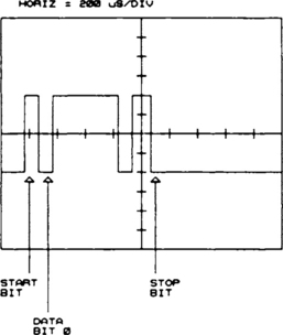
The first transmit test, TxTEST1, just continuously sends the character “A” to the serial port. This sort of test lets us check the bit timing with a ’scope and allows us to verify the slew rate of the signal. Figure 4.2 shows the waveform of one character as seen on a ’scope connected to the RS-232 transmit line while running this test. Note that the waveform is inverted (a high is the lowest voltage) with respect to the logic level prior to the RS-232 buffer. The waveform in the figure shows a single character for clarity; the actual code transmits the character continuously.
TxTEST2, the second serial test, sends a byte to the transmit half of the UART, then waits for the byte to be received and verifies it against the transmitted data. The transmitted byte is then incremented and the process repeats, continuously sending all 256 possible 8-bit values. The bicolor LED alternates between green and red while the test is running, producing an amber color. If a transmitted byte is never received, the LED stays green, and a byte that does not verify leaves the LED red and stops the test. To execute the test, the Tx and Rx lines must be shorted together with a jumper wire (pins 2 and 3 of the DB-9 connector).
PIOTEST continuously increments a 16-bit value and writes it to ports A and B (A is the LS byte). Using a ’scope to view each port output, and working from Port A bit 0 toward Port B bit 15, each pin in turn will display a waveform with a frequency that is half that of the previous pin. This permits a single test to be used to verify PIO operation and correct connection to the PROM programming connector.
DACTEST, the last test listed, writes incrementing values to both DACs. Since the value wraps from 255 to 0, the resulting waveform is a slow sawtooth (Figure 4.3). If the ’scope sweep speed is set slow enough, the individual steps will be visible as shown in the magnified section (they won’t look that clean and noise-free, of course!).

These tests are unique to this circuit, of course, but they indicate the sort of thing that can be accomplished with limited equipment and some simple software.
The more powerful your tools, the simpler this process can be. If you are using an emulator or software debugger, for example, the UART registers can be set up manually by directly writing to the register addresses and verifying that the baud clock is correct, the test character is correctly sent and received, and so on. One advantage to actually writing test code, however, is that the initialization code, once debugged, may be useful directly in the application code.
Hardware Problems and Solutions
Now that we’ve looked at the programmer to see a typical example of the hardware debug process, we’ll take a look at some common hardware problems and how to go about solving them.
Floating Pins
Many years ago, an engineer came looking for suggestions about a problem he was having. He had a microprocessor circuit, with a UV-erasable EPROM, and the circuit would work only when he opened the cover of the box it was installed in, or if he put a flashlight in the box with the cover closed. It turned out the Vpp pin (where the programming voltage is applied during programming) was floating. Apparently, the chip needed just a little light (through the erasure window, which wasn’t covered) to bias everything up so it would work.
In the days when everything was TTL, a floating input would show up on a ’scope as about 1 to 2 volts. Now that nearly everything is CMOS, floating inputs usually look like ground. Often, if you run your fingers over the board, circuit operation will change. Also, if you have an IC, such as an 8-bit register, that fails only with certain data patterns, look for a missing ground. Many CMOS parts will work without a ground connection as long as one of the inputs is low, but as soon as they all go high, everything stops.
It is often safe to leave unconnected, unused pins floating on a microprocessor, but I like to pull them to an inactive state, in case they are needed. Microcontrollers with internal pull-ups, of course, need no other termination in most cases.
Risetime Problems
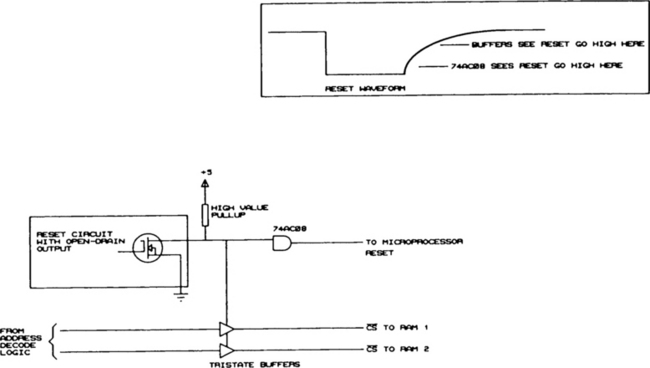
I worked on a problem once with a circuit that would fail powerup reset intermittently, and then only on some boards. Figure 4.4 shows what was happening. Apparently to save power, the designer had used large-value pull-ups (>100k). The RAM was backed up by a battery, and the tristate buffers prevented inadvertent writes to the RAM chips during the unstable interval while power was coming up. The problem was that the 74AC08 inputs on some of the boards saw the reset go inactive before the tristate buffer did. The result was that the processor would come out of reset before the RAM circuit was ready, so it couldn’t access the RAMs. Instant crash.
In another instance, a designer had used a 68000-family part with a pull-up that was too large, making the risetime of a signal longer than the specification allowed on the microprocessor data sheet. The circuit worked in production for several months, and then purchasing bought a different brand of processor chips, which was less forgiving of the input transition time.
Peripheral Timing Problems
Look at the diagram in Figure 4.5, which shows the timing cycle for a microprocessor accessing a peripheral IC. There are six timing parameters shown here, any of which can cause problems.
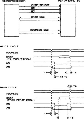
Figure 4.5 shows the typical timing for an Intel-style processor communicating with some generic peripheral IC. The chip select may come from an address decoder internal to the microprocessor itself, or from external address decode logic.
In the write cycle, the processor asserts the address, then asserts the –WR signal, then presents data to the peripheral. Time T1 on the diagram is the address setup time prior to –WR going low. If this parameter is not met, the wrong register (or memory location) inside the peripheral IC may be changed. Time T2 is the hold time of the data after the rising edge of –WR. If this is not met, the peripheral may store the wrong data. The last parameter, T3, is the minimum length of the –WR pulse itself. Some peripherals have a maximum parameter as well.
In the read cycle, time T4 is the address setup time prior to the falling edge of –RD. Not meeting this parameter is usually less critical than the equivalent parameter in the write cycle, unless the peripheral latches the address on the falling edge of –RD. Time T5 is the time the data must be stable prior to the rising edge of –RD and is effectively the access time of the peripheral IC. If it is not met, the processor may read the wrong data. Time T6 is the hold time of the data after the read cycle is complete. This is more likely to be a problem on a processor with a multiplexed address/data bus, where a peripheral that does not release the bus quickly enough can cause bus contention on the next cycle.
These parameters are typical of what you see in processor/peripheral data sheets. There are others, of course. Some peripherals have a parameter on the minimum time between successive accesses or require that input signals be synchronized to a clock. Sometimes they want write data to be stable before the leading edge of –WR, which requires additional logic on Intel-type processors. Other processors, such as the Motorola 68000 family, have different cycle and signal structures, but the same types of timing requirements apply.
Many designers just connect peripherals together, assuming that if the clock rates or the access times are right, everything else will work too. This can be dangerous, especially if production will run for many months or years, giving plenty of opportunity for parts from different manufacturing lots to be installed. Finding a timing problem is best done when the design is started, since fixing one can add a significant amount of logic to the board. You should verify that all timing parameters are met.
Rise time problems, timing problems, and floating-pin problems will often be temperature sensitive, showing up only when hot or cold. This is because the thresholds and speeds of the parts shift slightly with temperature. If you have an intermittent problem that you suspect is caused by one of these conditions, you can often make it show up by using circuit cooling spray or a hair drier to cool or heat the board. Be careful you don’t get it so cold the plastic IC packages crack, or so hot the packages melt.
EMI Problems
Embedded systems often must control stepper motors, DC motors, or relays. All of these can cause electromagnetic interference (EMI) problems. Any inductive device will cause EMI when it is switched on and off. Whether the EMI causes problems is another matter.
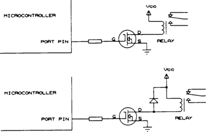
Figure 4.6 shows a microcontroller driving a relay through a port pin and a MOSFET transistor. In the top diagram, there is no protection diode between the transistor drain and the supply. When the port pin goes low, the MOSFET will turn off, opening the relay. However, the energy stored in the relay has to go somewhere; the result is a massive voltage spike on the drain of the transistor. Depending on the characteristics of the relay coil and the transistor, this flyback voltage can approach 100v—enough to destroy the transistor. The solution, shown in the lower diagram, is to add a snubber diode across the relay coil. The transistor drain is now clamped to one diode drop above the positive supply. For faster opening of the relay, a transient suppresser diode can be used instead, allowing the drain voltage to rise to some voltage between the supply and total destruction. If using a transient suppresser, remember that the drain voltage will rise to the sum of the supply voltage and the transient suppresser clamp voltage.
The catch, which is often overlooked, is that this fix is not really free. Adding a diode protects the transistor, but the coil energy still has to go somewhere, and it does. It takes the form of a current spike into the positive supply. If the supply is poorly bypassed, the result may be a voltage spike on the supply itself. When driving relays (or DC motors, or solenoids), take a little extra care to be sure the supply has adequate bypassing and that the path between the relay and the supply has a low impedance.
Figure 4.7 shows a microprocessor-based board driving a motor. For our purposes, the motor could be a DC motor, a stepper, or almost anything. When the motor is turned on, there will be a current increase, which passes through the ground wires back to the power supply and to chassis. The current causes a voltage drop, as indicated in the figure, because the wiring impedance (inductance plus resistance) is never zero. If the wiring inductance is high enough, the ground on the processor board can be upset far enough to affect operation or to corrupt communication with other boards in the system. This can be a particular problem with stepper motors or with DC motors that are PWM (pulse-width modulation) controlled, since there is usually a high-frequency surge every time the current is turned on.
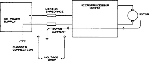
Figure 4.8 shows a way to minimize this problem. A third ground wire, not connected to logic ground, has been added to the system, and returns motor current to the power supply. The motor still causes a current surge, but it does not affect the logic ground. This solves the EMI problem, but it can cause other problems: the motor is usually driven from an H-bridge or other driver, and if the motor return and logic ground get too far apart, the H-bridge may be damaged.

Ground Loops
The classic case of a ground loop is two circuits that are connected to different grounds, and to each other, but the grounds have slightly different AC or DC potentials. Since the impedance between the two grounds is very low, significant current can flow in the grounds themselves.
Figure 4.9 shows an embedded microprocessor system communicating with a host PC. Both are powered by the 115v AC line. If the two systems are connected to different branches of the AC circuit (say, if they are in different rooms or different buildings), there can be significant current flowing in the ground. This current flows through the ground wires in the interface connections.

The problem of ground loop can be particularly bad if the two systems operate on different AC voltages. For example, if the microprocessor system is part of a large machine that requires 208V 3-phase power, real problems can occur. I have seen RS-422 drivers literally destroyed when the ground of an embedded system got yanked around by air conditioning compressors (which shared the 3-phase power) going on and off.
If the interface between our host PC and embedded system is RS-232 or serial RS-422, the problem can sometimes be solved by running the interface through an optical isolator pair. If the interface is parallel, a LAN, or some other high-speed interface, it may be necessary to ensure that the two systems are on the same branch of the AC line. In the case where the voltages are different, you may have to be sure that they both have clean, independent returns to the building ground, with no heavy-duty equipment sharing the ground return.
This same problem can occur within an embedded system that is composed of many boards and modules, each of which has a separate power supply. Sometimes you can fix these problems with a ferrite bead on the right cable, but that tends not to be a very permanent or repeatable fix.
Low-Level Signals
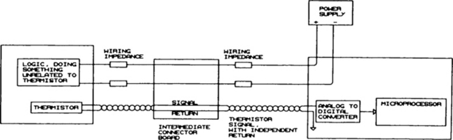
Ground loops do not have to affect the processor directly. They can instead affect the devices to which the processor connects. Figure 4.10 shows a processor board using a thermistor to read temperature. The thermistor has a fairly low output level—say, 1 mV per degree. The logic on the board where the thermistor is draws current, which causes voltage drops across the power supply wiring and all the connectors. The normal voltage drop typical of such systems is not enough to upset the logic, but it can be sufficient to cause an offset in the thermistor reading. Worse, the value may change as the DC current changes with the state of the logic. The solution to this problem (which was used in a similar real-world situation) was to give the thermistor a separate return so it was not affected by the offset voltage (see Figure 4.11). Of course, the same principle applies to strain gauges, pressure transducers, or any other low-level analog input device.

Shorted Outputs
Another source of EMI problems is shorted outputs. It has been my experience that having two CMOS or TTL outputs shorted together makes the overall circuit susceptible to noise, and, of course, the shorted outputs themselves dump a lot of noise into the grounds.
Self-Generated BSD
ESD (electrostatic discharge) will often cause upset in a microprocessor-based circuit. The ESD pulse contains very high frequencies that couple very readily into the logic. Some equipment sold in Europe must be tested for resistance to ESD. However, it is also possible for electromechanical equipment to generate ESD internally. If your system uses rotating motors, especially if the motors are coupled to a pulley using a belt, and if you have bizarre failures, look for ESD. A motor driving a pulley with a belt made of insulating material can be a good generator of ESD. This is also true for two insulators rubbing against each other, such as a plastic brake used to prevent coasting on a plas-tic drum.
The usual solution to ESD is to use belts and pulleys that are slightly conductive. If this is not possible, you may have to use a conductive brush to carry the charge to ground, or you may need to look at alternative drive mechanisms.
The Problem Went Away When I Hooked Up the ’Scope
This happens far too often. A subtle bug causes you to tear your hair out, but when you hook up the logic analyzer or ’scope to look at it, it goes away. When this happens, look for timing errors or race conditions. Usually, the test equipment is adding a few pf of capacitance, enough to slow down the risetime of some signal.
Race Conditions
This topic is more properly suited to a book on logic design, but it often pops up in embedded systems.
Figure 4.12 shows a 74AC139 driven by a microcontroller to generate pulses to some external system. Using the 139 allows the controller to generate four separate outputs using only two port lines. The outputs could generate interrupts to other boards, or could clock data into registers, or something similar.
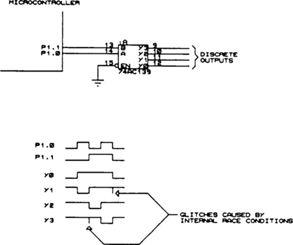
The timing diagram in the figure shows what happens as the microcontroller steps through the select lines. As each input line changes state, there is a momentary glitch at one or more outputs. The diagram shows glitches on the Y1 and Y3 outputs; this could vary from one manufacturer to another, based on the internal structure that each uses. Of course, if these outputs are driving registers or latches that are fast enough to respond to the glitches, the result could be invalid data in the registers. The solution to this particular problem is to use a third port pin, connected to the enable of the AC139, to gate the outputs off when the select inputs are being changed.
In Chapter 5, we’ll look at software debug.
*Note: This chapter refers to several test code fragments for the programmer. These are listed in Appendix 1, with selected portions of the programmer schematic.