
8.1 INTRODUCTION
Computer system performance depends on the memory system as well as the processor microarchitecture. Chapter 7 assumed an ideal memory system that could be accessed in a single clock cycle. However, this would be true only for a very small memory—or a very slow processor! Early processors were relatively slow, so memory was able to keep up. But processor speed has increased at a faster rate than memory speeds. DRAM memories are currently 10 to 100 times slower than processors. The increasing gap between processor and DRAM memory speeds demands increasingly ingenious memory systems to try to approximate a memory that is as fast as the processor. This chapter investigates practical memory systems and considers trade-offs of speed, capacity, and cost.
The processor communicates with the memory system over a memory interface. Figure 8.1 shows the simple memory interface used in our multicycle MIPS processor. The processor sends an address over the Address bus to the memory system. For a read, MemWrite is 0 and the memory returns the data on the ReadData bus. For a write, MemWrite is 1 and the processor sends data to memory on the WriteData bus.
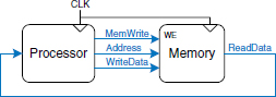
Figure 8.1 The memory interface
The major issues in memory system design can be broadly explained using a metaphor of books in a library. A library contains many books on the shelves. If you were writing a term paper on the meaning of dreams, you might go to the library1 and pull Freud’s The Interpretation of Dreams off the shelf and bring it to your cubicle. After skimming it, you might put it back and pull out Jung’s The Psychology of the Unconscious. You might then go back for another quote from Interpretation of Dreams, followed by yet another trip to the stacks for Freud’s The Ego and the Id. Pretty soon you would get tired of walking from your cubicle to the stacks. If you are clever, you would save time by keeping the books in your cubicle rather than schlepping them back and forth. Furthermore, when you pull a book by Freud, you could also pull several of his other books from the same shelf.
This metaphor emphasizes the principle, introduced in Section 6.2.1, of making the common case fast. By keeping books that you have recently used or might likely use in the future at your cubicle, you reduce the number of time-consuming trips to the stacks. In particular, you use the principles of temporal and spatial locality. Temporal locality means that if you have used a book recently, you are likely to use it again soon. Spatial locality means that when you use one particular book, you are likely to be interested in other books on the same shelf.
The library itself makes the common case fast by using these principles of locality. The library has neither the shelf space nor the budget to accommodate all of the books in the world. Instead, it keeps some of the lesser-used books in deep storage in the basement. Also, it may have an interlibrary loan agreement with nearby libraries so that it can offer more books than it physically carries.
In summary, you obtain the benefits of both a large collection and quick access to the most commonly used books through a hierarchy of storage. The most commonly used books are in your cubicle. A larger collection is on the shelves. And an even larger collection is available, with advanced notice, from the basement and other libraries. Similarly, memory systems use a hierarchy of storage to quickly access the most commonly used data while still having the capacity to store large amounts of data.
Memory subsystems used to build this hierarchy were introduced in Section 5.5. Computer memories are primarily built from dynamic RAM (DRAM) and static RAM (SRAM). Ideally, the computer memory system is fast, large, and cheap. In practice, a single memory only has two of these three attributes; it is either slow, small, or expensive. But computer systems can approximate the ideal by combining a fast small cheap memory and a slow large cheap memory. The fast memory stores the most commonly used data and instructions, so on average the memory system appears fast. The large memory stores the remainder of the data and instructions, so the overall capacity is large. The combination of two cheap memories is much less expensive than a single large fast memory. These principles extend to using an entire hierarchy of memories of increasing capacity and decreasing speed.
Computer memory is generally built from DRAM chips. In 2006, a typical PC had a main memory consisting of 256 MB to 1 GB of DRAM, and DRAM cost about $100 per gigabyte (GB). DRAM prices have declined at about 30% per year for the last three decades, and memory capacity has grown at the same rate, so the total cost of the memory in a PC has remained roughly constant. Unfortunately, DRAM speed has improved by only about 7% per year, whereas processor performance has improved at a rate of 30 to 50% per year, as shown in Figure 8.2. The plot shows memory and processor speeds with the 1980 speeds as a baseline. In about 1980, processor and memory speeds were the same. But performance has diverged since then, with memories badly lagging.
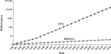
Figure 8.2 Diverging processor and memory performance Adapted with permission from Hennessy and Patterson, Computer Architecture: A Quantitative Approach, 3rd ed., Morgan Kaufmann, 2003.
DRAM could keep up with processors in the 1970s and early 1980’s, but it is now woefully too slow. The DRAM access time is one to two orders of magnitude longer than the processor cycle time (tens of nanoseconds, compared to less than one nanosecond).
To counteract this trend, computers store the most commonly used instructions and data in a faster but smaller memory, called a cache. The cache is usually built out of SRAM on the same chip as the processor. The cache speed is comparable to the processor speed, because SRAM is inherently faster than DRAM, and because the on-chip memory eliminates lengthy delays caused by traveling to and from a separate chip. In 2006, on-chip SRAM costs were on the order of $10,000/GB, but the cache is relatively small (kilobytes to a few megabytes), so the overall cost is low. Caches can store both instructions and data, but we will refer to their contents generically as “data.”
If the processor requests data that is available in the cache, it is returned quickly. This is called a cache hit. Otherwise, the processor retrieves the data from main memory (DRAM). This is called a cache miss. If the cache hits most of the time, then the processor seldom has to wait for the slow main memory, and the average access time is low.
The third level in the memory hierarchy is the hard disk, or hard drive. In the same way that a library uses the basement to store books that do not fit in the stacks, computer systems use the hard disk to store data that does not fit in main memory. In 2006, a hard disk cost less than $1/GB and had an access time of about 10 ms. Hard disk costs have decreased at 60%/year but access times scarcely improved. The hard disk provides an illusion of more capacity than actually exists in the main memory. It is thus called virtual memory. Like books in the basement, data in virtual memory takes a long time to access. Main memory, also called physical memory, holds a subset of the virtual memory. Hence, the main memory can be viewed as a cache for the most commonly used data from the hard disk.
Figure 8.3 summarizes the memory hierarchy of the computer system discussed in the rest of this chapter. The processor first seeks data in a small but fast cache that is usually located on the same chip. If the data is not available in the cache, the processor then looks in main memory. If the data is not there either, the processor fetches the data from virtual memory on the large but slow hard disk. Figure 8.4 illustrates this capacity and speed trade-off in the memory hierarchy and lists typical costs and access times in 2006 technology. As access time decreases, speed increases.
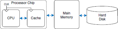
Figure 8.3 A typical memory hierarchy
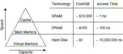
Figure 8.4 Memory hierarchy components, with typical characteristics in 2006
Section 8.2 introduces memory system performance analysis. Section 8.3 explores several cache organizations, and Section 8.4 delves into virtual memory systems. To conclude, this chapter explores how processors can access input and output devices, such as keyboards and monitors, in much the same way as they access memory. Section 8.5 investigates such memory-mapped I/O.
8.2 MEMORY SYSTEM PERFORMANCE ANALYSIS
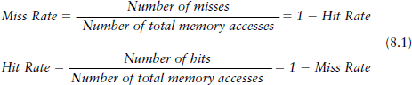
Designers (and computer buyers) need quantitative ways to measure the performance of memory systems to evaluate the cost-benefit trade-offs of various alternatives. Memory system performance metrics are miss rate or hit rate and average memory access time. Miss and hit rates are calculated as:
Example 8.1 CALCULATING CACHE PERFORMANCE
Suppose a program has 2000 data access instructions (loads or stores), and 1250 of these requested data values are found in the cache. The other 750 data values are supplied to the processor by main memory or disk memory. What are the miss and hit rates for the cache?
Solution: The miss rate is 750/2000 = 0.375 = 37.5%. The hit rate is 1250/2000 = 0.625 = 1 - 0.375 = 62.5%.
Average memory access time (AMAT) is the average time a processor must wait for memory per load or store instruction. In the typical computer system from Figure 8.3, the processor first looks for the data in the cache. If the cache misses, the processor then looks in main memory. If the main memory misses, the processor accesses virtual memory on the hard disk. Thus, AMAT is calculated as:
![]()
where tcache, tMM, and tVM are the access times of the cache, main memory, and virtual memory, and MRcache and MRMM are the cache and main memory miss rates, respectively.
Example 8.2 CALCULATING AVERAGE MEMORY ACCESS TIME
Suppose a computer system has a memory organization with only two levels of hierarchy, a cache and main memory. What is the average memory access time given the access times and miss rates given in Table 8.1?
Solution: The average memory access time is 1 + 0.1(100) = 11 cycles.
Table 8.1 Access times and miss rates
| Memory Level | Access Time (Cycles) | Miss Rate |
|---|---|---|
| Cache | 1 | 10% |
| Main Memory | 100 | 0% |
Gene Amdahl, 1922–. Most famous for Amdahl’s Law, an observation he made in 1965. While in graduate school, he began designing computers in his free time. This side work earned him his Ph.D. in theoretical physics in 1952. He joined IBM immediately after graduation, and later went on to found three companies, including one called Amdahl Corporation in 1970.
Example 8.3 IMPROVING ACCESS TIME
An 11-cycle average memory access time means that the processor spends ten cycles waiting for data for every one cycle actually using that data. What cache miss rate is needed to reduce the average memory access time to 1.5 cycles given the access times in Table 8.1?
Solution: If the miss rate is m, the average access time is 1 + 100m. Setting this time to 1.5 and solving for m requires a cache miss rate of 0.5%.
As a word of caution, performance improvements might not always be as good as they sound. For example, making the memory system ten times faster will not necessarily make a computer program run ten times as fast. If 50% of a program’s instructions are loads and stores, a tenfold memory system improvement only means a 1.82-fold improvement in program performance. This general principle is called Amdahl’s Law, which says that the effort spent on increasing the performance of a subsystem is worthwhile only if the subsystem affects a large percentage of the overall performance.
8.3 CACHES
A cache holds commonly used memory data. The number of data words that it can hold is called the capacity, C. Because the capacity of the cache is smaller than that of main memory, the computer system designer must choose what subset of the main memory is kept in the cache.
When the processor attempts to access data, it first checks the cache for the data. If the cache hits, the data is available immediately. If the cache misses, the processor fetches the data from main memory and places it in the cache for future use. To accommodate the new data, the cache must replace old data. This section investigates these issues in cache design by answering the following questions: (1) What data is held in the cache? (2) How is the data found? and (3) What data is replaced to make room for new data when the cache is full?
When reading the next sections, keep in mind that the driving force in answering these questions is the inherent spatial and temporal locality of data accesses in most applications. Caches use spatial and temporal locality to predict what data will be needed next. If a program accesses data in a random order, it would not benefit from a cache.
As we explain in the following sections, caches are specified by their capacity (C), number of sets (S), block size (b), number of blocks (B), and degree of associativity (N).
Although we focus on data cache loads, the same principles apply for fetches from an instruction cache. Data cache store operations are similar and are discussed further in Section 8.3.4.
Cache: a hiding place especially for concealing and preserving provisions or implements.
– Merriam Webster Online Dictionary. 2006. http://www.merriam-webster.com
8.3.1 What Data Is Held in the Cache?
An ideal cache would anticipate all of the data needed by the processor and fetch it from main memory ahead of time so that the cache has a zero miss rate. Because it is impossible to predict the future with perfect accuracy, the cache must guess what data will be needed based on the past pattern of memory accesses. In particular, the cache exploits temporal and spatial locality to achieve a low miss rate.
Recall that temporal locality means that the processor is likely to access a piece of data again soon if it has accessed that data recently. Therefore, when the processor loads or stores data that is not in the cache, the data is copied from main memory into the cache. Subsequent requests for that data hit in the cache.
Recall that spatial locality means that, when the processor accesses a piece of data, it is also likely to access data in nearby memory locations. Therefore, when the cache fetches one word from memory, it may also fetch several adjacent words. This group of words is called a cache block. The number of words in the cache block, b, is called the block size. A cache of capacity C contains B = C/b blocks.
The principles of temporal and spatial locality have been experimentally verified in real programs. If a variable is used in a program, the same variable is likely to be used again, creating temporal locality. If an element in an array is used, other elements in the same array are also likely to be used, creating spatial locality.
8.3.2 How Is the Data Found?
A cache is organized into S sets, each of which holds one or more blocks of data. The relationship between the address of data in main memory and the location of that data in the cache is called the mapping. Each memory address maps to exactly one set in the cache. Some of the address bits are used to determine which cache set contains the data. If the set contains more than one block, the data may be kept in any of the blocks in the set.
Caches are categorized based on the number of blocks in a set. In a direct mapped cache, each set contains exactly one block, so the cache has S = B sets. Thus, a particular main memory address maps to a unique block in the cache. In an N-way set associative cache, each set contains N blocks. The address still maps to a unique set, with S = B/N sets. But the data from that address can go in any of the N blocks in that set. A fully associative cache has only S = 1 set. Data can go in any of the B blocks in the set. Hence, a fully associative cache is another name for a B-way set associative cache.
To illustrate these cache organizations, we will consider a MIPS memory system with 32-bit addresses and 32-bit words. The memory is byte-addressable, and each word is four bytes, so the memory consists of 2 words aligned on word boundaries. We analyze caches with an eight-word capacity (C) for the sake of simplicity. We begin with a one-word block size (b), then generalize later to larger blocks.
Direct Mapped Cache
A direct mapped cache has one block in each set, so it is organized into S = B sets. To understand the mapping of memory addresses onto cache blocks, imagine main memory as being mapped into b-word blocks, just as the cache is. An address in block 0 of main memory maps to set 0 of the cache. An address in block 1 of main memory maps to set 1 of the cache, and so forth until an address in block B - 1 of main memory maps to block B - 1 of the cache. There are no more blocks of the cache, so the mapping wraps around, such that block B of main memory maps to block 0 of the cache.
This mapping is illustrated in Figure 8.5 for a direct mapped cache with a capacity of eight words and a block size of one word. The cache has eight sets, each of which contains a one-word block. The bottom two bits of the address are always 00, because they are word aligned. The next log28 = 3 bits indicate the set onto which the memory address maps. Thus, the data at addresses 0x00000004, 0x00000024,…, 0xFFFFFFE4 all map to set 1, as shown in blue. Likewise, data at addresses 0x00000010,…, 0xFFFFFFF0 all map to set 4, and so forth. Each main memory address maps to exactly one set in the cache.
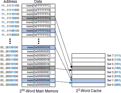
Figure 8.5 Mapping of main memory to a direct mapped cache
Example 8.4 CACHE FIELDS
To what cache set in Figure 8.5 does the word at address 0x00000014 map? Name another address that maps to the same set.
Solution: The two least significant bits of the address are 00, because the address is word aligned. The next three bits are 101, so the word maps to set 5. Words at addresses 0x34, 0x54, 0x74,…, 0xFFFFFFF4 all map to this same set.
Because many addresses map to a single set, the cache must also keep track of the address of the data actually contained in each set. The least significant bits of the address specify which set holds the data. The remaining most significant bits are called the tag and indicate which of the many possible addresses is held in that set.
In our previous example, the two least significant bits of the 32-bit address are called the byte offset, because they indicate the byte within the word. The next three bits are called the set bits, because they indicate the set to which the address maps. (In general, the number of set bits is log2S.) The remaining 27 tag bits indicate the memory address of the data stored in a given cache set. Figure 8.6 shows the cache fields for address 0xFFFFFFE4. It maps to set 1 and its tag is all 1’s.
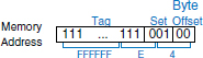
Figure 8.6 Cache fields for address 0xFFFFFFE4 when mapping to the cache in Figure 8.5
Find the number of set and tag bits for a direct mapped cache with 1024 (210) sets and a one-word block size. The address size is 32 bits.
Solution: A cache with 210 sets requires log2(210) = 10 set bits. The two least significant bits of the address are the byte offset, and the remaining 32 - 10 - 2 = 20 bits form the tag.
Sometimes, such as when the computer first starts up, the cache sets contain no data at all. The cache uses a valid bit for each set to indicate whether the set holds meaningful data. If the valid bit is 0, the contents are meaningless.
Figure 8.7 shows the hardware for the direct mapped cache of Figure 8.5. The cache is constructed as an eight-entry SRAM. Each entry, or set, contains one line consisting of 32 bits of data, 27 bits of tag, and 1 valid bit. The cache is accessed using the 32-bit address. The two least significant bits, the byte offset bits, are ignored for word accesses. The next three bits, the set bits, specify the entry or set in the cache. A load instruction reads the specified entry from the cache and checks the tag and valid bits. If the tag matches the most significant 27 bits of the address and the valid bit is 1, the cache hits and the data is returned to the processor. Otherwise, the cache misses and the memory system must fetch the data from main memory.
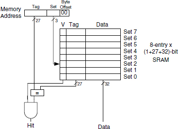
Figure 8.7 Direct mapped cache with 8 sets
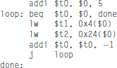
Example 8.6 TEMPORAL LOCALITY WITH A DIRECT MAPPED CACHE
Loops are a common source of temporal and spatial locality in applications. Using the eight-entry cache of Figure 8.7, show the contents of the cache after executing the following silly loop in MIPS assembly code. Assume that the cache is initially empty. What is the miss rate?
Solution: The program contains a loop that repeats for five iterations. Each iteration involves three memory accesses (loads), resulting in 15 total memory accesses. The first time the loop executes, the cache is empty and the data must be fetched from main memory locations 0x4, 0xC, and 0x8 into cache sets 1, 3, and 2, respectively. However, the next four times the loop executes, the data is found in the cache. Figure 8.8 shows the contents of the cache during the last request to memory address 0x4. The tags are all 0 because the upper 27 bits of the addresses are 0. The miss rate is 3/15 = 20%.
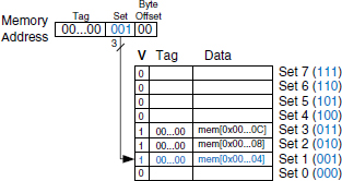
Figure 8.8 Direct mapped cache contents
When two recently accessed addresses map to the same cache block, a conflict occurs, and the most recently accessed address evicts the previous one from the block. Direct mapped caches have only one block in each set, so two addresses that map to the same set always cause a conflict. The example on the next page illustrates conflicts.
Example 8.7 CACHE BLOCK CONFLICT
What is the miss rate when the following loop is executed on the eight-word direct mapped cache from Figure 8.7? Assume that the cache is initially empty.
Solution: Memory addresses 0x4 and 0x24 both map to set 1. During the initial execution of the loop, data at address 0x4 is loaded into set 1 of the cache. Then data at address 0x24 is loaded into set 1, evicting the data from address 0x4. Upon the second execution of the loop, the pattern repeats and the cache must refetch data at address 0x4, evicting data from address 0x24. The two addresses conflict, and the miss rate is 100%.
Multi-way Set Associative Cache
An N-way set associative cache reduces conflicts by providing N blocks in each set where data mapping to that set might be found. Each memory address still maps to a specific set, but it can map to any one of the N blocks in the set. Hence, a direct mapped cache is another name for a one-way set associative cache. N is also called the degree of associativity of the cache.
Figure 8.9 shows the hardware for a C = 8-word, N = 2-way set associative cache. The cache now has only S = 4 sets rather than 8.
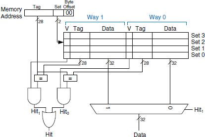
Figure 8.9 Two-way set associative cache
Thus, only log24 = 2 set bits rather than 3 are used to select the set. The tag increases from 27 to 28 bits. Each set contains two ways or degrees of associativity. Each way consists of a data block and the valid and tag bits. The cache reads blocks from both ways in the selected set and checks the tags and valid bits for a hit. If a hit occurs in one of the ways, a multiplexer selects data from that way.
Set associative caches generally have lower miss rates than direct mapped caches of the same capacity, because they have fewer conflicts. However, set associative caches are usually slower and somewhat more expensive to build because of the output multiplexer and additional comparators. They also raise the question of which way to replace when both ways are full; this is addressed further in Section 8.3.3. Most commercial systems use set associative caches.
Example 8.8 SET ASSOCIATIVE CACHE MISS RATE
Repeat Example 8.7 using the eight-word two-way set associative cache from Figure 8.9.
Solution: Both memory accesses, to addresses 0x4 and 0x24, map to set 1. However, the cache has two ways, so it can accommodate data from both addresses. During the first loop iteration, the empty cache misses both addresses and loads both words of data into the two ways of set 1, as shown in Figure 8.10. On the next four iterations, the cache hits. Hence, the miss rate is 2/10 = 20%. Recall that the direct mapped cache of the same size from Example 8.7 had a miss rate of 100%.
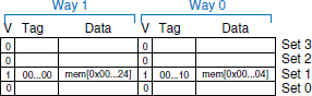
Figure 8.10 Two-way set associative cache contents
Fully Associative Cache
A fully associative cache contains a single set with B ways, where B is the number of blocks. A memory address can map to a block in any of these ways. A fully associative cache is another name for a B-way set associative cache with one set.
Figure 8.11 shows the SRAM array of a fully associative cache with eight blocks. Upon a data request, eight tag comparisons (not shown) must be made, because the data could be in any block. Similarly, an 8:1 multiplexer chooses the proper data if a hit occurs. Fully associative caches tend to have the fewest conflict misses for a given cache capacity, but they require more hardware for additional tag comparisons. They are best suited to relatively small caches because of the large number of comparators.
Figure 8.11 Eight-block fully associative cache
Block Size
The previous examples were able to take advantage only of temporal locality, because the block size was one word. To exploit spatial locality, a cache uses larger blocks to hold several consecutive words.
The advantage of a block size greater than one is that when a miss occurs and the word is fetched into the cache, the adjacent words in the block are also fetched. Therefore, subsequent accesses are more likely to hit because of spatial locality. However, a large block size means that a fixed-size cache will have fewer blocks. This may lead to more conflicts, increasing the miss rate. Moreover, it takes more time to fetch the missing cache block after a miss, because more than one data word is fetched from main memory. The time required to load the missing block into the cache is called the miss penalty. If the adjacent words in the block are not accessed later, the effort of fetching them is wasted. Nevertheless, most real programs benefit from larger block sizes.
Figure 8.12 shows the hardware for a C = 8-word direct mapped cache with a b = 4-word block size. The cache now has only B = C/b = 2 blocks. A direct mapped cache has one block in each set, so this cache is organized as two sets. Thus, only log22 = 1 bit is used to select the set. A multiplexer is now needed to select the word within the block. The multiplexer is controlled by the log24 = 2 block offset bits of the address. The most significant 27 address bits form the tag. Only one tag is needed for the entire block, because the words in the block are at consecutive addresses.
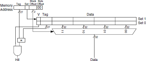
Figure 8.12 Direct mapped cache with two sets and a four-word block size
Figure 8.13 shows the cache fields for address 0x8000009C when it maps to the direct mapped cache of Figure 8.12. The byte offset bits are always 0 for word accesses. The next log2b = 2 block offset bits indicate the word within the block. And the next bit indicates the set. The remaining 27 bits are the tag. Therefore, word 0x8000009C maps to set 1, word 3 in the cache. The principle of using larger block sizes to exploit spatial locality also applies to associative caches.
Figure 8.13 Cache fields for address 0x8000009C when mapping to the cache of Figure 8.12
Example 8.9 SPATIAL LOCALITY WITH A DIRECT MAPPED CACHE
Repeat Example 8.6 for the eight-word direct mapped cache with a four-word block size.
Solution: Figure 8.14 shows the contents of the cache after the first memory access. On the first loop iteration, the cache misses on the access to memory address 0x4. This access loads data at addresses 0x0 through 0xC into the cache block. All subsequent accesses (as shown for address 0xC) hit in the cache. Hence, the miss rate is 1/15 = 6.67%.
Figure 8.14 Cache contents with a block size (b) of four words
Putting It All Together
Caches are organized as two-dimensional arrays. The rows are called sets, and the columns are called ways. Each entry in the array consists of a data block and its associated valid and tag bits. Caches are characterized by
Table 8.2 Cache organizations
| Organization | Number of Ways (N) | Number of Sets (S) |
|---|---|---|
| direct mapped | 1 | B |
| set associative | 1 < N < B | B/N |
| fully associative | B | 1 |
Table 8.2 summarizes the various cache organizations. Each address in memory maps to only one set but can be stored in any of the ways.
Cache capacity, associativity, set size, and block size are typically powers of 2. This makes the cache fields (tag, set, and block offset bits) subsets of the address bits.
Increasing the associativity, N, usually reduces the miss rate caused by conflicts. But higher associativity requires more tag comparators. Increasing the block size, b, takes advantage of spatial locality to reduce the miss rate. However, it decreases the number of sets in a fixed sized cache and therefore could lead to more conflicts. It also increases the miss penalty.
8.3.3 What Data Is Replaced?
In a direct mapped cache, each address maps to a unique block and set. If a set is full when new data must be loaded, the block in that set is replaced with the new data. In set associative and fully associative caches, the cache must choose which block to evict when a cache set is full. The principle of temporal locality suggests that the best choice is to evict the least recently used block, because it is least likely to be used again soon. Hence, most associative caches have a least recently used (LRU) replacement policy.
In a two-way set associative cache, a use bit, U, indicates which way within a set was least recently used. Each time one of the ways is used, U is adjusted to indicate the other way. For set associative caches with more than two ways, tracking the least recently used way becomes complicated. To simplify the problem, the ways are often divided into two groups and U indicates which group of ways was least recently used. Upon replacement, the new block replaces a random block within the least recently used group. Such a policy is called pseudo-LRU and is good enough in practice.
Example 8.10 LRU REPLACEMENT
Show the contents of an eight-word two-way set associative cache after executing the following code. Assume LRU replacement, a block size of one word, and an initially empty cache.
Solution: The first two instructions load data from memory addresses 0x4 and 0x24 into set 1 of the cache, shown in Figure 8.15(a). U = 0 indicates that data in way 0 was the least recently used. The next memory access, to address 0x54, also maps to set 1 and replaces the least recently used data in way 0, as shown in Figure 8.15(b), The use bit, U, is set to 1 to indicate that data in way 1 was the least recently used.
Figure 8.15 Two-way associative cache with LRU replacement
8.3.4 Advanced Cache Design*
Modern systems use multiple levels of caches to decrease memory access time. This section explores the performance of a two-level caching system and examines how block size, associativity, and cache capacity affect miss rate. The section also describes how caches handle stores, or writes, by using a write-through or write-back policy.
Multiple-Level Caches
Large caches are beneficial because they are more likely to hold data of interest and therefore have lower miss rates. However, large caches tend to be slower than small ones. Modern systems often use two levels of caches, as shown in Figure 8.16. The first-level (L1) cache is small enough to provide a one- or two-cycle access time. The second-level (L2) cache is also built from SRAM but is larger, and therefore slower, than the L1 cache. The processor first looks for the data in the L1 cache. If the L1 cache misses, the processor looks in the L2 cache. If the L2 cache misses, the processor fetches the data from main memory. Some modern systems add even more levels of cache to the memory hierarchy, because accessing main memory is so slow.
Figure 8.16 Memory hierarchy with two levels of cache
Example 8.11 SYSTEM WITH AN L2 CACHE
Use the system of Figure 8.16 with access times of 1, 10, and 100 cycles for the L1 cache, L2 cache, and main memory, respectively. Assume that the L1 and L2 caches have miss rates of 5% and 20%, respectively. Specifically, of the 5% of accesses that miss the L1 cache, 20% of those also miss the L2 cache. What is the average memory access time (AMAT)?
Solution: Each memory access checks the L1 cache. When the L1 cache misses (5% of the time), the processor checks the L2 cache. When the L2 cache misses (20% of the time), the processor fetches the data from main memory. Using Equation 8.2, we calculate the average memory access time as follows: 1 cycle + 0.05[10 cycles + 0.2(100 cycles)] = 2.5 cycles
The L2 miss rate is high because it receives only the “hard” memory accesses, those that miss in the L1 cache. If all accesses went directly to the L2 cache, the L2 miss rate would be about 1%.
Reducing Miss Rate
Cache misses can be reduced by changing capacity, block size, and/or associativity. The first step to reducing the miss rate is to understand the causes of the misses. The misses can be classified as compulsory, capacity, and conflict. The first request to a cache block is called a compulsory miss, because the block must be read from memory regardless of the cache design. Capacity misses occur when the cache is too small to hold all concurrently used data. Conflict misses are caused when several addresses map to the same set and evict blocks that are still needed.
Changing cache parameters can affect one or more type of cache miss. For example, increasing cache capacity can reduce conflict and capacity misses, but it does not affect compulsory misses. On the other hand, increasing block size could reduce compulsory misses (due to spatial locality) but might actually increase conflict misses (because more addresses would map to the same set and could conflict).
Memory systems are complicated enough that the best way to evaluate their performance is by running benchmarks while varying cache parameters. Figure 8.17 plots miss rate versus cache size and degree of associativity for the SPEC2000 benchmark. This benchmark has a small number of compulsory misses, shown by the dark region near the x-axis. As expected, when cache size increases, capacity misses decrease. Increased associativity, especially for small caches, decreases the number of conflict misses shown along the top of the curve. Increasing associativity beyond four or eight ways provides only small decreases in miss rate.
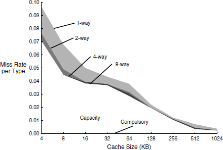
Figure 8.17 Miss rate versus cache size and associativity on SPEC2000 benchmark Adapted with permission from Hennessy and Patterson, Computer Architecture: A Quantitative Approach, 3rd ed., Morgan Kaufmann, 2003.
As mentioned, miss rate can also be decreased by using larger block sizes that take advantage of spatial locality. But as block size increases, the number of sets in a fixed size cache decreases, increasing the probability of conflicts. Figure 8.18 plots miss rate versus block size (in number of bytes) for caches of varying capacity. For small caches, such as the 4-KB cache, increasing the block size beyond 64 bytes increases the miss rate because of conflicts. For larger caches, increasing the block size does not change the miss rate. However, large block sizes might still increase execution time because of the larger miss penalty, the time required to fetch the missing cache block from main memory on a miss.
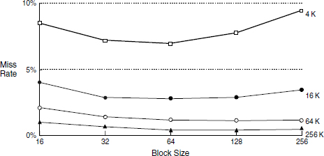
Figure 8.18 Miss rate versus block size and cache size on SPEC92 benchmark Adapted with permission from Hennessy and Patterson, Computer Architecture: A Quantitative Approach, 3rd ed., Morgan Kaufmann, 2003.
Write Policy
The previous sections focused on memory loads. Memory stores, or writes, follow a similar procedure as loads. Upon a memory store, the processor checks the cache. If the cache misses, the cache block is fetched from main memory into the cache, and then the appropriate word in the cache block is written. If the cache hits, the word is simply written to the cache block.
Caches are classified as either write-through or write-back. In a write-through cache, the data written to a cache block is simultaneously written to main memory. In a write-back cache, a dirty bit (D) is associated with each cache block. D is 1 when the cache block has been written and 0 otherwise. Dirty cache blocks are written back to main memory only when they are evicted from the cache. A write-through cache requires no dirty bit but usually requires more main memory writes than a write-back cache. Modern caches are usually write-back, because main memory access time is so large.
Example 8.12 WRITE-THROUGH VERSUS WRITE-BACK
Suppose a cache has a block size of four words. How many main memory accesses are required by the following code when using each write policy: write-through or write-back?
Solution: All four store instructions write to the same cache block. With a write-through cache, each store instruction writes a word to main memory, requiring four main memory writes. A write-back policy requires only one main memory access, when the dirty cache block is evicted.
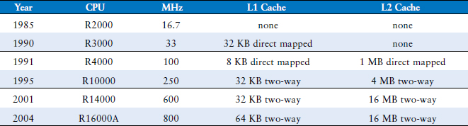
8.3.5 The Evolution of MIPS Caches*
Table 8.3 traces the evolution of cache organizations used by the MIPS processor from 1985 to 2004. The major trends are the introduction of multiple levels of cache, larger cache capacity, and increased associativity. These trends are driven by the growing disparity between CPU frequency and main memory speed and the decreasing cost of transistors. The growing difference between CPU and memory speeds necessitates a lower miss rate to avoid the main memory bottleneck, and the decreasing cost of transistors allows larger cache sizes.
Table 8.3 MIPS cache evolution*
* Adapted from D. Sweetman, See MIPS Run, Morgan Kaufmann, 1999.
8.4 VIRTUAL MEMORY
Most modern computer systems use a hard disk (also called a hard drive) as the lowest level in the memory hierarchy (see Figure 8.4). Compared with the ideal large, fast, cheap memory, a hard disk is large and cheap but terribly slow. The disk provides a much larger capacity than is possible with a cost-effective main memory (DRAM). However, if a significant fraction of memory accesses involve the disk, performance is dismal. You may have encountered this on a PC when running too many programs at once.
Figure 8.19 shows a hard disk with the lid of its case removed. As the name implies, the hard disk contains one or more rigid disks or platters, each of which has a read/write head on the end of a long triangular arm. The head moves to the correct location on the disk and reads or writes data magnetically as the disk rotates beneath it. The head takes several milliseconds to seek the correct location on the disk, which is fast from a human perspective but millions of times slower than the processor.
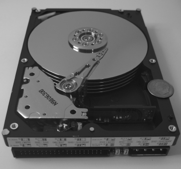
Figure 8.19 Hard disk
The objective of adding a hard disk to the memory hierarchy is to inexpensively give the illusion of a very large memory while still providing the speed of faster memory for most accesses. A computer with only 128 MB of DRAM, for example, could effectively provide 2 GB of memory using the hard disk. This larger 2-GB memory is called virtual memory, and the smaller 128-MB main memory is called physical memory. We will use the term physical memory to refer to main memory throughout this section.
A computer with 32-bit addresses can access a maximum of 232 bytes = 4 GB of memory. This is one of the motivations for moving to 64-bit computers, which can access far more memory.
Programs can access data anywhere in virtual memory, so they must use virtual addresses that specify the location in virtual memory. The physical memory holds a subset of most recently accessed virtual memory. In this way, physical memory acts as a cache for virtual memory. Thus, most accesses hit in physical memory at the speed of DRAM, yet the program enjoys the capacity of the larger virtual memory.
Virtual memory systems use different terminologies for the same caching principles discussed in Section 8.3. Table 8.4 summarizes the analogous terms. Virtual memory is divided into virtual pages, typically 4 KB in size. Physical memory is likewise divided into physical pages of the same size. A virtual page may be located in physical memory (DRAM) or on the disk. For example, Figure 8.20 shows a virtual memory that is larger than physical memory. The rectangles indicate pages. Some virtual pages are present in physical memory, and some are located on the disk. The process of determining the physical address from the virtual address is called address translation. If the processor attempts to access a virtual address that is not in physical memory, a page fault occurs, and the operating system loads the page from the hard disk into physical memory.
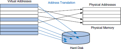
Figure 8.20 Virtual and physical pages
To avoid page faults caused by conflicts, any virtual page can map to any physical page. In other words, physical memory behaves as a fully associative cache for virtual memory. In a conventional fully associative cache, every cache block has a comparator that checks the most significant address bits against a tag to determine whether the request hits in the block. In an analogous virtual memory system, each physical page would need a comparator to check the most significant virtual address bits against a tag to determine whether the virtual page maps to that physical page.
Table 8.4 Analogous cache and virtual memory terms
| Cache | Virtual Memory |
|---|---|
| Block | Page |
| Block size | Page size |
| Block offset | Page offset |
| Miss | Page fault |
| Tag | Virtual page number |
A realistic virtual memory system has so many physical pages that providing a comparator for each page would be excessively expensive. Instead, the virtual memory system uses a page table to perform address translation. A page table contains an entry for each virtual page, indicating its location in physical memory or that it is on the disk. Each load or store instruction requires a page table access followed by a physical memory access. The page table access translates the virtual address used by the program to a physical address. The physical address is then used to actually read or write the data.
The page table is usually so large that it is located in physical memory. Hence, each load or store involves two physical memory accesses: a page table access, and a data access. To speed up address translation, a translation lookaside buffer (TLB) caches the most commonly used page table entries.
The remainder of this section elaborates on address translation, page tables, and TLBs.
8.4.1 Address Translation
In a system with virtual memory, programs use virtual addresses so that they can access a large memory. The computer must translate these virtual addresses to either find the address in physical memory or take a page fault and fetch the data from the hard disk.
Recall that virtual memory and physical memory are divided into pages. The most significant bits of the virtual or physical address specify the virtual or physical page number. The least significant bits specify the word within the page and are called the page offset.
Figure 8.21 illustrates the page organization of a virtual memory system with 2 GB of virtual memory and 128 MB of physical memory divided into 4-KB pages. MIPS accommodates 32-bit addresses. With a 2-GB = 231-byte virtual memory, only the least significant 31 virtual address bits are used; the 32nd bit is always 0. Similarly, with a 128-MB = 227-byte physical memory, only the least significant 27 physical address bits are used; the upper 5 bits are always 0.
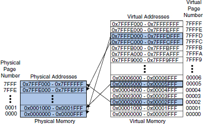
Figure 8.21 Physical and virtual pages
Because the page size is 4 KB = 212 bytes, there are 231/212 = 219 virtual pages and 227/212 = 215 physical pages. Thus, the virtual and physical page numbers are 19 and 15 bits, respectively. Physical memory can only hold up to 1/16th of the virtual pages at any given time. The rest of the virtual pages are kept on disk.
Figure 8.21 shows virtual page 5 mapping to physical page 1, virtual page 0x7FFFC mapping to physical page 0x7FFE, and so forth. For example, virtual address 0x53F8 (an offset of 0x3F8 within virtual page 5) maps to physical address 0x13F8 (an offset of 0x3F8 within physical page 1). The least significant 12 bits of the virtual and physical addresses are the same (0x3F8) and specify the page offset within the virtual and physical pages. Only the page number needs to be translated to obtain the physical address from the virtual address.
Figure 8.22 illustrates the translation of a virtual address to a physical address. The least significant 12 bits indicate the page offset and require no translation. The upper 19 bits of the virtual address specify the virtual page number (VPN) and are translated to a 15-bit physical page number (PPN). The next two sections describe how page tables and TLBs are used to perform this address translation.
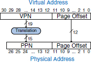
Figure 8.22 Translation from virtual address to physical address
Example 8.13 VIRTUAL ADDRESS TO PHYSICAL ADDRESS TRANSLATION
Find the physical address of virtual address 0x247C using the virtual memory system shown in Figure 8.21.
Solution: The 12-bit page offset (0x47C) requires no translation. The remaining 19 bits of the virtual address give the virtual page number, so virtual address 0x247C is found in virtual page 0x2. In Figure 8.21, virtual page 0x2 maps to physical page 0x7FFF. Thus, virtual address 0x247C maps to physical address 0x7FFF47C.
8.4.2 The Page Table
The processor uses a page table to translate virtual addresses to physical addresses. Recall that the page table contains an entry for each virtual page. This entry contains a physical page number and a valid bit. If the valid bit is 1, the virtual page maps to the physical page specified in the entry. Otherwise, the virtual page is found on disk.
Because the page table is so large, it is stored in physical memory. Let us assume for now that it is stored as a contiguous array, as shown in Figure 8.23. This page table contains the mapping of the memory system of Figure 8.21. The page table is indexed with the virtual page number (VPN). For example, entry 5 specifies that virtual page 5 maps to physical page 1. Entry 6 is invalid (V = 0), so virtual page 6 is located on disk.
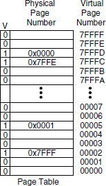
Figure 8.23 The page table for Figure 8.21
Example 8.14 USING THE PAGE TABLE TO PERFORM ADDRESS TRANSLATION
Find the physical address of virtual address 0x247C using the page table shown in Figure 8.23.
Solution: Figure 8.24 shows the virtual address to physical address translation for virtual address 0x247C. The 12-bit page offset requires no translation. The remaining 19 bits of the virtual address are the virtual page number, 0x2, and give the index into the page table. The page table maps virtual page 0x2 to physical page 0x7FFF. So, virtual address 0x247C maps to physical address 0x7FFF47C. The least significant 12 bits are the same in both the physical and the virtual address.
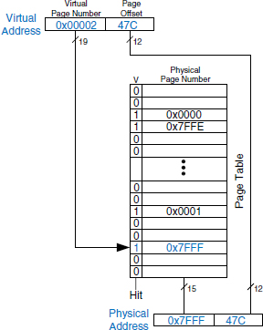
Figure 8.24 Address translation using the page table
The page table can be stored anywhere in physical memory, at the discretion of the OS. The processor typically uses a dedicated register, called the page table register, to store the base address of the page table in physical memory.
To perform a load or store, the processor must first translate the virtual address to a physical address and then access the data at that physical address. The processor extracts the virtual page number from the virtual address and adds it to the page table register to find the physical address of the page table entry. The processor then reads this page table entry from physical memory to obtain the physical page number. If the entry is valid, it merges this physical page number with the page offset to create the physical address. Finally, it reads or writes data at this physical address. Because the page table is stored in physical memory, each load or store involves two physical memory accesses.
8.4.3 The Translation Lookaside Buffer
Virtual memory would have a severe performance impact if it required a page table read on every load or store, doubling the delay of loads and stores. Fortunately, page table accesses have great temporal locality. The temporal and spatial locality of data accesses and the large page size mean that many consecutive loads or stores are likely to reference the same page. Therefore, if the processor remembers the last page table entry that it read, it can probably reuse this translation without rereading the page table. In general, the processor can keep the last several page table entries in a small cache called a translation lookaside buffer (TLB). The processor “looks aside” to find the translation in the TLB before having to access the page table in physical memory. In real programs, the vast majority of accesses hit in the TLB, avoiding the time-consuming page table reads from physical memory.
A TLB is organized as a fully associative cache and typically holds 16 to 512 entries. Each TLB entry holds a virtual page number and its corresponding physical page number. The TLB is accessed using the virtual page number. If the TLB hits, it returns the corresponding physical page number. Otherwise, the processor must read the page table in physical memory. The TLB is designed to be small enough that it can be accessed in less than one cycle. Even so, TLBs typically have a hit rate of greater than 99%. The TLB decreases the number of memory accesses required for most load or store instructions from two to one.
Example 8.15 USING THE TLB TO PERFORM ADDRESS TRANSLATION
Consider the virtual memory system of Figure 8.21. Use a two-entry TLB or explain why a page table access is necessary to translate virtual addresses 0x247C and 0x5FB0 to physical addresses. Suppose the TLB currently holds valid translations of virtual pages 0x2 and 0x7FFFD.
Solution: Figure 8.25 shows the two-entry TLB with the request for virtual address 0x247C. The TLB receives the virtual page number of the incoming address, 0x2, and compares it to the virtual page number of each entry. Entry 0 matches and is valid, so the request hits. The translated physical address is the physical page number of the matching entry, 0x7FFF, concatenated with the page offset of the virtual address. As always, the page offset requires no translation.
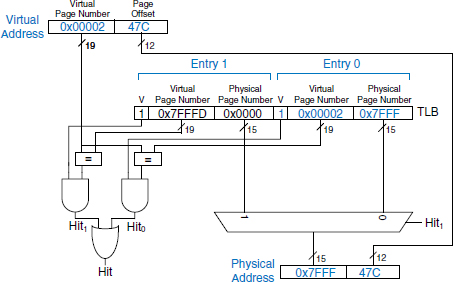
Figure 8.25 Address translation using a two-entry TLB
The request for virtual address 0x5FB0 misses in the TLB. So, the request is forwarded to the page table for translation.
8.4.4 Memory Protection
So far this section has focused on using virtual memory to provide a fast, inexpensive, large memory. An equally important reason to use virtual memory is to provide protection between concurrently running programs.
As you probably know, modern computers typically run several programs or processes at the same time. All of the programs are simultaneously present in physical memory. In a well-designed computer system, the programs should be protected from each other so that no program can crash or hijack another program. Specifically, no program should be able to access another program’s memory without permission. This is called memory protection.
Virtual memory systems provide memory protection by giving each program its own virtual address space. Each program can use as much memory as it wants in that virtual address space, but only a portion of the virtual address space is in physical memory at any given time. Each program can use its entire virtual address space without having to worry about where other programs are physically located. However, a program can access only those physical pages that are mapped in its page table. In this way, a program cannot accidentally or maliciously access another program’s physical pages, because they are not mapped in its page table. In some cases, multiple programs access common instructions or data. The operating system adds control bits to each page table entry to determine which programs, if any, can write to the shared physical pages.
8.4.5 Replacement Policies*
Virtual memory systems use write-back and an approximate least recently used (LRU) replacement policy. A write-through policy, where each write to physical memory initiates a write to disk, would be impractical. Store instructions would operate at the speed of the disk instead of the speed of the processor (milliseconds instead of nanoseconds). Under the writeback policy, the physical page is written back to disk only when it is evicted from physical memory. Writing the physical page back to disk and reloading it with a different virtual page is called swapping, so the disk in a virtual memory system is sometimes called swap space. The processor swaps out one of the least recently used physical pages when a page fault occurs, then replaces that page with the missing virtual page. To support these replacement policies, each page table entry contains two additional status bits: a dirty bit, D, and a use bit, U.
The dirty bit is 1 if any store instructions have changed the physical page since it was read from disk. When a physical page is swapped out, it needs to be written back to disk only if its dirty bit is 1; otherwise, the disk already holds an exact copy of the page.
The use bit is 1 if the physical page has been accessed recently. As in a cache system, exact LRU replacement would be impractically complicated. Instead, the OS approximates LRU replacement by periodically resetting all the use bits in the page table. When a page is accessed, its use bit is set to 1. Upon a page fault, the OS finds a page with U = 0 to swap out of physical memory. Thus, it does not necessarily replace the least recently used page, just one of the least recently used pages.
8.4.6 Multilevel Page Tables*
Page tables can occupy a large amount of physical memory. For example, the page table from the previous sections for a 2 GB virtual memory with 4 KB pages would need 219 entries. If each entry is 4 bytes, the page table is 219 X 22 bytes = 221 bytes = 2 MB.
To conserve physical memory, page tables can be broken up into multiple (usually two) levels. The first-level page table is always kept in physical memory. It indicates where small second-level page tables are stored in virtual memory. The second-level page tables each contain the actual translations for a range of virtual pages. If a particular range of translations is not actively used, the corresponding second-level page table can be swapped out to the hard disk so it does not waste physical memory.
In a two-level page table, the virtual page number is split into two parts: the page table number and the page table offset, as shown in Figure 8.26. The page table number indexes the first-level page table, which must reside in physical memory. The first-level page table entry gives the base address of the second-level page table or indicates that it must be fetched from disk when V is 0. The page table offset indexes the second-level page table. The remaining 12 bits of the virtual address are the page offset, as before, for a page size of 212 = 4 KB.
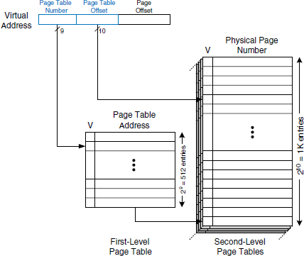
Figure 8.26 Hierarchical page tables
In Figure 8.26 the 19-bit virtual page number is broken into 9 and 10 bits, to indicate the page table number and the page table offset, respectively. Thus, the first-level page table has 29 = 512 entries. Each of these 512 second-level page tables has 210 = 1 K entries. If each of the first- and second-level page table entries is 32 bits (4 bytes) and only two second-level page tables are present in physical memory at once, the hierarchical page table uses only (512 X 4 bytes) + 2 X (1 K X 4 bytes) = 10 KB of physical memory. The two-level page table requires a fraction of the physical memory needed to store the entire page table (2 MB). The drawback of a two-level page table is that it adds yet another memory access for translation when the TLB misses.
Example 8.16 USING A MULTILEVEL PAGE TABLE FOR ADDRESS TRANSLATION
Figure 8.27 shows the possible contents of the two-level page table from Figure 8.26. The contents of only one second-level page table are shown. Using this two-level page table, describe what happens on an access to virtual address 0x003FEFB0.
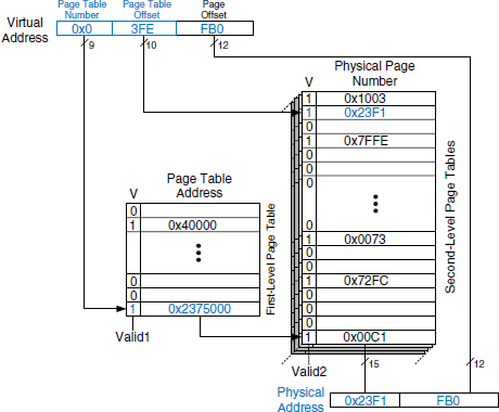
Figure 8.27 Address translation using a two-level page table
Solution: As always, only the virtual page number requires translation. The most significant nine bits of the virtual address, 0x0, give the page table number, the index into the first-level page table. The first-level page table at entry 0x0 indicates that the second-level page table is resident in memory (V = 1) and its physical address is 0x2375000.
The next ten bits of the virtual address, 0x3FE, are the page table offset, which gives the index into the second-level page table. Entry 0 is at the bottom of the second-level page table, and entry 0x3FF is at the top. Entry 0x3FE in the second-level page table indicates that the virtual page is resident in physical memory (V = 1) and that the physical page number is 0x23F1. The physical page number is concatenated with the page offset to form the physical address, 0x23F1FB0.
8.5 MEMORY-MAPPED I/O*
Processors also use the memory interface to communicate with input/output (I/O) devices such as keyboards, monitors, and printers. A processor accesses an I/O device using the address and data busses in the same way that it accesses memory.
A portion of the address space is dedicated to I/O devices rather than memory. For example, suppose that addresses in the range 0xFFFF0000 to 0xFFFFFFFF are used for I/O. Recall from Section 6.6.1 that these addresses are in a reserved portion of the memory map. Each I/O device is assigned one or more memory addresses in this range. A store to the specified address sends data to the device. A load receives data from the device. This method of communicating with I/O devices is called memory-mapped I/O.
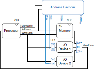
Figure 8.28 Support hardware for memory-mapped I/O
In a system with memory-mapped I/O, a load or store may access either memory or an I/O device. Figure 8.28 shows the hardware needed to support two memory-mapped I/O devices. An address decoder determines which device communicates with the processor. It uses the Address and MemWrite signals to generate control signals for the rest of the hardware. The ReadData multiplexer selects between memory and the various I/O devices. Write-enabled registers hold the values written to the I/O devices.
Some architectures, notably IA-32, use specialized instructions instead of memory-mapped I/O to communicate with I/O devices. These instructions are of the following form, where device1 and device2 are the unique ID of the peripheral device:
lwio $t0, device1
swio $t0, device2
This type of communication with I/O devices is called programmed I/O.
Example 8.17 COMMUNICATING WITH I/O DEVICES
Suppose I/O Device 1 in Figure 8.28 is assigned the memory address 0xFFFFFFF4. Show the MIPS assembly code for writing the value 7 to I/O Device 1 and for reading the output value from I/O Device 1.
Solution: The following MIPS assembly code writes the value 7 to I/O Device 1.2
addi $t0, $0, 7
sw $t0, 0xFFF4($0)
The address decoder asserts WE1 because the address is 0xFFFFFFF4 and MemWrite is TRUE. The value on the WriteData bus, 7, is written into the register connected to the input pins of I/O Device 1.
To read from I/O Device 1, the processor performs the following MIPS assembly code.
lw $t1, 0xFFF4($0)
The address decoder sets RDsel1:0 to 01, because it detects the address 0xFFFFFFF4 and MemWrite is FALSE. The output of I/O Device 1 passes through the multiplexer onto the ReadData bus and is loaded into $t1 in the processor.
Software that communicates with an I/O device is called a device driver. You have probably downloaded or installed device drivers for your printer or other I/O device. Writing a device driver requires detailed knowledge about the I/O device hardware. Other programs call functions in the device driver to access the device without having to understand the low-level device hardware.
To illustrate memory-mapped I/O hardware and software, the rest of this section describes interfacing a commercial speech synthesizer chip to a MIPS processor.
See www.speechchips.com for more information about the SP0256 and the allophone encodings.
Speech Synthesizer Hardware
The Radio Shack SP0256 speech synthesizer chip generates robot-like speech. Words are composed of one or more allophones, the fundamental units of sound. For example, the word “hello” uses five allophones represented by the following symbols in the SP0256 speech chip: HH1 EH LL AX OW The speech synthesizer uses 6-bit codes to represent 64 different allophones that appear in the English language. For example, the five allophones for the word “hello” correspond to the hexadecimal values 0x1B, 0x07, 0x2D, 0x0F, 0x20, respectively. The processor sends a series of allophones to the speech synthesizer, which drives a speaker to blabber the sounds.
Figure 8.29 shows the pinout of the SP0256 speech chip. The I/O pins highlighted in blue are used to interface with the MIPS processor to produce speech. Pins A6:1 receive the 6-bit allophone encoding from the processor. The allophone sound is produced on the Digital Out pin. The Digital Out signal is first amplified and then sent to a speaker. The other two highlighted pins, SBY and ![]() , are status and control pins. When the SBY output is 1, the speech chip is standing by and is ready to receive a new allophone. On the falling edge of the address load input
, are status and control pins. When the SBY output is 1, the speech chip is standing by and is ready to receive a new allophone. On the falling edge of the address load input ![]() , the speech chip reads the allophone specified by A6:1. Other pins, such as power and ground (VDD and VSS) and the clock (OSC1), must be connected as shown but are not driven by the processor.
, the speech chip reads the allophone specified by A6:1. Other pins, such as power and ground (VDD and VSS) and the clock (OSC1), must be connected as shown but are not driven by the processor.
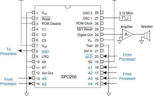
Figure 8.29 SP0256 speech synthesizer chip pinout
Figure 8.30 shows the speech synthesizer interfaced to the MIPS processor. The processor uses three memory-mapped I/O addresses to communicate with the speech synthesizer. We arbitrarily have chosen that the A6:1 port is mapped to address 0xFFFFFF00, ![]() to 0xFFFFFF04, and SBY to 0xFFFFFF08. Although the WriteData bus is 32 bits, only the least significant 6 bits are used for A6:1, and the least significant bit is used for
to 0xFFFFFF04, and SBY to 0xFFFFFF08. Although the WriteData bus is 32 bits, only the least significant 6 bits are used for A6:1, and the least significant bit is used for ![]() ; the other bits are ignored. Similarly, SBY is read on the least significant bit of the ReadData bus; the other bits are 0.
; the other bits are ignored. Similarly, SBY is read on the least significant bit of the ReadData bus; the other bits are 0.
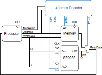
Figure 8.30 Hardware for driving the SP0256 speech synthesizer
Speech Synthesizer Device Driver
The device driver controls the speech synthesizer by sending an appropriate series of allophones over the memory-mapped I/O interface. It follows the protocol expected by the SPO256 chip, given below:
This sequence can be repeated for any number of allophones. The MIPS assembly in Code Example 8.1 writes five allophones to the speech chip. The allophone encodings are stored as 32-bit values in a five-entry array starting at memory address 0x10000000.
Code Example 8.1 SPEECH CHIP DEVICE DRIVER
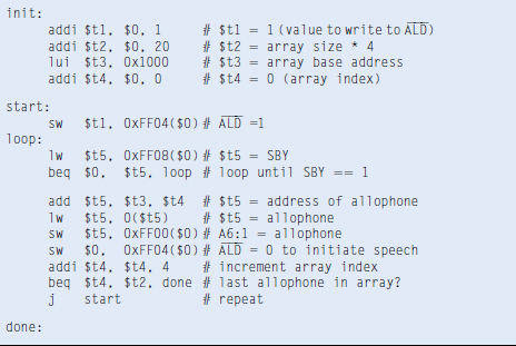
The assembly code in Code Example 8.1 polls, or repeatedly checks, the SBY signal to determine when the speech chip is ready to receive a new allophone. The code functions correctly but wastes valuable processor cycles that could be used to perform useful work. Instead of polling, the processor could use an interrupt connected to SBY. When SBY rises, the processor stops what it is doing and jumps to code that handles the interrupt. In the case of the speech synthesizer, the interrupt handler would send the next allophone, then let the processor resume what it was doing before the interrupt. As described in Section 6.7.2, the processor handles interrupts like any other exception.
8.6 REAL-WORLD PERSPECTIVE: IA-32 MEMORY AND I/O SYSTEMS*
As processors get faster, they need ever more elaborate memory hierarchies to keep a steady supply of data and instructions flowing. This section describes the memory systems of IA-32 processors to illustrate the progression. Section 7.9 contained photographs of the processors, highlighting the on-chip caches. IA-32 also has an unusual programmed I/O system that differs from the more common memory-mapped I/O.
8.6.1 IA-32 Cache Systems
The 80386, initially produced in 1985, operated at 16 MHz. It lacked a cache, so it directly accessed main memory for all instructions and data. Depending on the speed of the memory, the processor might get an immediate response, or it might have to pause for one or more cycles for the memory to react. These cycles are called wait states, and they increase the CPI of the processor. Microprocessor clock frequencies have increased by at least 25% per year since then, whereas memory latency has scarcely diminished. The delay from when the processor sends an address to main memory until the memory returns the data can now exceed 100 processor clock cycles. Therefore, caches with a low miss rate are essential to good performance. Table 8.5 summarizes the evolution of cache systems on Intel IA-32 processors.
The 80486 introduced a unified write-through cache to hold both instructions and data. Most high-performance computer systems also provided a larger second-level cache on the motherboard using commercially available SRAM chips that were substantially faster than main memory.
The Pentium processor introduced separate instruction and data caches to avoid contention during simultaneous requests for data and instructions. The caches used a write-back policy, reducing the communication with main memory. Again, a larger second-level cache (typically 256–512 KB) was usually offered on the motherboard.
The P6 series of processors (Pentium Pro, Pentium II, and Pentium III) were designed for much higher clock frequencies. The second-level cache on the motherboard could not keep up, so it was moved closer to the processor to improve its latency and throughput. The Pentium Pro was packaged in a multichip module (MCM) containing both the processor chip and a second-level cache chip, as shown in Figure 8.31. Like the Pentium, the processor had separate 8-KB level 1 instruction and data caches. However, these caches were nonblocking, so that the out-of-order processor could continue executing subsequent cache accesses even if the cache missed a particular access and had to fetch data from main memory. The second-level cache was 256 KB, 512 KB, or 1 MB in size and could operate at the same speed as the processor. Unfortunately, the MCM packaging proved too expensive for high-volume manufacturing. Therefore, the Pentium II was sold in a lower-cost cartridge containing the processor and the second-level cache. The level 1 caches were doubled in size to compensate for the fact that the second-level cache operated at half the processor’s speed. The Pentium III integrated a full-speed second-level cache directly onto the same chip as the processor. A cache on the same chip can operate at better latency and throughput, so it is substantially more effective than an off-chip cache of the same size.
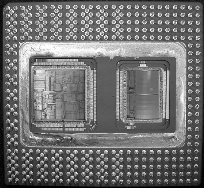
Figure 8.31 Pentium Pro multichip module with processor (left) and 256-KB cache (right) in a pin grid array (PGA) package (Courtesy Intel.)
Table 8.5 Evolution of Intel IA-32 microprocessor memory systems
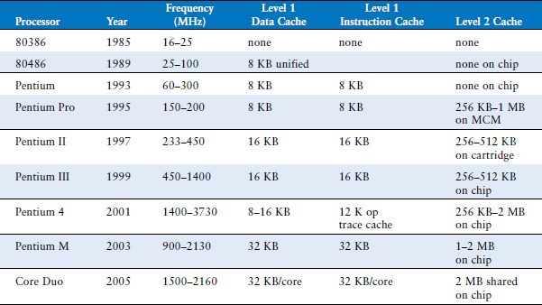
The Pentium 4 offered a nonblocking level 1 data cache. It switched to a trace cache to store instructions after they had been decoded into micro-ops, avoiding the delay of redecoding each time instructions were fetched from the cache.
The Pentium M design was adapted from the Pentium III. It further increased the level 1 caches to 32 KB each and featured a 1- to 2-MB level 2 cache. The Core Duo contains two modified Pentium M processors and a shared 2-MB cache on one chip. The shared cache is used for communication between the processors: one can write data to the cache, and the other can read it.
8.6.2 IA-32 Virtual Memory
IA-32 processors operate in either real mode or protected mode. Real mode is backward compatible with the original 8086. It only uses 20 bits of addresses, limiting memory to 1 MB, and it does not allow virtual memory.
Protected mode was introduced with the 80286 and extended to 32-bit addresses with the 80386. It supports virtual memory with 4-KB pages. It also provides memory protection so that one program cannot access the pages belonging to other programs. Hence, a buggy or malicious program cannot crash or corrupt other programs. All modern operating systems now use protected mode.
A 32-bit address permits up to 4 GB of memory. Processors since the Pentium Pro have bumped the memory capacity to 64 GB using a technique called physical address extension. Each process uses 32-bit addresses. The virtual memory system maps these addresses onto a larger 36-bit virtual memory space. It uses different page tables for each process, so that each process can have its own address space of up to 4 GB.
Although memory protection became available in the hardware in the early 1980s, Microsoft Windows took almost 15 years to take advantage of the feature and prevent bad programs from crashing the entire computer. Until the release of Windows 2000, consumer versions of Windows were notoriously unstable. The lag between hardware features and software support can be extremely long.
8.6.3 IA-32 Programmed I/O
Most architectures use memory-mapped I/O, described in Section 8.5, in which programs access I/O devices by reading and writing memory locations. IA-32 uses programmed I/O, in which special IN and OUT instructions are used to read and write I/O devices. IA-32 defines 216 I/O ports. The IN instruction reads one, two, or four bytes from the port specified by DX into AL, AX, or EAX. OUT is similar, but writes the port.
Connecting a peripheral device to a programmed I/O system is similar to connecting it to a memory-mapped system. When accessing an I/O port, the processor sends the port number rather than the memory address on the 16 least significant bits of the address bus. The device reads or writes data from the data bus. The major difference is that the processor also produces an M/![]() signal. When M/
signal. When M/![]() = 1, the processor is accessing memory. When it is 0, the process is accessing one of the I/O devices. The address decoder must also look at M/
= 1, the processor is accessing memory. When it is 0, the process is accessing one of the I/O devices. The address decoder must also look at M/![]() to generate the appropriate enables for main memory and for the I/O devices. I/O devices can also send interrupts to the processor to indicate that they are ready to communicate.
to generate the appropriate enables for main memory and for the I/O devices. I/O devices can also send interrupts to the processor to indicate that they are ready to communicate.
8.7 SUMMARY
Memory system organization is a major factor in determining computer performance. Different memory technologies, such as DRAM, SRAM, and hard disks, offer trade-offs in capacity, speed, and cost. This chapter introduced cache and virtual memory organizations that use a hierarchy of memories to approximate an ideal large, fast, inexpensive memory. Main memory is typically built from DRAM, which is significantly slower than the processor. A cache reduces access time by keeping commonly used data in fast SRAM. Virtual memory increases the memory capacity by using a hard disk to store data that does not fit in the main memory. Caches and virtual memory add complexity and hardware to a computer system, but the benefits usually outweigh the costs. All modern personal computers use caches and virtual memory. Most processors also use the memory interface to communicate with I/O devices. This is called memory-mapped I/O. Programs use load and store operations to access the I/O devices.
EPILOGUE
This chapter brings us to the end of our journey together into the realm of digital systems. We hope this book has conveyed the beauty and thrill of the art as well as the engineering knowledge. You have learned to design combinational and sequential logic using schematics and hardware description languages. You are familiar with larger building blocks such as multiplexers, ALUs, and memories. Computers are one of the most fascinating applications of digital systems. You have learned how to program a MIPS processor in its native assembly language and how to build the processor and memory system using digital building blocks. Throughout, you have seen the application of abstraction, discipline, hierarchy, modularity, and regularity. With these techniques, we have pieced together the puzzle of a microprocessor’s inner workings. From cell phones to digital television to Mars rovers to medical imaging systems, our world is an increasingly digital place.
Imagine what Faustian bargain Charles Babbage would have made to take a similar journey a century and a half ago. He merely aspired to calculate mathematical tables with mechanical precision. Today’s digital systems are yesterday’s science fiction. Might Dick Tracy have listened to iTunes on his cell phone? Would Jules Verne have launched a constellation of global positioning satellites into space? Could Hippocrates have cured illness using high-resolution digital images of the brain? But at the same time, George Orwell’s nightmare of ubiquitous government surveillance becomes closer to reality each day. And rogue states develop nuclear weapons using laptop computers more powerful than the room-sized supercomputers that simulated Cold War bombs. The microprocessor revolution continues to accelerate. The changes in the coming decades will surpass those of the past. You now have the tools to design and build these new systems that will shape our future. With your newfound power comes profound responsibility. We hope that you will use it, not just for fun and riches, but also for the benefit of humanity.
Exercises
Exercise 8.1 In less than one page, describe four everyday activities that exhibit temporal or spatial locality. List two activities for each type of locality, and be specific.
Exercise 8.2 In one paragraph, describe two short computer applications that exhibit temporal and/or spatial locality. Describe how. Be specific.
Exercise 8.3 Come up with a sequence of addresses for which a direct mapped cache with a size (capacity) of 16 words and block size of 4 words outperforms a fully associative cache with least recently used (LRU) replacement that has the same capacity and block size.
Exercise 8.4 Repeat Exercise 8.3 for the case when the fully associative cache outperforms the direct mapped cache.
Exercise 8.5 Describe the trade-offs of increasing each of the following cache parameters while keeping the others the same:
Exercise 8.6 Is the miss rate of a two-way set associative cache always, usually, occasionally, or never better than that of a direct mapped cache of the same capacity and block size? Explain.
Exercise 8.7 Each of the following statements pertains to the miss rate of caches. Mark each statement as true or false. Briefly explain your reasoning; present a counterexample if the statement is false.
Exercise 8.8 A cache has the following parameters: b, block size given in numbers of words; S, number of sets; N, number of ways; and A, number of address bits.
Exercise 8.9 A 16-word cache has the parameters given in Exercise 8.8. Consider the following repeating sequence of lw addresses (given in hexadecimal):
40 44 48 4C 70 74 78 7C 80 84 88 8C 90 94 98 9C 0 4 8 C 10 14 18 1C 20
Assuming least recently used (LRU) replacement for associative caches, determine the effective miss rate if the sequence is input to the following caches, ignoring startup effects (i.e., compulsory misses).
Exercise 8.10 Suppose you are running a program with the following data access pattern. The pattern is executed only once.
0x0, 0x8, 0x10, 0x18, 0x20, 0x28
Exercise 8.11 You are building an instruction cache for a MIPS processor. It has a total capacity of 4C = 2c+2 bytes. It is N = 2n-way set associative (N ≥ 8), with a block size of b = 2b’ bytes (b ≥ 8). Give your answers to the following questions in terms of these parameters.
Exercise 8.12 Consider a cache with the following parameters:
N (associativity) = 2, b (block size) = 2 words, W (word size) = 32 bits, C (cache size) = 32 K words, A (address size) = 32 bits. You need consider only word addresses.
Figure 8.32 Building blocks
Exercise 8.13 You’ve joined a hot new Internet startup to build wrist watches with a built-in pager and Web browser. It uses an embedded processor with a multilevel cache scheme depicted in Figure 8.33. The processor includes a small on-chip cache in addition to a large off-chip second-level cache. (Yes, the watch weighs 3 pounds, but you should see it surf!)
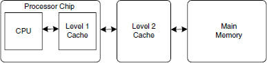
Figure 8.33 Computer system
Assume that the processor uses 32-bit physical addresses but accesses data only on word boundaries. The caches have the characteristics given in Table 8.6. The DRAM has an access time of tm and a size of 512 MB.
Table 8.6 Memory characteristics
| Characteristic | On-chip Cache | Off-chip Cache |
|---|---|---|
| organization | four-way set associative | direct mapped |
| hit rate | A | B |
| access time | ta | tb |
| block size | 16 bytes | 16 bytes |
| number of blocks | 512 | 256K |
Exercise 8.14 This chapter described the least recently used (LRU) replacement policy for multiway associative caches. Other, less common, replacement policies include first-in-first-out (FIFO) and random policies. FIFO replacement evicts the block that has been there the longest, regardless of how recently it was accessed. Random replacement randomly picks a block to evict.
Exercise 8.15 You are building a computer with a hierarchical memory system that consists of separate instruction and data caches followed by main memory. You are using the MIPS multicycle processor from Figure 7.41 running at 1 GHz.
Exercise 8.16 If a computer uses 64-bit virtual addresses, how much virtual memory can it access? Note that 240 bytes = 1 terabyte, 250 bytes = 1 petabyte, and 260 bytes = 1 exabyte.
Exercise 8.17 A supercomputer designer chooses to spend $1 million on DRAM and the same amount on hard disks for virtual memory. Using the prices from Figure 8.4, how much physical and virtual memory will the computer have? How many bits of physical and virtual addresses are necessary to access this memory?
Exercise 8.18 Consider a virtual memory system that can address a total of 232 bytes. You have unlimited hard disk space, but are limited to only 8 MB of semiconductor (physical) memory. Assume that virtual and physical pages are each 4 KB in size.
Exercise 8.19 You decide to speed up the virtual memory system of Exercise 8.18 by using a translation lookaside buffer (TLB). Suppose your memory system has the characteristics shown in Table 8.7. The TLB and cache miss rates indicate how often the requested entry is not found. The main memory miss rate indicates how often page faults occur.
Table 8.7 Memory characteristics
| Memory Unit | Access Time (Cycles) | Miss Rate |
|---|---|---|
| TLB | 1 | 0.05% |
| cache | 1 | 2% |
| main memory | 100 | 0.0003% |
| disk | 1,000,000 | 0% |
Exercise 8.20 Suppose the MIPS multicycle processor described in Section 7.4 uses a virtual memory system.
Exercise 8.21 The virtual memory system you are designing uses a single-level page table built from dedicated hardware (SRAM and associated logic). It supports 25-bit virtual addresses, 22-bit physical addresses, and 216-byte (64 KB) pages. Each page table entry contains a physical page number, a valid bit (V) and a dirty bit (D).
Exercise 8.22 Describe a scenario in which the virtual memory system might affect how an application is written. Be sure to include a discussion of how the page size and physical memory size affect the performance of the application.
Exercise 8.23 Suppose you own a personal computer (PC) that uses 32-bit virtual addresses.
Exercise 8.24 Use MIPS memory-mapped I/O to interact with a user. Each time the user presses a button, a pattern of your choice displays on five light-emitting diodes (LEDs). Suppose the input button is mapped to address 0xFFFFFF10 and the LEDs are mapped to address 0xFFFFFF14. When the button is pushed, its output is 1; otherwise it is 0.
Exercise 8.25 Finite state machines (FSMs), like the ones you built in Chapter 3, can also be implemented in software.
Interview Questions
The following exercises present questions that have been asked on interviews.
Question 8.1 Explain the difference between direct mapped, set associative, and fully associative caches. For each cache type, describe an application for which that cache type will perform better than the other two.
Question 8.2 Explain how virtual memory systems work.
Question 8.3 Explain the advantages and disadvantages of using a virtual memory system.
Question 8.4 Explain how cache performance might be affected by the virtual page size of a memory system.
Question 8.5 Can addresses used for memory-mapped I/O be cached? Explain why or why not.
1 We realize that library usage is plummeting among college students because of the Internet. But we also believe that libraries contain vast troves of hard-won human knowledge that are not electronically available. We hope that Web searching does not completely displace the art of library research.
2 Recall that the 16-bit immediate 0xFFF4 is sign-extended to the 32-bit value 0xFFFFFFF4.
3 Data from Patterson and Hennessy, Computer Organization and Design, 3rd Edition, Morgan Kaufmann, 2005. Used with permission.