Even though it is still early in our study of simulation, we now have the tools required to use simulation effectively to investigate the design and operating characteristics of a number of important systems. While there are many candidate systems that could be explored at this point in our studies, our focus in this chapter is on the phase-locked loop (PLL). There are a variety of justifications for this choice. First, the PLL is a basic building block for many subsystems used in the implementation of modern communication systems. PLLs are widely used in frequency synthesis, for frequency multipliers and dividers, for carrier and symbol synchronization, and in the implementation of coherent receivers [1, 2]. There are many other applications for the PLL. Since the PLL is a nonlinear system, and is therefore very difficult to analyze and design using traditional (nonsimulation based) methods, simulation is widely used for the design and analysis of systems based on the PLL. We will see that a basic knowledge of numerical integration methods, such as we gained in the preceding chapter, provides the concepts necessary to develop effective simulations for PLLs and for many other systems of interest.
Another reason for using the PLL for a detailed example simulation is that the PLL involves feedback. We will see that systems involving feedback must be simulated with care, especially with respect to the sampling frequency, if significant simulation errors are to be avoided.
As discussed in Chapter 4, analysis based on lowpass system models is equivalent to an analysis based on the corresponding bandpass system models, assuming of course that the lowpass models are correctly developed. In addition, simulation models derived from lowpass analytical models execute much more quickly than simulations based on bandpass models. Thus, much of the work in this chapter will be based on lowpass models. Finally, all simulations presented in this chapter are deterministic simulations, as discussed in Chapter 1.
Although the focus of this chapter is to illustrate a number of elementary simulation techniques, and we use the PLL only as an interesting case study relevant to the study of communications, sufficient theory is presented to make the results understandable and to provide a “sanity check” on the simulation results. It is important, as discussed in Chapter 1, that analysis and simulation work hand in hand. This chapter, therefore, begins with a basic description of the PLL. Using the first-order loop as an example, we show how the loop achieves phase lock. Attention is then turned to the second-order loop, which is more useful in system implementations. We use simulation to illustrate the cycle-slipping phenomena and to determine the time required to achieve phase lock. Simulation is accomplished by developing a discrete-time simulation model for the PLL by replacing continuous-time integration by the trapezoidal integration rule explored in the previous chapter.
Later in this chapter we will appreciate that, in addition to having the tools for studying PLLs, we also have the required tools for using simulation to study any system that can be defined in terms of a differential equation. The differential equation, and therefore the underlying system, can be nonlinear, time-varying, or both nonlinear and time-varying. Thus, upon completing this chapter, we will have the tools required to simulate a wide variety of extremely complicated systems.
The basic model of a PLL is illustrated in Figure 6.1. The input signal is assumed to be
and the signal at the output of the voltage-controlled oscillator (VCO) is assumed to have the form
The basic role of a PLL is to synchronize the phase of the VCO with the phase of the input signal so that the phase error, φ(t) = θ(t), is small. We will see how this is accomplished in the following sections.
PLLs typically operate in one of two modes, acquisition and tracking. In the acquisition mode, the PLL is attempting to synchronize, in both frequency and phase, the VCO output with an input signal. We will see that, in the acquisition mode, phase errors can be quite large. In this case, PLL operation is distinctly nonlinear, and a nonlinear model is required for analysis. Analysis of nonlinear models is extremely difficult and simulation is often required. In the tracking mode, however, the phase error is often small for long periods of time, and analysis using a simple linear model can often provide satisfactory results without the need for simulation. The standard loop parameters, as we will see, are defined in terms of the linear model. Thus, we have interest in both linear and nonlinear models. The focus of the simulations developed in this chapter will be on the nonlinear behavior of the system.
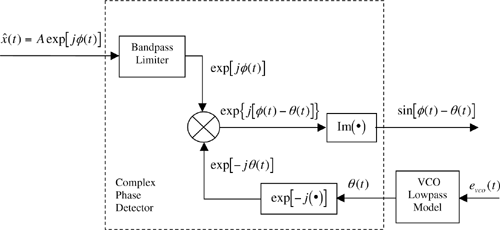
The first step in the development of a simulation model for a PLL is to model the phase detector. The characteristics of the phase detector determine, in large part, the operating characteristics of the PLL. There are many different types of phase detectors, and the choice of the phase detector model to be used in a given situation is dependent upon the application. The most common phase detector model, referred to as the sinusoidal phase detector, is one in which the output of the phase detector is proportional to the sine of the phase error. The sinusoidal phase detector can be viewed as consisting of a multiplier and a lowpass filter as shown in Figure 6.2. The only function of the lowpass filter is to remove the second harmonic of the carrier frequency resulting from the multiplication. We will see later that, in practical applications, the lowpass filter is not necessary.
Using the phase-detector model shown in Figure 6.2, the output of the phase detector is
where the quantity φ(t) − θ(t) is referred to as the phase error. Later we will denote the phase error by ψ(t), but for now it is better to keep all of our expressions in terms of input phase, φ(t), and VCO phase, θ(t). We desire the VCO phase to be an estimator of the input phase and therefore proper operation of the PLL requires that the phase error be driven toward zero. The steady-state phase error may or may not be zero depending upon the characteristics of the input signal and the loop filter.
Note that the PLL input and the VCO output are in phase quadrature for φ(t) = θ(t). This is required if the phase detector output is to be an odd function of the phase error. It is easily seen that if cosine functions are used in both (6.1) and (6.2), with the arguments unchanged, the phase detector output will be proportional to cos [φ(t) − θ(t)], which is an even function of the phase error. This, of course, yields the undesirable situation in which negative phase errors are not distinguishable from positive phase errors.
After multiplication by the loop amplifier gain, µ, the phase detector output ed(t) is filtered by a loop filter having the transfer function F(s) and unit impulse response f(t). The input to the VCO is therefore given by
which is simply the convolution of the loop filter impulse response with the loop filter input. For a sinusoidal phase detector this becomes
The next step is to relate the VCO phase deviation θ(t) to the VCO input. By definition, the frequency deviation of the VCO output is proportional to the VCO input signal so that
where Kd is the VCO constant and has units of Hz/v. Solving for θ(t) gives
Substituting (6.5) for evco(t) yields
where G is defined as the loop gain and is given by
Equation (6.8) is the nonlinear integral equation relating the phase deviation of the input φ(t) to the VCO phase deviation θ(t). Keep in mind that the impulse response of the loop filter, f(t), is still arbitrary.
In developing system simulations, one should be careful about combining parameters as we did in (6.9). Combining terms is a valid step if the purpose of the simulation is to determine the input-output characteristics of the system or the characteristics of the system as a whole, such as the time required for a PLL to achieve phase lock. On the other hand, if the simulation is being performed to examine the waveforms present at the input or the output of various functional blocks within the system, the parameters that define G cannot be grouped together. It they are grouped together, the waveforms present at various points in the system will not be scaled properly or may not even be identifiable.
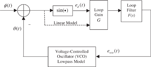
It is apparent from (6.8) that the relationship between θ(t) and φ(t) does not depend in any way on the carrier frequency fc, and therefore the carrier frequency need not be considered in the simulation model. We therefore seek a model that establishes the proper relationship between θ(t) and φ(t) without consideration of the carrier frequency. This model is shown in Figure 6.3 and is known as the nonlinear phase model of the PLL. It is a nonlinear model because of the sinusoidal nonlinearity and is a phase model because the model establishes the relationship between the input phase deviation and the VCO phase deviation rather than establishing the relationship between the actual loop input and VCO output signals as expressed by (6.1) and (6.2), respectively. It is important to remember that the input to the model illustrated in Figure 6.1 is the actual bandpass signal present in the system under study, while the input to the nonlinear phase model shown in Figure 6.3 is the phase deviation of the input bandpass signal. If the phase deviation of the input signal, φ(t), the carrier frequency, and the signal amplitude are known, (6.1) is completely determined. In like manner, if the VCO phase deviation, θ(t), the carrier frequency, and the signal amplitude are known, the VCO output expressed by (6.2) is completely determined. Thus, the nonlinear phase model expresses the relationship between the input phase and the VCO phase, which are the important quantities of interest. In simulation applications the nonlinear phase model pays additional dividends. Since the loop input and VCO output phase deviations are lowpass signals, they can be sampled at a much lower sampling rate than the signals expressed by (6.1) and (6.2), which are bandpass signals.
At this point another word is in order concerning the lowpass filter used to remove the second harmonic of the carrier produced by the multiplier present in the phase detector model. This filter is simply part of a conceptual model and, as mentioned previously, need not be present in the physical device. It is easily seen that this filter may be eliminated. Equation (6.7) shows that the VCO model is simply an integrator. Since an integrator is a lowpass filter, which has infinite gain at f = 0 and unity gain at f = 1/(2π) Hz, the VCO will prevent the second harmonic of the carrier frequency from propagating around the loop and appearing at the VCO output.
Example 6.1.
In this example a general technique for modeling phase detectors is examined. Although a sinusoidal phase detector is assumed throughout this chapter, it is easy to model a phase detector having an arbitrary characteristic. A general technique is to represent the function relating the output of the phase detector to the input of the phase detector by a Fourier series. This gives
where ck represents the Fourier coefficients of the phase detector characteristic and ψ(t) = φ(t) − θ(t) is the phase error. A given phase detector characteristic can be modeled to any required accuracy by adjusting the number of terms, N, used in the series expansion. Note that only odd terms are included in the series so that ed(t) will be an odd function of the phase error. As a simple example, the sinusoidal phase detector defined in Figure 6.2 is represented by
where N ≥ 1.
The MATLAB code for the phase detector described by (6.10) is easily written in vector form. The vector B is defined as
B = [1 2 3 ... N]
and the vector of Fourier coefficients is
C = [c1 c2 c3 ... cN]
Assuming that pdin and pdout are the input and output of the phase detector model, respectively, the phase detector output can be written
pdout= (sin(B*pdin)) *C’
where C’ is the transpose of C. Since B and C are completely defined by the phase detector model, they are fixed and should be defined outside of the simulation loop.
We will later see that the most general method for simulating systems is to use the Monte Carlo technique, which requires that the simulation loop be executed a large number of times. When the Monte Carlo technique is used, very long simulation run times often result and it becomes important to use the most efficient algorithms possible. A vector formulation is therefore used to compute pdout in order to avoid the looping operation typically used to evaluate summations.
Phase-locked loops are usually modeled so that the loop input is the phase deviation φ(t). When the PLL is used within a system, one often wishes to develop a model in which the loop input is a complex envelope lowpass signal A exp [jφ(t)] representing (6.1). Such a model is illustrated in Figure 6.4 for a sinusoidal phase detector. Phase detectors having other characteristics are easily derived.
As illustrated in Figure 6.4 the input signal, in complex envelope form, is first passed through a bandpass limiter, which was discussed in Chapter 4, Example 4.10. (Here we assume that the parameter B, defined in Example 4.1, is set equal to one.)[1] The operation of the complex phase detector model should be clear from the expressions given in Figure 6.4 defining the signal at each point in the model. Note that the inputs to the multiplier are expressed in complex exponential form and that the imaginary part of the multiplier output gives sin [φ(t) − θ(t)].
If the phase error is small so that the linear approximation
can be made, the loop equation, (6.8), becomes
This results in the linear phase model of the PLL, which is identical to the nonlinear phase model except that the sinusoidal nonlinearity is removed. This is shown by the dotted line in Figure 6.3.
Taking the Laplace transform of (6.13), recognizing that integration is equivalent to division by s and that convolution in the time domain is equivalent to multiplication in the frequency domain, yields
The transfer function H (s) relating the VCO phase to the input phase is therefore given by
It must be kept in mind that the transfer function given in (6.15) is based on a linear assumption and, in general, is not valid. Strictly speaking, transfer functions for nonlinear systems do not exist.
Even though simulation is typically used to study the nonlinear behavior of the PLL, linear models are useful for several purposes. First, as we will see in a following section, loop parameters are almost always defined in terms of the linear model. In addition, analytical analysis based on the linear model is usually easy and can often help verify (sanity check) the simulation results. Finally, linear models are often used to study tracking behavior for those applications in which the signal being tracked is varying at a rate slower than the loop bandwidth.
The acquisition and tracking behavior of a PLL depends in large measure upon the order of the loop, and for this reason we consider two choices for the loop filter transfer function. The order of a PLL implementation is equal to the number of finite poles in the transfer function H(s) as given by (6.15). It follows that the order of a given PLL implementation exceeds the number of poles of F(s) by one, with the extra pole resulting from the integration in the VCO model. We now briefly look at first-order (no loop filter) and second-order PLLs (first-order loop filter). Although the first-order PLL does not have desirable operating characteristics, as will be shown, we will use the first-order PLL to illustrate the mechanism by which the loop achieves phase lock.
For the first-order PLL F(s) = 1 so that
Substitution into (6.8) yields
Performing the integration on λ using the sifting property of the impulse (delta) function gives
Differentiating with respect to t yields the differential equation
Writing (6.19) in terms of the phase error ψ(t) = φ(t) − θ(t) provides the differential equation relating the phase error and the input phase. This is
We now determine the phase error for an input frequency step.
In order to study the response of a first-order PLL to a step in frequency of fΔ Hz at time t0 we let
so that (6.20), for t > t0, becomes
This gives the relationship between the frequency error and the phase error for t > t0.
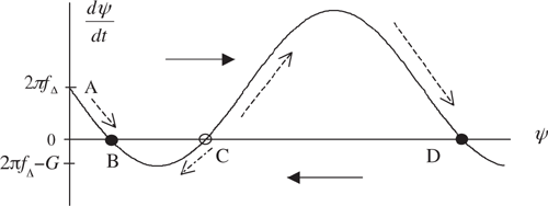
Equation (6.22) is illustrated in Figure 6.5 and is called the phase plane equation or, simply, the phase plane, and describes the dynamic behavior of the system. The phase plane has a number of important properties, and understanding a few of them provides insight into how, and under what conditions, the loop achieves lock. Note that the relationship between phase error and frequency error must satisfy (6.22) at each point in time. These time-dependent points are known as operating points. In the upper-half phase plane, the operating point moves from left to right and in the lower-half phase plane the operating point moves from right to left. This is easily seen. First we let
where Δψ and Δt denote small increments in phase error and time, respectively. Clearly Δt > 0 for all t, since time always increases. Thus, dψ > 0 in the upper-half phase plane and dψ < 0 in the lower-half phase plane. The phase error therefore increases (moves from left to right) in the upper-half phase plane and the phase error decreases (moves from right to left) in the lower-half phase plane. This is illustrated by the solid arrows in Figure 6.5. A stationary operating point can lie only on the boundary between the upper-half phase plane and the lower-half phase plane. This, of course, denotes that the phase error is constant or, equivalently, that the frequency error is zero. An operating point is stable if, after a small perturbation, the operating point returns to its original location. If a small perturbation results in the operating point moving to a new position, the original operating point is called unstable. Thus points B and D in Figure 6.5 are stable operating points and point C is an unstable operating point. Movement of the operating points is indicated by the dotted lines in Figure 6.5.
It can be seen from (6.22) that if 2πfΔ < G, the steady-state operating point is the stable point B given that the initial operating point due to the frequency step is A. At this point the frequency error is zero and the steady-state phase error is the solution of (6.22) with dψ/dt = 0. This gives the steady-state phase error
As a final observation of the phase plane, note that if 2πfΔ > G there is no solution to (6.22) for zero frequency error dψ/dt and the operating point will move to the right for all time for fΔ > 0 and will move to the left for all time for fΔ < 0. The loop gain G therefore becomes the lock range for the first-order loop. Note from (6.15) that G is also the loop bandwidth (in rad/s) for the first-order PLL.
Example 6.2.
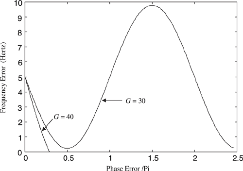
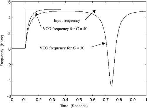
As a simple example suppose that fΔ = 5 so that 2πfΔ = 31.42. Also assume that the loop gain takes on two different values, namely, G = 30 and G = 40. The resulting phase planes are shown in Figure 6.6. The phase plane shows that for fΔ = 5, G = 40, and 2πfΔ < G, the frequency error decreases to zero monotonically. There is no overshoot, since the system is first order. For fΔ = 5 and G = 30, 2πfΔ > G, and (6.22) has no solution for zero frequency error. For this case phase lock will not be achieved and the system will forever oscillate.
The phase plane is made clearer by Figure 6.7, which shows the input frequency deviation, dφ/dt, and the VCO frequency deviation, dθ/dt, for G = 30 and G = 40. The resulting input frequency deviation and VCO frequency deviation are shown in Figure 6.7 for 2πfΔ = 31.42 with G = 30 and G = 40. Note that for G = 40 the loop achieves phase lock while for G = 30 phase lock is not achieved and the VCO phase deviation oscillates forever.
We have seen that both the lock range of the first-order PLL and the loop bandwidth are determined by the parameter G. For most applications a large lock range and a small loop bandwidth are desired. This cannot be acccomplished with a first-order loop and, therefore, the first-order PLL is not usually practical. The second-order loop is a practical system for many applications and will provide aninteresting simulation case study.
We saw in the preceding section that the first-order PLL has a limited lock range. In addition, since the loop has only a single parameter, the ability to adjust loop parameters to meet a given set of operating specifications is severely limited. Improved operating characteristics and design capabilities are achieved by changing the loop filter so that a second-order PLL results.
The general form of the loop filter for a second-order PLL is
The perfect second-order PLL is defined by λ = 0, which denotes a loop filter containing a perfect integration (pole at s = 0). In typical applications, λ ≪ 1. Substituting the loop filter transfer function into (6.15) gives
for the loop linear-model transfer function.
Linear second-order systems are usually parameterized in terms of the system damping factor, denoted ζ, and the system natural frequency, denoted ωn. The denominator of the transfer function is often referred to as the characteristic polynomial, which, for a second-order system, is expressed in the standard form
Equating the characteristic polynimial in (6.26) to the standard form yields
In typical applications the PLL is designed for a given damping factor and natural frequency by specifying ζ and ωn. The required physical parameters (in this case G and a) are then determined so that the design values of ζ and ωn are achieved. Equating terms having like powers of s in (6.27) gives
and
Assuming that λ is a known constant, we may solve (6.29) for a and substitute the result in (6.28). This gives the quadratic equation
which, upon solving for G yields
This result, together with (6.29) gives
Note that since a is a real parameter, λ must be less than ζ2. Typical values of ζ2 lie in the neighborhood of 1/2 (![]() is a common choice) and, as previously mentioned, λ ≪ 1. Note that for a perfect second-order PLL, G = 2ζωn and a = ωn/2ζ.
is a common choice) and, as previously mentioned, λ ≪ 1. Note that for a perfect second-order PLL, G = 2ζωn and a = ωn/2ζ.
We are now in a position to simulate a second-order PLL and use our very basic knowledge of PLL theory to sanity check the results. First, however, we pause to consider a simple architecture for the overall simulation program. The simulation model is then developed and the simulation is executed. Finally, the error sources in the simulation are briefly discussed.
It is often useful to divide the software for a simulation into several distinct programs as shown in Figure 6.8. Here we see three separate elements of the overall simulation program. These elements are designated the preprocessor, the simulation engine, and the postprocessor. These three programs perform three distinctly different functions and, if desired, can be developed in three different languages. Partitioning a simulation in this manner results in simulation code that is more easily developed, understood, and maintained. It is also efficient, since code segments can often be reused in different applications. This is especially true of the postprocessor.
The purpose of the preprocessor is to specify all parameters necessary to define the system under study (system parameters) and to set the parameters that manage execution of the simulation (intrinsic parameters). Example system parameters include items such as filter orders, filter types and bandwidths, amplifier gains, code rate, spreading ratios, carrier frequencies, bit rates, and signal-to-noise ratios. Intrinsic parameters include the sampling frequency, settle times (required to ensure that startup transients have decayed to negligible values), and the number of samples to be processed. In addition, the data to be passed to the postprocessor for analysis or plotting must be saved by the simulation and, therefore, the data files required by the postprocessor must be specified by the preprocessor so that the appropriate data is saved as the simulation is executed. An example might be a vector of waveform samples and a vector of sample times used in the postprocessor to calibrate the time axis of signal plots. Once all of the necessary information has been specified in the preprocessor, the data created within the preprocessor is typically written to a file so that it is available to the simulation engine and to the postprocessor. In the MATLAB examples to follow, the preprocessor data is written to the MATLAB workspace.
The simulation engine reads the data stored in the file (or in the workspace) created by the preprocessor and executes the simulation. The purpose of a simulation is, of course, to generate data for later investigation using the postprocessor. This may take the form of numbers (signal-to-noise ratios, bit error rates, code gain, etc.) or may be vectors of sample values for additional processing by the postprocessor. The information generated by the simulation engine is stored in files and passed to the postprocessor. In the case of MATLAB it is usually most convenient to simply leave the data generated by the simulation engine in the MATLAB workspace.
The postprocessor takes the data generated by the simulation engine and generates the final simulation products required by the user. These may include waveform plots, signal constellations, plots of the bit error rate as a function of Eb/N0, the power spectral density at a point in the system under study, eye diagrams, and histograms. The list of possibilities is almost endless. Appropriately derived graphical displays can greatly facilitate an understanding of the system under study. We consider postprocessing and the generation of graphical displays in more detail in Chapter 8.
The postprocessor clearly requires a significant level of graphical support. This was one reason to relay on MATLAB for the applications presented here. Postprocessors are most useful when they are menu driven and provide a variety of signal processing and display options. While the simulations to follow in this chapter are quite simple, as are the preprocessor and the postprocessor, they serve to demonstrate the roles of each of these elements of a simulation.
As previously mentioned, the preprocessor, the simulation engine, and the postprocessor can be written in different languages. A recent project by one of the authors used Visual Basic for the preprocessor, C++ for the simulation engine (chosen for execution speed), and MATLAB for the postprocessor. MATLAB is frequently chosen for postprocessor development because of MATLAB’s rich graphics library.
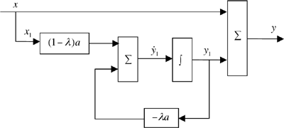
The simulation model is straightforward except, perhaps, for the loop filter. Since the loop filter transfer function, as defined by (6.25) is not a proper function,[2] long division is applied to yield
Thus, F(s) can be realized as a parallel combination of two transfer functions, the first of which is a constant and the second of which is F1(s). Clearly
where Y1(s) and X1(s) represent the Laplace transform of the output and input, respectively, of the subfilter F1(s). Cross-multiplying gives
which in the time domain is
It follows that the loop filter is realized by the system illustrated in Figure 6.9.
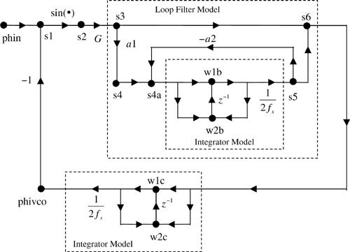
The next step in developing the simulation code for the second-order PLL is to develop a signal-flow graph[3] for the system and to designate the points on the signal-flow graph at which the signals are to be defined. The resulting signal-flow graph is illustrated in Figure 6.10. Note that the loop filter model follows directly from Figure 6.9 with
and
The points at which the signals are to be defined in the simulation code are represented by the heavy black dots on the signal-flow graph. Note that we are using trapezoidal integration as developed in the previous chapter.
The simulation code follows directly from the signal-flow graph. Each sample value computed in the simulation loop carries an identification corresponding to the identification defined in the signal-flow graph. For example, the line of code
s2 = sin(s1)
defines the sinusoidal nonlinearity representing the phase detector, where s1 and s2 are defined in the signal-flow graph. All other lines of code in the simulation loop follow in a similar manner. Thus, the MATLAB code that realizes the main simulation loop is
% beginning of simulation loop
for i=1:npts
    s1 = phin-phivco;               % phase error
    s2 = sin(s1);                   % sinusoidal phase detector
    s3 = G*s2;
    s4 = a1*s3;
    s4a = s4-a2*s5;                 % loop filter integrator input
    w1b = s4a+w2b;                  % filter integrator (step 1)
    w2b = s4a+w1b;                  % filter integrator (step 2)
    s5 = w1b/twofs;                 % generate filter output
    s6 = s3+s5;                     % VCO integrator input
    w1c = s6+w2c;                   % VCO integrator(step 1)
    w2c = s6+w1c;                   % VCO integrator(step 2)
    phivco = w1c/twofs;             % generate VCO output
end
% end of simulation loop
The constant twofs is twice the sampling frequency, as required for the trapezoidal integrator, and is computed outside of the simulation loop.
The complete simulation code for the second-order PLL is given in Appendix A. Note that the code given in Appendix A differs slightly from the code given here, since vectors are developed for the input phase, the phase error, and the VCO frequency. These vectors are required by the postprocessor for plotting waveforms. The MATLAB code for the preprocessor and the postprocessor are given in Appendices B and C, respectively. Note that the postprocessor is menu driven. Menu-driven postprocessors are typical in simulation packages.
An example simulation was performed assuming that the PLL input frequency deviation is a unit step at time t0. Thus:
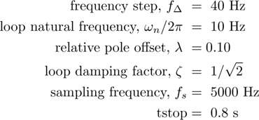
which is the same input that we assumed for the first-order PLL previously. The following PLL parameters are used:
These items are entered using the preprocessor.
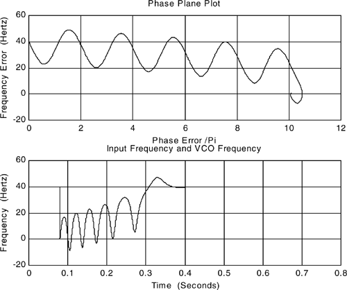
The menu selections used in the example postprocessor (Appendix C) allow the simulation user to examine a number of items of interest with ease. These include the input frequency and VCO frequency, the frequency error, and the phase plane. For space considerations we illustrate only two postprocessor-generated plots here. The phase plane is illustrated in the top pane of Figure 6.11. The input frequency (the unit step of 40 Hz at t0 = 0.08) and the VCO frequency (the waveform that oscillates) are illustrated in the bottom pane of Figure 6.11. It should be remembered that we are working with lowpass models. Thus, input frequency and VCO frequency actually refer to the input frequency deviation and the VCO frequency deviation from the nominal carrier frequency, fc.
Note from the phase plane that the five cycles are slipped and that the steady-state error is slightly greater than 10π. From Figure 6.11 we see that the input frequency steps by 40 Hz as specified. The VCO frequency, however, oscillates through five cycles and then phase lock is achieved on the sixth cycle. This behavior is referred to as “cycle slipping” and is characteristic of nonlinear synchronizers when the change in input frequency significantly exceeds the natural frequency.
There are a number of error sources present in this simulation. These error sources, as discussed in Chapter 1, result both from mapping the physical device to an analytical model and from mapping the analytical model to the simulation model. These error sources are briefly discussed in the following paragraphs.
In developing an analytical model for a device, a number of assumptions are often made. These approximations typically involve idealizations of the various loop components and may not be valid if highly accurate simulations of a physical device are to be obtained. Where highly accurate simulation results are required, laboratory measurements are often necessary to determine sufficiently accurate component models. Various restrictions may also apply to signals within the loop that are not accounted for in a basic analytical model. For example, in the simulation just developed, the signal levels at any point in the loop were allowed to rise to any value dictated by the loop equations. In practice, however, the maximum value of any signal in the loop will be constrained by the power supply voltages. Other approximations may also require consideration. Depending on the requirements of the simulation user, a more detailed analytical model than the one used here for a second-order PLL may be necessary.
There are a number of potential error sources associated with the process of mapping the analytical model to the simulation model. For example, while the physical system processes continuous-time signals, the simulation, of necessity, processes samples of continuous-time signals. Sampling, of course, leads to aliasing errors. In some cases quantizing errors must be considered. In addition, analog filters in the hardware or analytical model must be replaced by digital filters in the simulation model. As we previously saw, the digital filter never has the same amplitude and phase response as the analog filter it replaces. Errors resulting from frequency warping or aliasing must often be considered.
An important error source is present in all systems involving feedback. For example, the output of the phase detector in the analog (hardware) PLL is defined by
Ideally, a discrete-time model for this would be
where φ(nT) is the “current” input to the PLL. However, θ(nT), the phase deviation at the output of the VCO, is not available, since ed(nT) is needed to compute it. The computational “deadlock” resulting from the interdependency between ed(nT) and θ(nT) is handled by using the previously computed value of the VCO phase deviation, θ((n − 1)T), to compute ed(nT). In other words, the model defined by (6.42) is replaced by
Thus, a one-sample delay has been introduced in the feedback loop that is not present in the physical model or in the analytical model. While this one-sample delay may have a negligible effect on the accuracy of the simulation for small simulation step size (high sampling frequency), it may well have an effect for practical simulation step sizes. The effect of this one-sample delay is to induce a linear phase shift (a constant time delay) on the open-loop transfer function. This reduces the phase margin of the system and, if the simulation step size is sufficiently large, can drive the system into instability.
If a simulation is to have a given level of accuracy the simulation models must be based on analytical models having at least the same level of accuracy. If the physical devices being modeled exhibit significant variation across a group of similar devices, it is usually necessary to base the simulation models on measured data carefully obtained using accurately calibrated instrumentation. Nonlinear amplifiers often fall into this category, as do devices containing components that exhibit significant aging effects. Other examples are models for channels that exhibit significant multipath effects.
Only a few error sources have been considered here, but it is important to realize that, as discussed in Chapter 1, the analytical model captures only a portion of the characteristics (hopefully the most important characteristics) of the physical device, and additional errors are incurred as the analytical model is mapped to a simulation model. These error sources are dependent upon both the system (analytical) model and the simulation methodology. The simulation user must identify these error sources and ensure that the accumulated effect of these sources is sufficiently small to ensure that the simulation results are valid. If this important step is neglected by the simulation user, the results will be suspect and of little value.
Back in the days prior to the widespread use of digital computers, the analog computer provided a convenient tool for solving differential equations. Analog computer techniques proved most useful for nonlinear and/or time-varying equations for which general analytical solution techniques do not exist. Since the “analog computer technique” could be applied to systems that were nonlinear or time-varying, or both, analog computers found widespread use. While the “analog computer solution” did not take the form of an equation, which is the standard form for expressing the solution to a differential equation, it did allow waveforms at various points present in a system to be plotted with ease. Parametric studies are easily conducted and it is therefore possible to gain significant insight into the operating characteristics of complex systems using the analog computer. Not surprisingly, the analog computer developed into a powerful simulation tool.
While the analog computer is a powerful tool, using it is not always a simple task. The basic component of the analog computer is the operational amplifier (OpAmp). OpAmps, especially those in use during the days in which the analog computer was enjoying popularity, were subject to drift. Frequent calibration was therefore necessary. In addition, the implementation of multiplication and division was difficult. Analog computers could only process signals having limited bandwidth and, as a result, frequency scaling and time scaling frequently had to be applied. When the digital computer became widely available and easy to use, the analog computer faded from use. However, much of the methodology developed for analog computers is applicable to simulation using digital computers. Thus, the body of knowledge developed for analog computers provides an important collection of simulation techniques applicable to digital computers. As an example, one of the early simulation programs, CSMP (Continuous System Modeling Program), developed by IBM for the System 360 family of computers, was basically a digital computer simulation of an analog computer. When the personal computer (PC) developed into a useful tool for scientists and engineers, various PC-based versions of CSMP were developed and several are still in use today. One of the early simulation programs targeted to communications systems, TOPSIM, was based on CSMP [3].
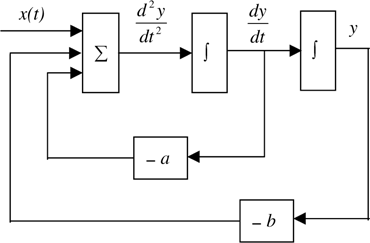
The first step in solving a differential equation using the analog computer technique is to develop the so-called analog computer simulation diagram. The process is straightforward. As a simple example, assume that a system is defined by the differential equation
where a and b are, for now, assumed constant. Solving the differential equation for d2y/dt2 gives
We then integrate d2y/dt2 to obtain dy/dt, and integrate dy/dt to obtain y(t). These quantities can then be multiplied, or otherwise manipulated, by appropriate constants or functions to form the terms necessary for representation of the various terms in (6.45). Combining them appropriately yields the differential equation and the analog computer simulation diagram. A little thought shows that the analog computer simulation diagram for our example differential equation is as shown in Figure 6.12. While Figure 6.12 was developed for (6.45), which is a simple linear equation with constant coefficients and is solvable using a variety of methods, the beauty of the analog computer technique comes from the fact that the technique is applicable to nonlinear and time-varying systems of arbitrary order.
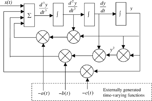
As an example of a system that is both nonlinear and time-varying, assume that a system of interest is defined by the differential equation
Solving for d3y/dt3 gives
from which the simulation diagram shown in Figure 6.13 immediately follows. The time-varying coefficients a(t), b(t), and c(t) can be specified by appropriate equations or may be files of measured data collected experimentally.
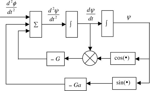
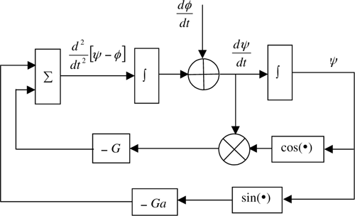
We now consider the simulation of the PLL using the differential equation approach. The first step is to derive the differential equation. From Figure 6.3 it follows that
Since the VCO in the PLL model illustrated in Figure 6.3 can be represented by an integrator, we have
Substitution of (6.48) in (6.49) and using (6.25) for the loop filter gives
We will simplify the problem slightly by assuming a “perfect” second-order loop for which λ = 0. This yields
Since multiplication by s is equivalent to differentiation in the time domain, we have the differential equation
By definition
and
Equation (6.52) can then be written
where ψ(t) is the PLL phase error and φ(t) is the phase deviation of the input signal. Prior to developing the analog computer simulation diagram, we first write the preceding equation in the form
The simulation diagram for this system is illustrated in Figure 6.14. We desire to examine this system with a step change in the input frequency deviation at t = t0. Thus, as before, we let
so that
Thus the input shown in Figure 6.14 is an impulse.
It is often desirable to place the input at a point in the simulation diagram that allows for a more straightforward simulation. For example, as previously shown, the input in Figure 6.14 is an impulse. Integrating the impulse and moving it to the right of the first integrator as shown in Figure 6.15 allows us to use the step function defined by (6.57) as an “equivalent input”. Simple modifications such as this can often significantly simplify a simulation.
Example 6.3.
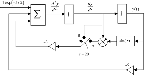
We end this chapter with a simulation of a system that is both nonlinear and time-varying. Assume that a system of interest is defined by the differential equations
and
The system is nonlinear because of the ![]() term in the equation defining the system for t < 20 and is time-varying, since the form of the differential equation is time-dependent. The fact that the system is characterized by two separate differential equations can be implemented by a switch that changes position at t = 20 seconds as shown in Figure 6.16. In position A the system is nonlinear, while in position B the system is linear. The phase plane will illustrate that, as expected, the response of a nonlinear system is quite different from the response of a linear system. As we know, solving nonlinear differential equations is a formidable task and we therefore resort to simulation. The MATLAB program to realize the example system is given in Appendix D. Note the similarity between this system and the second-order PLL. Since both systems are second order, two integrators are required in both cases. The only significant difference in the two systems is the equation at the output of the summing junction, which closes the simulation loop.
term in the equation defining the system for t < 20 and is time-varying, since the form of the differential equation is time-dependent. The fact that the system is characterized by two separate differential equations can be implemented by a switch that changes position at t = 20 seconds as shown in Figure 6.16. In position A the system is nonlinear, while in position B the system is linear. The phase plane will illustrate that, as expected, the response of a nonlinear system is quite different from the response of a linear system. As we know, solving nonlinear differential equations is a formidable task and we therefore resort to simulation. The MATLAB program to realize the example system is given in Appendix D. Note the similarity between this system and the second-order PLL. Since both systems are second order, two integrators are required in both cases. The only significant difference in the two systems is the equation at the output of the summing junction, which closes the simulation loop.
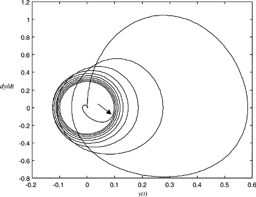
Executing the simulation program given in Appendix D results in the phase plane illustrated in Figure 6.17. Note that the phase trajectory both begins and ends at the origin (0,0). The point at which the switch changes, t = 20 seconds, is approximately indicated by the arrow. One sees that the phase plane approaches a limit cycle as indicated by the convergence of the phase trajectory to a closed loop. A system operating in the limit-cycle mode is an oscillator. The frequency of oscillation and the waveshape of y(t), or its derivative, can be determined by plotting the time-domain waveforms. Oscillation will continue as long as the switch is in position A.
Moving the switch to position B results in a linear system. At the time the switch is moved to position B (t = 20), the input is negligible [actually exp(−10)] and the system response closely approximates that of an unexcited second-order system, with the initial conditions given by the values of y(t) and ![]() at the time the switch is moved from position A to position B.
at the time the switch is moved from position A to position B.
Throughout this chapter we have used the trapezoidal numerical integration rule to approximate true integration. This was done for simplicity and, as mentioned earlier, the trapezoidal rule works quite well if the sampling frequency is sufficiently high. Other integration rules will be the subject of later study when a more general study of nonlinear systems is presented. (See Chapter 12.)
The trapezoidal integration rule, developed in the preceding chapter, gives us the capability to develop numerical solutions to differential equations. Since all lumped parameter systems can be described by a differential equation, it follows that a wide variety of systems can be simulated using trapezoidal integration to approximate continuous-time integration. Since the phase-locked loop is a fundamental building block of many communications systems, it provides a useful case study for illustrating a number of simulation concepts.
In order to develop a simulation model of the PLL, an analytical model must first be derived. The analysis required for model development also leads to an understanding of the basic operational characteristics of the PLL and, in turn, makes the simulation results understandable. Thus, the first two sections of this chapter focused on the development of an analytical model of the PLL. We saw that the major components of the PLL are the phase detector, the loop filter, and the voltage controlled oscillator. Two different phase detector models were developed, the sinusoidal phase detector and a generalized phase detector model based on the Fourier series expansion of the phase detector characteristic. It was shown that the VCO is an FM modulator. The loop filter and the loop gain control the PLL dynamics.
In general, the PLL is a nonlinear system with the nonlinearity resulting from the phase detector. Since the PLL is a nonlinear system, analysis using traditional analytical methods is difficult and we therefore turn to simulation. If, however, the phase error is small, system behavior becomes linear and the techniques of linear system theory are sufficient for analysis. Operation as a linear system is often referred to as tracking and nonlinear operation is referred to as acquisition. We therefore have two important PLL models, the nonlinear model, which is general, and the linear model, which can be used for those cases in which the phase error is small. The linear model is used to define the damping factor and the natural frequency of the second-order PLL.
Using a first-order PLL, for which the loop filter is zero order, the concept of a phase plane was introduced. The characteristics of the phase plane illustrated the mechanism by which the PLL achieves phase lock. It was shown that the first-order PLL has a finite lock range limited by the loop gain. As a result, the first-order PLL is not suitable for many applications. The second-order PLL has an infinite lock range and is widely used.
Prior to performing a simulation study of the second-order PLL, an architecture for the simulation code was developed. The simulation code is conveniently divided into three separate programs, a preprocessor, a simulation engine, and a postprocessor. The preprocessor is a short program through which the parameters necessary for defining the system under study and the parameters required to manage execution of the simulation are defined. The simulation engine contains the code for executing the simulation. The postprocessor takes the data produced by the simulation engine and generates the output required by the simulation user. Partitioning the code in this way makes the simulation software easier to maintain and understand. In addition, the three code segments can be developed in different languages, which makes it possible to match the choice of language to the task of the program.
An example simulation was performed for a second-order PLL. The cycle slipping phenomena was clearly observable from both the phase plane and the time-domain waveforms.
After considering the PLL, attention was turned to the more general problem of simulating systems from the differential equation. By solving for the highest derivative and using repeated integration, we saw that all terms in the differential equation can be generated and, therefore, the differential equation could be solved. This approach was widely used as a simulation technique for analog computers. The analog computer technique for simulating a system is very general and can be used for systems that are nonlinear and/or time-varying.
A large number books have been written that treat the phase-locked loop in detail. A small sampling of this list includes the following:
R. E. Best, Phase-Locked Loops: Theory, Design and Applications, New York: McGraw-Hill, 1984.
A. Blanchard, Phaselock Loops, New York: Wiley, 1976.
F. M. Gardner, Phaselock Techniques, 2nd ed., New York: Wiley, 1981.
D. R. Stephens, Phase-Locked Loops for Wireless Communications, Boston: Kluwer Academic Publishers, 1998.
A. J. Viterbi, Principles of Coherent Communications, New York: McGraw-Hill, 1966.
6.1 | Develop and run a simulation to verify the results presented in Figures 6.6 and 6.7. |
6.2 | Using simulation, determine the steady-state phase error for a first-order PLL with G = 40(see Figure 6.6). Estimate this value using the linear model. How do they compare? Repeat for G = 50 and G = 100. What do you conclude? |
6.3 | The results given in Figure 6.11 were obtained by executing the simulation program given in Appendix A together with the preprocessor and postprocessor given in Appendices B and C, respectively. A pole offset λ of 0.10 was assumed. An imperfect loop typically slips more cycles than a perfect loop and therefore takes longer to achieve phase lock. Examine the impact of the pole offset by executing the program assuming a perfect loop (λ = 0). Except for the pole offset use the same parameters as given in (6.40). How many cycles are slipped by the perfect loop? By how much is the lock time reduced? |
6.4 | Using simulation, determine the steady-state phase error for a second-order PLL with λ = 0.10 (see Figure 6.11 and consider using the |
6.5 | In this problem we wish to examine the effect of the sampling frequency on the simulation program given in Appendix A. As a first step execute the simulation using the parameters given in (6.40). Repeat the simulation using sampling frequencies of 50 Hz, 100 Hz, and 500 Hz. Comment on the results. Repeat the simulation using a sampling frequency of 10,000 Hz. What does this last simulation tell you? How can you determine that a suitable sampling frequency is being used? |
6.6 | In this problem we consider the use of the technique described in Example 6.1 to model the triangular phase detector characteristic illustrated in Figure 6.18. Determine the values of the |
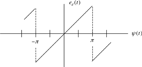
6.7 | Repeat the preceding problem for the sawtooth-wave phase detector input-output characteristic illustrated in Figure 6.19. As before, the slope of the input-output characteristic is +1 at all points except at odd multiples of π and it is periodic with period 2π. |
6.8 | Using the results of Problem 6.6, simulate a second-order PLL with a triangular-wave phase detector characteristic. Use the PLL parameters given in (6.40) that provided the results illustrated in Figure 6.11 for a sinusoidal phase detector. Compare the results obtained with the triangular-wave phase detector with those given in Figure 6.11. |
6.9 | Using the results of Problem 6.7, simulate a second-order PLL with a sawtooth-wave phase detector characteristic. As in the previous problem use the PLL parameters given in (6.40) that provided the results illustrated in Figure 6.11 for a sinusoidal phase detector. Compare the results obtained with a sawtooth-wave phase detector with those given in Figure 6.11. |
6.10 | Develop a signal-flow graph corresponding to Figure 6.15 and label the nodes that would be used in a simulation as was done in Figure 6.10. Using the signal-flow graph, write a MATLAB program for simulating the system and displaying the results. The preprocessor and postprocessor given in Appendices B and C, respectively, can be used. Execute the simulation for Δf = 40, fn = 10, |
6.11 | We previously saw that in order to break the computational deadlock resulting from the presence of feedback, a one sample delay had to be inserted in the feedback loop. This gave rise to the following expression defining the relationship between input phase, the VCO phase, and the phase detector output:
In many models of PLLs used at high frequencies it is appropriate to use the model
where kT represents “transport delay”. Transport delay results from the finite time required for a signal to propagate from one functional block to another functional block in a hardware implementation. In principle, transport delay accounts for the propagation delay around the loop that is not accounted for by the sum of the group delays of the functional blocks. Modify the simulation program given in Appendix A to include the effects of transport delay. Execute the simulation using the parameters defined by (6.40) and various values of transport delay. Since transport delay increases the time required to achieve phase lock, the value of |
6.12 | For the nonlinear time-varying system investigated in Example 6.3, determine the frequency of oscillation assuming that the switch has been in position “A” for a long time. Plot the waveforms for y(t) and dy/dt describing limit cycle behavior. |
6.13 | In Example 6.3 the limit cycle, because of the default axis scaling used by MATLAB very nearly approximates a circle in Figure 6.17. However, since the abscissa and the ordinate in Figure 6.17 are not scaled equally, the limit cycle is not a circle but an oval. Modify the program given in Appendix D so that the true shape of the limit cycle is revealed. What is the equation of the limit cycle? Can you justify this equation? |
6.14 | Two systems are to be compared assuming a common input. One system is defined by the differential equation and the second system is defined by By solving both differential equations subject to initial conditions, θ(0) = 1, dy(t)/dt|t=0 = 0, and d2y(t)/dt2|t=0 = 0, compare the responses of the two systems. |
6.15 | A Costas PLL, which is used for demodulation of DSB and PSK signals, is illustrated in Figure 6.20. The input signal is assumed to be
|
% File: c6_PLLsim.m
w2b = 0; w2c = 0; s5 = 0; phivco = 0;       % initialize
twopi  = 2*pi;                              % define 2*pi
twofs  = 2*fs;                              % define 2*fs
G = 2*pi*fn*(zeta+sqrt(zeta*zeta-lambda));  % set loop gain
a = 2*pi*fn/(zeta+sqrt(zeta*zeta-lambda));  % set filter parameter
a1 = a*(1-lambda); a2 = a*lambda;           % define constants
phierror = zeros(1,npts);                   % initialize vector
fvco = zeros(1,npts);                       % initialize vector

% beginning of simulation loop

for i = 1:npts
    s1 = phin(i) - phivco;           % phase error
    s2 = sin(s1);                    % sinusoidal phase detector
    s3 = G*s2;
    s4 = a1*s3;
    s4a = s4-a2*s5;                  % loop filter integrator input
    w1b = s4a+w2b;                   % filter integrator (step 1)
    w2b = s4a+w1b;                   % filter integrator (step 2)
    s5 = w1b/twofs;                  % generate filter output
    s6 = s3+s5;                      % VCO integrator input
    w1c = s6+w2c;                    % VCO integrator (step 1)
    w2c = s6+w1c;                    % VCO integrator (step 2)
    phivco = w1c/twofs;              % generate VCO output
    phierror(i) = s1;                % build phase error vector
    fvco(i) = s6/twopi;              % build VCO input vector

end

% end of simulation loop
freqerror = fin-fvco;                % build frequency error vector
% End of script file.% File: c6_PLLpre.m
clear all % be safe
disp(' ') % insert blank line
fdel = input('Enter the size of the frequency step in Hertz > '),
fn = input('Enter the loop natural frequency in Hertz > '),
lambda = input('Enter lambda, the relative pole offset > '),
disp(' ')
disp('Accept default values:')
disp(' zeta = 1/sqrt(2),')
disp(' fs = 200*fn, and')
disp(' tstop = 1')
dtype = input('Enter y for yes or n for no > ','s'),
if dtype == 'y'
zeta = 1/sqrt(2);
fs = 200*fn;
tstop = 1;
else
zeta = input('Enter zeta, the loop damping factor > '),
fs = input('Enter the sampling frequency in Hertz > '),
tstop = input('Enter tstop, the simulation runtime > '),
end
npts = fs*tstop+1; % number of simulation points
t = (0:(npts-1))/fs; % default time vector
nsettle = fix(npts/10); % set nsettle time as 0.1*npts
tsettle = nsettle/fs; % set tsettle
%
% The next two lines establish the loop input frequency and phase
% deviations.
%
fin = [zeros(1,nsettle),fdel*ones(1,npts-nsettle)];
phin = [zeros(1,nsettle),2*pi*fdel*t(1:(npts-nsettle))];
disp(' ') % insert blank line
%
% End of script file.% File: c6_PLLpost.m
kk = 0;
while kk == 0
k = menu('Phase Lock Loop Postprocessor',...
'Input Frequency and VCO Frequency','Input Phase and VCO Phase',...
'Frequency Error','Phase Error','Phase Plane Plot',...
'Phase Plane and Time Domain Plots','Exit Program'),
if k == 1
plot(t,fin,t,fvco)
title('Input Frequency and VCO Frequency')
xlabel('Time - Seconds'), ylabel('Frequency - Hertz'),
pause
elseif k ==2
pvco = phin-phierror;
plot(t,phin,t,pvco)
title('Input Phase and VCO Phase')
xlabel('Time - Seconds'), ylabel('Phase - Radians'),
pause
elseif k == 3
plot(t,freqerror);
title('Frequency Error')
xlabel('Time - Seconds'), ylabel('Frequency Error - Hertz'),
pause
elseif k == 4
plot(t,phierror);
title('Phase Error')
xlabel('Time - Seconds'), ylabel('Phase Error - Radians'),
pause
elseif k == 5
ppplot
elseif k == 6
subplot(211);
phierrn = phierror/pi;
plot(phierrn,freqerror);
grid;
title('Phase Plane Plot'),
xlabel('Phase Error /Pi'), ylabel('Frequency Error - Hertz'),
subplot(212)
plot(t,fin,t,fvco); grid
title('Input Frequency and VCO Frequency')
xlabel('Time - Seconds'), ylabel('Frequency - Hertz'),
subplot(111)
elseif k == 7
kk = 1;
end
end
% End of script file. % ppplot.m is the script file for plotting phase plane plots. If
% the phase plane is constrained to (-pi,pi) ppplot.m calls
% pplane.m.
%
kz = 0;
while kz == 0
k = menu('Phase Plane Options',...
'Extended Phase Plane',...
'Phase Plane mod(2pi)',...
'Exit Phase Plane Menu'),
if k == 1
phierrn = phierror/pi;
plot(phierrn,freqerror,'k')
title('Phase Plane Plot')
xlabel('Phase Error /Pi'), ylabel('Frequency Error - Hertz')
grid
pause
elseif k == 2
pplane(phierror,freqerror,nsettle+1)
pause
elseif k == 3
kz = 1;
end
end
% End of script file.function [] = pplane(x,y,nsettle)
% Plots the phase plane with phase in the range (-pi,pi)
ln = length(x);
maxfreq = max(y);
minfreq = min(y);
close % Old figure discarded
axis([-1 1 1.1*minfreq 1.1*maxfreq]); % Establish scale
hold on % Collect info for new fig
j = nsettle;
while j < ln
i = 1;
while x(j) < pi & j < ln
a(i) = x(j)/pi;
b(i) = y(j);
j = j+1;
i = i+1;
end
plot(a,b,'k')
a = [];
b = [];
x = x - 2*pi;
end
hold off
title('Phase-Plane Plot')
xlabel('Phase Error / Pi'), ylabel('Frequency Error in Hertz')
grid
% End of script file.Appendix D: MATLAB Code for Example 6.3
% File: c6_nltvde.m
w2b = 0; w2c = 0;                     % initialize integrators
yd = 0; y = 0;                        % initialize differential equation
tfinal = 50;                          % simulation time
fs = 100;                             % sampling frequency
delt = 1/fs;                          % sampling period
npts = 1+fs*tfinal;                   % number of samples simulated
ydv = zeros(1,npts);                  % vector of dy/dt samples
yv = zeros(1,npts);                   % vector of y(t) samples

% beginning of simulation loop

for i=1:npts
   t = (i-1)*delt;                           % time
   if t < 20
      ydd = 4*exp(-t/2)-3*yd*abs(y)-9*y;     % de for t<20
   else
      ydd = 4*exp(-t/2)-3*yd-9*y;            % de for t>=20
   end
   w1b = ydd+w2b;                            % first integrator - step 1
   w2b = ydd+w1b;                            % first integrator - step 2
   yd = w1b/(2*fs);                          % first integrator output
   w1c = yd+w2c;                             % second integrator - step 1
   w2c = yd+w1c;                             % second integrator - step 2
   y = w1c/(2*fs);                           % second integrator output
   ydv(1,i) = yd;                            % build dy/dt vector
   yv(1,i) = y;                              % build y(t) vector
 end}
% end of simulation loop

plot(yv,ydv)                          % plot phase plane
xlabel('y(t)')                        % label x axis
ylabel('dy/dt')                       % label y zaxis
% End of script file.
[1] Recall from basic communication theory that a bandpass limiter is often used at the input to a PLL in order to supress variations in the input envelope. This is, for example, the case when PLLs are used for FM demodulation.
[2] Recall that a proper function is one in which the degree of the denominator polynomial exceeds the degree of the numerator polynomial by at least one.
[3] A signal-flow graph is used rather than a block diagram simply for compactness.


