Chapter 3
Passive components
Chapter Outline
Limiting element voltage (LEV)
3.1.8 Fusible and safety resistors
Value tracking: thick film versus thin film
3.3.1 Metallized film and paper
3.3.7 Series capacitors and DC leakage
Consequences of self-resonance
3.4.2 Magnetic material definitions and metrics
Issues with unusual winding configurations
3.4.6 The danger of inductive transients
Protection against negative transients
3.1 Resistors
Resistors are ubiquitous. Because of this their performance is taken for granted; provided they are operated within their power, voltage and environmental ratings this is reasonable, since after millions of accumulated resistor-years’ experience there is little left for their manufacturers to discover. But there are still applications where specifying and applying resistors need to be handled with some care.
Let us start with an appreciation of the different varieties of resistor that are available. Table 3.1 is a guide to the common types that will be encountered in general circuit design. There are more esoteric types which are not covered.
Table 3.1 Survey of Resistor Types
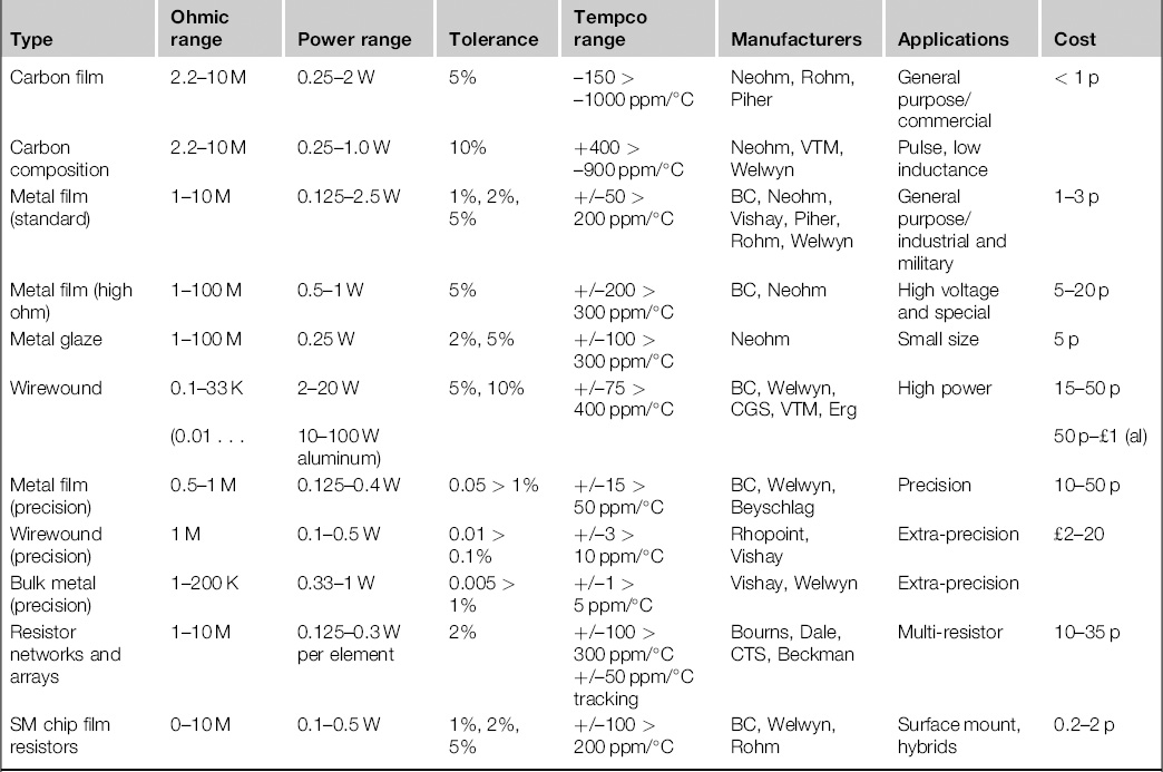
Notes:
1) This survey does not consider special resistor types.
2) Manufacturers quoted are those widely sourced in the UK at the time of writing.
3.1.1 Resistor types
Surface mount chip
The most common general purpose resistor is the thick film surface mount chip type. Available in huge quantities and very low prices, it is the workhorse of the resistor world. The construction is very simple (Figure 3.1) and hardly varies from manufacturer to manufacturer. An alumina (aluminum oxide ceramic) substrate with nickel-plated terminations has a resistive ink film printed or otherwise deposited on its top surface. The terminations are coated with a solder dip to ensure ease of wetting when the part is soldered into place, and the top of the part is coated with an epoxy or glass layer to protect the resistive element.
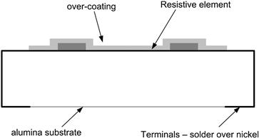
FIGURE 3.1 Chip resistor construction
Different manufacturers make various claims for the ruggedness and performance of their parts but the basic features are similar. Power dissipation is largely controlled by the thermal properties of the PCB pads to which the chip is soldered, and if you are running close to the rated power of the part it will be necessary to confirm that your pad design agrees with the manufacturer’s recommendations.
Common, standardized chip sizes are shown in Table 3.2. You can also get metal film chip resistors for higher performance applications, but these are more expensive than the common thick film.
Table 3.2 Chip Resistor Sizes
| Size | Dimensions (mm) (L × W × H) |
| 0201 | 0.6 × 0.3 × 0.25 |
| 0402 | 1.0 × 0.5 × 0.25 |
| 0603 | 1.6 × 0.8 × 0.45 |
| 0805 | 2.0 × 1.25 × 0.5 |
| 1206 | 3.2 × 1.6 × 0.6 |
| 1210 | 3.2 × 2.6 × 0.6 |
| 2010 | 5.1 × 2.5 × 0.6 |
| 2512 | 6.5 × 3.2 × 0.6 |
The resistive ink technique used for chips can also produce standard axial-lead resistors (metal glaze) of small size, and can be used directly onto a substrate to generate printed resistors. This technique is frequently used in hybrid circuits and is very cost-effective especially when large numbers of similar values are required. It is possible to print resistors directly onto fiberglass printed circuit board, though the result is of very poor quality and cannot be used where a stable, predictable value (compared with conventional types) is required.
Metal film
The next most common type is the metal film, in its various guises. This is the standard part for industrial and military purposes. The most popular varieties of leaded metal film are hardly any more expensive than carbon film and, given their superior characteristics, particularly temperature coefficient, noise and power handling ability, many equipment manufacturers do not find it worthwhile to bother with carbon film.
Variants of the standard metal film cater for high or low resistance needs. The “metal” in a metal film is a nickel–chromium alloy of varying composition for different resistance ranges. A film of this alloy is plated onto an alumina substrate. For leaded parts, the end caps and leads are force-fitted to the tubular assembly and the resistance element is trimmed to value by cutting a helical groove of controlled dimensions in it, which allows the same film composition to be used over quite a wide range of nominal values. The whole part is then coated in epoxy and marked. The disadvantage of the helical trimming process is that it inherently increases the resistor’s stray inductance, and also limits its pulse handling capability.
Chip metal film resistors use the same film-on-alumina technique but the trimming, if necessary, is done by cutting small, controlled segments out of the film element to increase its resistance slightly.
Carbon
The most common leaded resistor for commercial applications is the carbon film. It is certainly cheap − less than a penny in quantity. It also has the least impressive performance in terms of tolerance and temperature coefficient, but it is normally adequate for general purpose use. The other type which uses pure carbon as the resistive element is carbon composition, which was the earliest type of resistor but nowadays finds a use in certain applications which involve an assured pulse withstand capability.
Wirewound
For medium- and high-power (> 2 W) applications the wirewound resistor is almost universally used. It is fairly cheap and readily available. Its disadvantages are its bulk, though this allows a lower surface temperature for a given power dissipation; and that because of its construction it is noticeably inductive, which limits its use in high-frequency or pulse applications. Wirewound types are available either with a vitreous enamel or cement coating, or in an aluminum housing which can be mounted to a heatsink. Aluminum housings can offer power dissipations exceeding 100 W per unit.
Precision resistors
Once circuit requirements start to call for accuracy and drift specifications exceeding the usual metal film abilities, the cost increases substantially. It is still possible to get metal film resistors of “precision” performance up to an order of magnitude better than the standard, though at prices an order of magnitude or more higher. Drift requirements of less than 10 parts-per-million per °C (ppm/°C) introduce many more significant factors into the performance equation, such as thermal EMF, mechanical and thermal stress, and terminating resistance. These can be dealt with, and the resistive and substrate materials can be optimized, but the unit costs are now measured in pounds, and delivery times stretch to months.
Resistor networks
Thick-film resistor networks are manufactured like chips. A resistive ink is screen-printed onto a ceramic substrate to form many resistors at once, which is then encapsulated to form a multi-resistor single package. The resulting resistors have the same performance as a single thick-film chip, though with reduced breakdown voltage and power handling ability. However, it is also possible to manufacture metal film networks with very good accuracy and stability, and more importantly the property of closely tracking values over temperature.
3.1.2 Tolerancing
Perhaps the most fundamental application question is that of accuracy and tolerances. Process variations apply to all standard resistor manufacturers; for example, a single 68-K resistor will not have an absolute value of 68 000 ohms. If it is a 5% part its value when supplied should lie between 64.6 K and 71.4 K (and occasionally outside, if the manufacturer’s quality assurance isn’t up to scratch). What are the consequences of this, for example, for the humble potential divider shown in Figure 3.2, when the input voltage (Vi) is defined as 10 V?
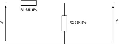
FIGURE 3.2 Simple potential divider
The unloaded value of VO is not 5 V. In the real circuit there are two worst-case values to take into account: when R1 is at the upper limit of its tolerance and R2 is at the lower limit, and vice versa. These two cases yield:
![]()
![]()
The general case is
![]()
where V is the output voltage with both resistors nominal, and V′ is the output voltage when R1 is at its high tolerance K and R2 is at its low tolerance K (for 5% resistors, K = 0.05). If the resistors are equal, the voltage variation is the same as the resistor tolerance.
You have to check that neither of these cases leads to out-of-limits circuit operation; and to be thorough, this must be done for all critical resistor combinations in the whole circuit. The trick, of course, is to know which combinations are critical. In a complex resistor network it is not always easy to see which permutations produce worst-case results. In such cases a circuit simulator can quickly prove its worth.
Basic statistical behavior
If we consider any parameter of a device or circuit as being defined by a single number, then this is defined as the nominal value. It is easy, particularly when an optimization has been used, to consider this an exact and precise definition of the model behavior. This is, however, an error in many cases, as in fact the nominal value is often simply the mean value obtained from multiple tests with a complete batch of components to establish the values.
For example, consider a batch of 1000 resistors which have been manufactured to have a designed value of 100 Ω. Each device is measured on a resistance bridge to establish its actual value, and if we plot the results we would in fact see a “spread” of results due to the intrinsic variability of the manufacturing process.
Clearly we can see that that the results of the measurement show a spread around the desired value of 100 Ω, but that in fact most of the results are not exactly the correct value and some results are quite some distance from the nominal value. If we take the same results and calculate a histogram of the values, then we can measure the mean value and also the standard deviation.
The calculation of the mean value for a continuous signal is the integration over a time period, however, in this case we are looking at a number of discrete values, so the integration becomes a summation as defined in Eq. (3.1):
 (3.1)
(3.1)
where n is the number of samples, x[i] is the individual sample and μ is the Mean value.
We also need to calculate the variability of the measurement, i.e. how much do the measurements deviate from the nominal value? To do this we need to calculate the variance from the nominal value using the expression defined in Eq. (3.2).
 (3.2)
(3.2)
The variance is not a particularly useful number as it is scaled (squared in fact) from the original units and so in order to get a measure of the variability, we take the square root of the variance to obtain a measure of the typical deviation of a sample from the mean value and this is called the standard deviation (σ) as defined in Eq. (3.3).
 (3.3)
(3.3)
If we take the results shown in Figure 3.3, and calculate the mean and standard deviation, we can superimpose them on the statistical “count” plot in Figure 3.4. We can see that the mean value is measured as 99.949 Ω and the standard deviation is measured as 3.3854 Ω.
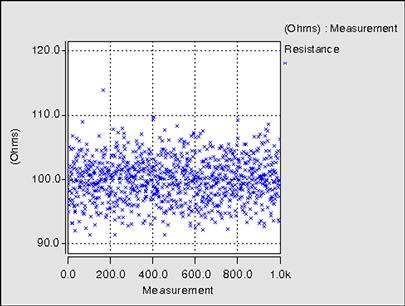
FIGURE 3.3 Random spread of resistance measurements
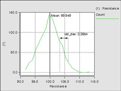
FIGURE 3.4 Mean value and standard deviation
A valid question that the circuit designer could ask at this point is what do these numbers actually represent? Clearly the mean value is useful as it demonstrates that on average the device is very close to our specified value of 100 Ω, however, in many cases the results deviate from this. The standard deviation is a useful measure in that it can be used to estimate the proportion of devices within a certain deviation from the nominal value. We can only make this assumption, however, if we have a well-defined statistical variation behavior. In practice we can say that a truly random variation will follow a statistical function called a “normal” distribution. This has, if there are enough samples, a bell curve shape with the probability density function (PDF) as defined by Eq. (3.4).
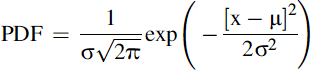 (3.4)
(3.4)
If we plot this graphically, we can see the symmetrical and smooth nature of the PDF of the normal distribution.
A key significant aspect of the PDF shown in Figure 3.5, is that we can quantify using this function proportionally how much of the values will be within one standard deviation of the mean, two standard deviations and so on. As we can see from Figure 3.6, 68.2% of the samples are within one standard deviation of the mean value, 95.45% are within two standard deviations and 99.73% are within three standard deviations. In fact, most engineering designers will work to a tolerance of three standard deviations, which leads to the term “six-sigma design”, which is to plus and minus three standard deviations (sigma).
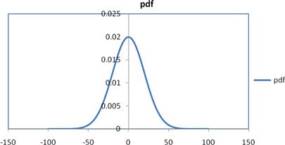
FIGURE 3.5 PDF of ideal normal distribution with mean value of 0 and standard deviation of 20
FIGURE 3.6 Proportions of samples with a normal PDF relative to the standard deviation
If we return briefly to our previous example of the resistor, where we have obtained a mean value of 99.949 Ω, and a standard deviation of 3.3854 Ω, we can therefore say that if we assume that the variation follows a normal distribution that over 99% of the values will fall in the range μ ± 3σ which is 99.949 Ω ± 10.1562 Ω. This indicates that we will see a spread of values mostly in the range 90–110 Ω, and if we return to Figure 3.3, we can see that this is indeed the case. In our 1000 samples, we can see that there is only one measurement that falls outside this range.
Modeling distributions
We can implement a probability distribution function on a parameter by applying a “normal” distribution directly to the parameter and passing this to the model. For example, if the resistance parameter is normally passed to the model using the mean value (in our example r = 100 Ω), we can instead pass the output from a normal distribution function (with the same mean value, but also with a “tolerance” value, which is the same as the 3σ value we calculated in the previous section). In this example we could therefore round the measured values to a mean value of 100 Ω and a tolerance (3σ) value of 10 Ω. This is implemented in the model as a normal function, as shown in Eq. (3.5).
![]() (3.5)
(3.5)
where in this case the normal function parameters are the mean value, mean – 3σ, and mean + 3σ.
Tolerance variations
It is sometimes tempting to hope that tolerance variations will cancel out over a medium-to-large sample, so that if a circuit parameter depends on several resistor values a sort of “average” tolerance which is less than the specified tolerance can be used. This is dangerously bad practice. Process similarities (the flip side of process variations) can often mean that a single batch of 5% resistors all have the same value to within, say, 1%, yet be 4% off their nominal value. This is quite a frequent occurrence, because the manufacturer may select parts for close tolerance purposes out of a batch of wider tolerance. What is left in the wide tolerance batch then has “holes” in the middle of the tolerance range. The manufacturer is perfectly entitled to ship them, but your test department will find a whole batch of assemblies built with perfectly good components and all showing the same fault.
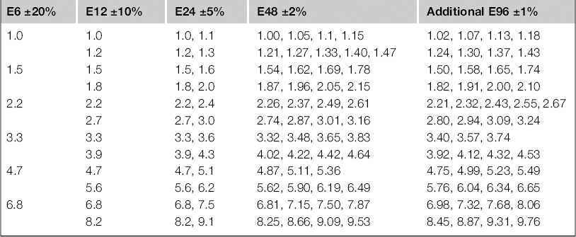
If the standard 5% thick-film tolerance is not good enough, there is the option of the (slightly) more expensive 2% or 1% metal film types. Indeed, the price differential between these is now so small as a proportion of the overall cost of an assembly that it is common to standardize on the 2% or 1% ranges for all applications, regardless of the actual requirement. One point to note is that extreme low or high values may not be available in the tighter tolerances. Below 1% tolerance the field is taken over by precision resistors which are often specified to have a particular required value, rather than being only available in the standard values. The standard value range specified by IEC 60063 is given in Table 3.3.
Table 3.3 IEC 60063 Standard Component Values
3.1.3 Temperature coefficient
Where precision resistors are needed, usually in measurement applications, another parameter becomes important: their resistive temperature coefficient (tempco), expressed in parts per million per °C (ppm/°C).
Standard metal film and chip resistors have tempcos of the order of ± 50 to ± 200 ppm/°C. The value of a 200 ppm/°C part could change by up to 1% over a temperature range of 50°C. This does not mean that every resistor quoted at 200 ppm/°C will change by this much, only that this is the maximum that you can expect. The actual temperature coefficient depends on the manufacturing process and also on the value. For instance, carbon film tempco varies from −150 to −1000 ppm/°C depending on value. Precision wirewound, metal film and bulk metal resistors can achieve orders of magnitude better than this − 1 ppm/°C is achievable − but are correspondingly expensive.
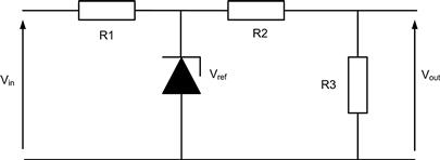
FIGURE 3.7 Stable voltage reference divider circuit
A typical use for precision resistors is in dividing down a stable voltage reference (Figure 3.7 for example). There is no point selecting a voltage reference with a tempco of 30 ppm/°C and then dividing it down with 200 ppm/°C resistors. The type used for R1 in this circuit is not critical as input voltage regulation will usually be far more significant than value changes. On the other hand, if Vout is to be used as a reference derived from Vref, then R2 and R3 must be of comparable stability to the reference voltage. Suppose that Vout is required to be 1.00 V ± 1.5% and to show 30 ppm/°C temperature stability. The reference is an LM385B–1.2 which has a specified voltage of 1.235 V ± 1% and an average temperature coefficient of 20 ppm/°C.
To get 1.00 V with nominal values and assuming R3 = 10 K with no load current, then R2 will need to be 2.35 K (not a standard value, though the closest in the E96 series is 2.37 K). Taking worst-case tolerances for the LM385 and both resistors (Vref high, R2 low, R3 high; Vref low, R2 high, R3 low) and assuming both resistors have the same tolerance, then some calculation shows that the specified resistor tolerance should be better than 1.4%. Similarly the tempcos should be better than 26 ppm/°C. These requirements would point to the use of 1% 25 ppm metal film types.
Temperature changes can come either from ambient variations (including other nearby components) or from self-heating due to dissipated power. Any application which requires good resistance value stability should aim for minimum, or at least constant, power dissipation in the component. Manufacturers’ data normally show a graph of temperature rise versus power dissipation for a given resistor type and this should be checked if value stability has to be maintained through changes in dissipation.
3.1.4 Power
Power dissipation is, of course, one of the most important specifications a designer has to check for each component. Power dissipation results in temperature rise, which is determined by how fast the heat is conducted away from the body. The maximum body temperature usually occurs in the middle of the resistor, and this is known as the hot-spot temperature. Prolonged high temperatures (remembering that the quoted hot-spot temperature must be added to the maximum ambient) cause two things: a reduction in reliability, not only of the resistor but of components near it, and a resistance shift.
A good rule-of-thumb for a reliable circuit is never to allow a dissipation of more than half the rated power in each component; many companies have their own in-house rules based on experience or customer’s specifications.
Power should be calculated under worst-case operating conditions: for example a resistor may be placed across a nominally 12-V supply rail which under extreme conditions could reach 17 V. The difference in power dissipation is nearly double.
3.1.5 Inductance
In some applications, other performance factors must be taken into account. The construction of carbon and metal film leaded resistors is basically a helix cut into a resistive film on a tubular ceramic substrate (Figure 3.8). The dimensions of the helix, together with the bulk resistance of the film, determine the actual resistance element value. Such a form effectively provides a low-Q inductor. When the frequency of circuit operation extends into the RF region, the reactance can become a significant part of the total impedance, and non-inductive resistors must be used.
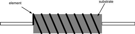
FIGURE 3.8 Helical construction of film resistors
The easiest way to obtain this is to choose a carbon composition type, where the resistive element is a homogeneous block of carbon, so that component inductance is primarily that due to the leads. Early carbon compositions have now mostly been superseded by ceramic–carbon types which, rather than a hot-molded solid carbon block, use a carbon conductor mixed with a ceramic filler; different values are obtained by altering the ratio of filler to conductor. For more demanding requirements you need to use special non-inductive metal film or foil resistors. Chip resistors exhibit inherently low inductance because of their small size and are usually adequate for RF applications if their handling requirements and power ratings are suitable.
3.1.6 Pulse handling
Another application where conventional helical-cut film resistors, and indeed ordinary small chip resistors, are unsuitable is in pulse applications, where a high voltage must be withstood for short durations, so that the average power dissipation is small though the peak power is many times larger. A common application of this sort is in thyristor, triac or power transistor snubbers for high-voltage switching. The standard snubber circuit is shown in Figure 3.9.
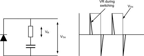
FIGURE 3.9 The snubber circuit
The RC combination restricts the rate-of-rise of voltage across the device during inductive switch-off, but in so doing the resistor is faced with a momentary fast voltage spike, which approaches the power supply voltage. This can cause arcing between adjacent turns of the helix of a film resistor, and swift breakdown of the whole unit. Use of a wirewound high-power component in this application is ill-advised because the high self-inductance of the resistor creates a tuned circuit which, although it has a low Q, can actually increase the transient voltage seen by the device. Again, a carbon composition type suffers less from both the breakdown mode and the inductance. Other chip and metal glaze resistors are available with specifically characterized pulse response. Applications such as telecoms protection, where a series resistor is used to protect an input circuit from applied high-voltage surges which may occur only very occasionally, also call for such pulse characterization.
Limiting element voltage (LEV)
The LEV is the maximum continuous voltage that can be applied to a resistor. For lower values the power rating is exceeded before the LEV is reached, but with higher values the LEV imposes limits on the applied power. For instance, a 470-k 0.33-watt 1206-size resistor requires 394 volts to dissipate its rated power; but such a part commercially available has an LEV of 200 V, so this can in fact only dissipate (continuously) 85 mW. The LEV limit becomes more significant with pulsed applications of lower-valued resistors where the average power dissipated may be very low, but the peak applied voltage can exceed the LEV.
Pulse applications may stress the power rating of the resistor as well as the voltage; the average power dissipated is equal to the peak power times the duty cycle of the pulses, but for pulse duration longer than a millisecond or duty cycles in excess of 10 or 20, the average power permissible has to be derated from the theoretical. Different types of resistor construction suffer in different ways. For instance wirewound or film types must dissipate all the applied power in the conductor itself, rather than letting the heat out through the body of the resistor, since it takes a finite time for the heat to pass from the conductor into the body. As the mass of the wire or film is low, the energy-handling capability is also low and the derating is significant. Some manufacturers publish curves to allow this derating to be calculated.
For repetitive pulses you need to relate the average power in the pulse to the rated power of the resistor. This can be done for rectangular or exponentially decaying impulses as follows:
![]()
![]()
where V is the peak pulse voltage, R is the nominal resistance, T is the pulse period (so 1/T is the pulse repetition rate), τ is the impulse duration of a rectangular pulse and τ0 is the time constant to 0.37×V of an exponential pulse.
3.1.7 Extreme values
Very low values
A typical application for low-value resistors is in current sensing. You often need to control or monitor a power supply current of a few amps with the minimum possible voltage drop, for power efficiency reasons; a low value resistor of, say 10 mΩ will develop 50 mV when 5 A is passed through it and this can be amplified by a precision differential amplifier and used for monitoring. Bulk metal resistors are available in flat chip form or as solder-in wire with values down to 3 mΩ and power ratings of 1–10 W.
There are some precautions to take with such low values. To achieve an acceptable accuracy it is normally necessary to make a four-terminal or “Kelvin” connection, so that the current carrying tracks and the voltage sense tracks go separately to the pads (Figure 3.10). An easy way to do this for through-hole components is to use opposite sides or different layers of the PCB for the two purposes, or at least to connect to opposite sides of the pad. Even when this is done, there is still some pad area and solder in series with the actual resistor element, which could compromise accuracy and/or tempco. To get around this, specify a component actually designed to have four terminals.
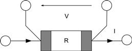
FIGURE 3.10 The Kelvin connection
The low-impedance, low-level-voltage sense is susceptible to magnetic field interference, and to control this you should minimize the loop area between the sense resistor and the sense circuit input. When you are monitoring AC signals with a few mΩ of resistance, the self-inductance of the resistor itself may become significant. For instance at, say, 400 Hz (a common aerospace AC power frequency) the impedance of a stray inductance of 100 nH is 0.25 mΩ, which could give a 5% error on a voltage measured across a 5 mΩ sense resistor. This makes wirewound types unattractive and bulk metal or chip resistors are to be preferred.
Finally, a metallic element with a high dissipation and a low sense voltage may give rise to thermoelectric errors. The junction between the element and its termination is a thermocouple, generating a voltage across it proportional to temperature. So a sense resistor in fact includes two thermocouples back-to-back, one at each terminal. As long as the temperatures at each termination are the same, their errors cancel out. This means that you should aim for thermal symmetry in the layout, by offering similar heatsinking to each terminal (via the PCB tracks, usually) and by keeping other heat sources distant.
Very high values
Different considerations apply to multi-megohm resistors. Here, the main problem is leakage due to contamination across the terminals. The highest values (up to 1014 ohms) are encapsulated in glass envelopes and it is necessary to avoid handling the glass, and to touch only the leads, to prevent finger grease from affecting the resistance across the terminals. Electrically, it is helpful to have a “guard” electrode around the resistor to act as an electrostatic shield and to reduce or null out the effects of leakage current into the terminals. High-value resistors have long time constants, and even a small amount of self-capacitance can have a significant effect: for instance a 100-GΩ resistor with a self capacitance of only 1 pF has a time constant of 0.1 seconds.
3.1.8 Fusible and safety resistors
There are some applications where a resistor is used in series with a power circuit to provide both a circuit function and a safety function. For instance, it may provide an inrush current limiter in a power supply input, so that a short-duration surge current at switch on is limited in value; and it may also provide a sacrificial component that fuses in the presence of a prolonged fault current, for instance if the input diode bridge or electrolytic capacitor fails. Under these circumstances a resistor should be specified principally for a predictable fusing characteristic, i.e. the time it takes to go open circuit for a given energy duration (see also Section 7.2.3). It is often necessary to be sure that the component will be flameproof when it fuses so that there is no fire hazard. Metal oxide and metal film components are available with these parameters fully characterized.
3.1.9 Resistor networks
A section on resistors would be incomplete without mention of the resistor network. There are two main advantages to resistor networks: production efficiency, and value matching/temperature tracking.
Production efficiency
Design for production is a subject in itself, more fully covered in Chapter 9. For leaded components, handling and insertion costs can be a significant fraction of the total cost of a PCB assembly. A single resistor whose purchase cost is less than 1 p may cost as much as 5−10 p once it has been inserted, depending on how production costs are calculated. If several resistors can be combined in one package then the overall cost of the package plus one insertion can easily be less than the cost of several resistors plus several insertions. To properly evaluate this trade-off you need to have an accurate knowledge of your particular production costs. Chip components in surface mount assemblies have a quite different arithmetic, since handling and placement on the board are usually automatic and the cost per part may well be negligible.
Usually resistor networks combine several resistors of one value in a package, dual-in-line or single-in-line, either all separate or with one terminal commoned. An obvious application for the latter type is for digital bus or I/O pull-ups. Linear circuits can benefit as well, especially if they can be designed to use several resistors of one value rather than a mixture of similar values.
One point to be wary of is the occasional temptation to use resistor networks too widely, so that they “gather up” what would otherwise be widely separated individual components. This is attractive for production, but often disastrous for the board layout, since undesirably long tracks might be needed to get the signal to and from the network. There will often be a trade-off to make between this aspect and the demand to minimize insertion costs.
Value tracking: thick film versus thin film
Resistor networks are available using two technologies: the universal thick-film type and the less widely available thin film. Thick-film networks have no better tolerance and drift specifications than conventional resistors, and so cannot be used in demanding applications. However, because all resistors in a package are constructed by simultaneously screen-printing a resistive ink onto a substrate, manufacturers can guarantee a better tempco tracking between resistors than an absolute tempco for each resistor. A typical performance is 250 ppm/°C individually, but a tracking of 50 ppm/°C, i.e. all resistors within the package will exhibit the same tempco to within 50 ppm/°C. Thin film types can show an order of magnitude better performance.
This feature can be made use of in precision amplifier circuits, and in some instrumentation amplifiers it is essential in order to meet performance requirements. Consider the differential op-amp configuration of Figure 3.11.
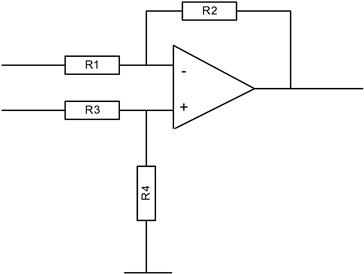
FIGURE 3.11 Basic differential op-amp configuration
For optimum common-mode rejection the ratios R1/R2 and R3/R4 must be equal; for unity gain all resistor values should be equal. Equality must be maintained over the operating temperature range. While it would be possible to use separate precision resistors of sufficient stability, the absolute value of the resistors is not critical, only their ratios. Since resistor networks can have a much better tempco tracking performance than absolute value, they are highly suited to this type of application. Indeed, some manufacturers offer special networks with different values in the package with guaranteed ratios, especially for such circuits.
Multiples of the package value can be easily obtained by parallel or series connection, and the overall tracking of resistor values is not impaired. If, for example, both half and quarter of the same reference voltage are required, the best circuit for stability and accuracy would have a potential divider in which all resistors were part of the same package (Figure 3.12).
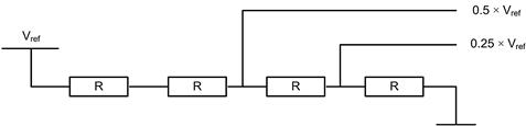
FIGURE 3.12 Potential divider using equal value resistors
3.2 Potentiometers
Potentiometers are one of the last bastions of electro-mechanical components in the face of the avalanche of digital silicon. They are bulky, unpredictable and unreliable, and can be a problem in fast circuitry; parasitic effects abound, and you can really only use them where the signal frequency times the circuit resistance is less than 106 Hz-Ω. They add time and money at the test and calibration stage of the production cycle. Many of their functions can be taken over by microprocessor-controlled digital equivalents. For instance, a classical use for the standard trimpot is to null out that bugbear of analog amplifiers, the offset voltage. In the days when op-amps had offsets measured in tens of millivolts, this was a very necessary function. But op-amps are now available at reasonable prices with offsets below half a millivolt, and if this is not enough it is often feasible to use a chopper stabilized device whose effective offset is limited only by thermal effects to a few microvolts. Alternatively, the intelligence of a microprocessor can be used to dynamically calibrate out the offset of a cheap op-amp by frequently auto zeroing the entire A–D subsystem. Equally, the gain of a network can be trimmed using a resistive D–A converter rather than a trimpot.
Nevertheless, there will remain applications where a pot is overall the best solution to a given circuit problem: digital implementations have been eschewed for other reasons, or the inherent linearity and lack of distortion of a passive resistor element are essential, or assured non-volatility of a setting is required. For these purposes, you need to consider the different types available.
3.2.1 Trimmer types
Potentiometers can be divided into two classes. Those types which are mounted on the circuit board and are only intended for adjustment on test and calibration, or possibly by maintenance technicians, are known as trimmers and are distinguished by their small size: quarter-inch-diameter units are commonplace and 3 mm2 surface-mount types are now on the market.
Carbon
The cheapest and lowest-performance types have a molded carbon film track and are of open construction (sometimes known as “skeleton” construction). They are prone to mechanical and environmental degradation and are therefore not suitable for professional applications, but their low cost (approaching 5 p in quantity) makes them popular in non-critical areas.
Slightly more expensive (about 20% more) are the enclosed carbon versions which protect the track from direct contamination but are otherwise similar to the skeleton type. Value tolerance for all carbon film trimmers is normally ±20%.
Cermet
The most popular type for commercial and professional purposes is the cermet. Several mounting versions and sizes, all multiple-sourced, are available, with costs ranging from 20 p to 80 p for single-turn variants. The term “cermet” refers to the resistive element, which is a METal film deposited on a CERamic substrate.
The cermet offers a wide range of resistance, from 10 Ω to 2 MΩ, with tolerances usually of ±10%, though cheaper parts offer ±20% and tighter tolerances can be ordered. Because it can be obtained in small sizes with low self-capacitance, it is useful at higher frequencies than other types.
Wirewound
The main advantages of wirewound trimmers are their low temperature coefficient, higher power dissipation, lower noise, and tighter resistance tolerance. When used as a variable resistor, their lower contact resistance improves the current-carrying capability through the wiper (cf. Section 3.2.3). Their resistance stability with time and temperature is slightly better than cermet, but the high-resistance extreme is comparatively low (50 kΩ) and the type is not suitable for high frequency. Their resolution is poor and they are also somewhat more expensive and less widely sourced than cermet.
Multi-turn
Both cermet and wirewound trimmers are available in multi-turn configuration. This means that more than 360° mechanical adjustment is needed to cause the wiper to traverse the total resistance element. (Note that a single-turn trimmer normally offers less than 270° adjustment angle.) You will commonly find 4, 10, 12, 15, 20 and 25 turn units. These are used when better adjustability is required than can be offered by a single-turn, but at somewhat greater cost and size, typically twice as much.
3.2.2 Panel types
The other potentiometer classification applies to those which are to be adjusted by the user, and therefore have a spindle which protrudes through the equipment panel. These can be mounted on the panel using an integral bush, or directly to the PCB. The latter tends to put extra strain on the pot’s terminals, and requires careful consideration of mechanical tolerances, but is popular because it dispenses with a wiring loom and therefore speeds up production time. The spindle can be insulated or of metal, with or without a locating flat for the knob; insulated types offer a potential safety and EMC advantage, but are also less mechanically rigid.
Carbon, cermet and wirewound
The electrical characteristics of these types are similar to those of single-turn trimmers of the same construction. Because the size of panel pots is necessarily larger to allow for mechanical strength and easy mounting, they can have higher power ratings than trimmers; 0.4 W is typical for carbon types, while cermets and wirewounds offer 1−5 W.
Conductive plastic
When you need a very-high-quality track construction, then the conductive plastic type is suitable. These offer very long life and low torque and are also suitable for position transducers. High-accuracy components are very expensive, but general purpose ones can be competitive with good-quality cermet types.
3.2.3 Pot applications
Firstly, remember that the wiper contact is the weakest point. Enormous advances have been made in potentiometer reliability over the years, and the cermet construction has proved itself in many applications. But the wiper is still essentially an electro-mechanical component and as such is the source of virtually all pot problems.
The golden rule is: draw as little DC through the wiper as you possibly can. If you have to draw significant current use a wirewound device. If the pot is used as a variable potential divider to set a circuit voltage, ensure that it is operating into a high impedance. If it is used in a signal path to vary signal amplitude, incorporate a DC blocking capacitor to prevent any DC flow through the wiper. The wiper/element contact has an unpredictable resistance of its own (Figure 3.13), which is affected by oxidation and electrochemical corrosion, and the effect of this resistance on the circuit (usually manifested as noise) must be minimized.
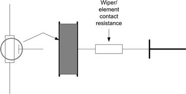
FIGURE 3.13 Potentiometer contact resistance
The less current that is drawn through the wiper, the less it will contribute to any noise voltage. Unfortunately, for some types a minimum current (such as 25 μA) should be drawn through the wiper, in order to “wet” the contact. This should be kept low.
Use as a rheostat
Secondly, if the pot is being used as a variable series resistor (historically called a “rheostat”), connect the wiper to one end of the track. This is a very simple precaution – one short length of pc track. The reason is that under conditions of age, dirt or extreme vibration the wiper can become temporarily (or even permanently) disconnected from the element track. If it is connected as in Figure 3.14(a), the maximum circuit resistance is limited to the end-to-end resistance of the pot. If you connect it as in (b), then the device can become open-circuit. In some circuit configurations this is merely a nuisance, but in others it could be catastrophic.
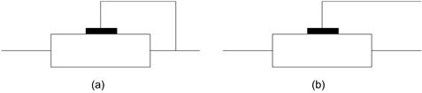
FIGURE 3.14 Rheostat connection
In this mode, the current passes almost entirely through the wiper and this can be a limiting factor in the circuit. Make sure the wiper current is limited to that given in the pot’s specification. If this isn’t available, you can safely assume that it is the current that would produce maximum power dissipation, if applied through the wiper only, with as a rule of thumb an absolute maximum of 100 mA for small trimmers. Also, remember that pots exhibit an “end resistance” which prevents wiper access to the ends of the resistance element. This restricts the minimum and maximum range that can be obtained: it is impossible to get a potentiometric division ratio (at “minimum volume”) of zero.
Adjustability
Do not expect infinite adjustability from your pot. A cermet element is theoretically capable of infinite adjustment, but test and calibration technicians will find a center-zero reading elusive, and the test and calibration labor costs will multiply, if you try to obtain more resolution from the pot than is realistically achievable. A multi-turn trimmer offers a better solution in this respect (Figure 3.15). Resolution is also compromised by shock- and vibration-induced jumps. If you use a wirewound element, don’t even think about high resolution, think of it more like a 100-way resistance switch.
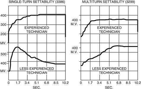
FIGURE 3.15 Settability of single- and multi-turn trimmers
(Source: Bourns, Inc.)
As is emphasized in the section on design for production, one of the major aims for any designer must be to make their design cheap to produce. Any trimming adjustment is a production cost and the time taken to do it must be minimized. The fewer trim adjustments there are, the better the design. But, when you are selecting a trimmer and determining its placement on the board, keep in mind the people who will have to use it and ensure that the adjustment screw is accessible. Place side-adjustment pots on the edge of the board and top-adjustment ones in the middle.
For best performance, use a series fixed resistance with a trimmer to provide only the range of adjustment required by the application – don’t use the trimmer to give you all the necessary resistance just to avoid one extra fixed resistor.
Law accuracy
The two common potentiometer laws are linear and logarithmic. These refer to the law which relates angular displacement to proportion of total track resistance at the slider. For linear pots, the law accuracy is specified as linearity and is closely related to cost; a low-cost panel component will probably not specify linearity at all and it is likely to be no better than 10%. Logarithmic pots are generally only intended for use as audio volume controls and the adherence to a log law will be even less accurate. If you need high law accuracy, for instance because you are using the pot as a position transducer, you will need to specify and pay for it. Linearities better than 1% are possible, but a typical high-quality component will offer no better than 5%. Note that the specification tolerance is a different parameter, as it refers only to the tolerance on the end-to-end resistance of the track.
Manufacturing processes
Another factor which works against potentiometers is their dislike of board soldering and cleaning processes. This of course applies to any electro-mechanical component: relays and switches are equally susceptible. When a board is being soldered, it and the components it carries are exposed to extreme temperature shocks; once it has been soldered it carries flux residues which must be removed by washing in water or solvent. Electro-mechanical components can be sealed or open. If they are sealed, there is the danger of a damaged seal allowing ingress of washing fluid which then remains and causes an early failure of the component. If open, the danger is that the washing fluid will directly affect the component’s operation. Either case is unsatisfactory and many manufacturers prefer to add electromechanical components by hand, for reliability reasons, after the rest of the board has been populated, soldered and cleaned − which is clearly an added production cost.
3.3 Capacitors
Like resistors, capacitors can tend to be taken for granted. There is as much a profusion of capacitor types and sub-variants as there is of resistors, and it is often hard to select the optimum part for the application. Table 3.4 shows the characteristics and applications of the more common types.
Table 3.4 Survey of Capacitor Types
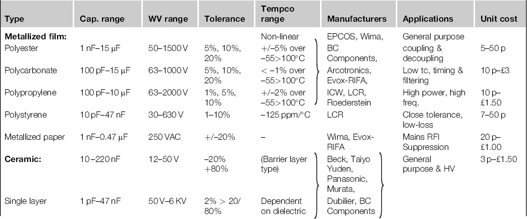
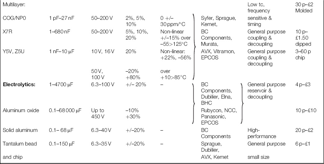
Notes:
1) This survey does not consider special types.
2) Manufacturers quoted are those widely sourced in the UK at the time of writing.
Capacitors can be subdivided into a number of major types and subheadings within those types. The divisions are best made by dielectric:
Film: Polyester, Polycarbonate, Polypropylene, Polystyrene
Ceramic: Single layer: barrier layer, high-K, low-K
This list covers all of the common types likely to be used in general-purpose circuit design. There are certain special or obsolete types − porcelain, trimmer, air dielectric, silver mica − which are not included because their applications are too specialized. The divisions listed above are further subdivided depending on their construction − chip, radial lead, axial lead, disc, or whatever − but this does not affect their fundamental circuit characteristics, although it becomes important when PCB layout and production processes are considered.
3.3.1 Metallized film and paper
For a survey of the applications, let us start with the film types. These all have the same general construction, a sandwich of dielectric and conductive films wound into a roll and encapsulated along with their connecting wires, as shown in Figure 3.16. There are two common methods of providing the electrode: one has a separate metal foil wound with the film dielectric, the other has a conductive film metallized onto the dielectric directly. The film and foil construction requires a thicker dielectric film to reduce the risk of pinholes, and therefore is more suitable to lower capacitance values and larger case sizes. Metallized foil has self-healing properties − arcing through a pinhole will vaporize the metallization away from the pinhole area − and can therefore utilize thinner dielectric films, which leads to higher capacitance values and smaller size. The thinnest dielectric in current use is of the order of 1.5 μm.
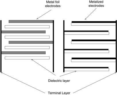
FIGURE 3.16 Film capacitor construction
Polyester
Of the film dielectrics listed the most common is polyester. This has the highest dielectric constant and so is capable of the highest capacitance per unit volume. It approaches multilayer ceramic capacitors for volumetric efficiency and in fact can be used in most of the same applications: decoupling, coupling and by-pass, where the stability and loss factor of the capacitor are not too important.
Polyester has a non-linear and comparatively high temperature coefficient. Its dissipation factor tan δ (see Figure 3.17) is also high, of the order of 8 × 10³ at 1 kHz and 20°C, and varies markedly with temperature and operating frequency. These factors make it less useful for critical circuits where a stable, low-loss component is needed.
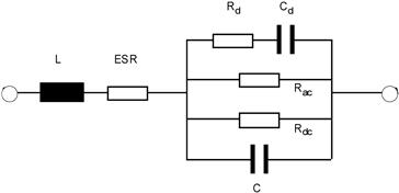
FIGURE 3.17 The capacitor equivalent circuit
C is the “ideal” capacitance of the device
Rac is the equivalent resistance due to AC dielectric losses, and may vary non-linearly with frequency and temperature; it is usually combined with ESR for electrolytic capacitors
Rdc is the leakage or isolation resistance of the dielectric, and may vary with temperature
ESR is the equivalent series resistance due to the electrode, lead and terminating resistances
L is the equivalent series inductance (ESL) due to the electrodes and leads
Rd, Cd are equivalent components to represent dielectric absorption properties
Capacitor specifications:
Temperature coefficient is the change in capacitance C with temperature and may be quoted in parts per million (ppm)/°C or as a percentage change of C over the operating temperature range
tan δ is a measure of the lossiness of the component and is the ratio of the resistive and reactive parts of the impedance, R/X, where X = ωC
Insulation resistance or time constant is a measure of the DC leakage and may be quoted as the product Rdc × C in seconds or as Rdc in MΩ. Leakage current describes the same characteristic, more usually quoted for electrolytics
Dielectric absorption is a measure of the “voltage memory” characteristic, which occurs because dielectric material does not polarize instantly, but needs time to recover the full charge; it is defined as a percentage change in stored voltage a given time after the sample is taken.
Polycarbonate
For these cases polycarbonate is best suited. This has a near flat temperature − capacitance characteristic at room temperature, with a decrease of about 1% at the operating extremes. It also has a lower tan δ, typically less than 2 × 10⁻³ at 20°C, 1 kHz. Polycarbonate would normally be specified for frequency-sensitive circuits such as filters and timing functions. It is also a good general-purpose dielectric for higher-power use, but in these applications polypropylene comes into its own.
Polypropylene and polystyrene
Polypropylene has a lower dielectric constant than the others and does not metallize so easily, and so gives a larger component for a given CV product. Also it exhibits a fairly constant negative temperature coefficient of −200 ppm/°C which restricts its use in frequency-critical circuits, although a defined tempco can be useful for temperature compensation in some instances. Its main advantage is its very low dissipation factor of around 3 × 10⁻⁴ at 20°C and 1 kHz, almost constant with temperature. This allows it to handle much higher powers at higher frequencies than the other types, so it is suitable for switch-mode power supplies, TV line deflection circuits and other high-power pulse applications.
Polypropylene capacitors can also be made to close tolerances and this makes them competitors to polystyrene in many tuned circuit and timing applications. Additionally, both polypropylene and polystyrene have similar temperature coefficients and loss factors (polystyrene tempco −125 ppm/°C, tan δ typically 5 × 10⁻⁴). They also both show a better dielectric absorption performance (0.02% to 0.03% − see Figure 3.17) than the other film types, which makes them best suited to sample-and-hold circuits. Both types suffer from a reduced high temperature rating, generally limited to 85°C, though some polystyrene types are restricted to 70°C and some polypropylene types are extended to 100°C. Suppliers of polystyrene types are scarce and it is rarely used.
Metallized paper
A further capacitor type which is often bracketed with film dielectrics is the metallized paper component. Paper was historically a very widely used dielectric, particularly in power applications, before the technical developments in plastic films superseded it. The great advantage of plastic films is that they absorb moisture very much less readily than paper, which has to be impregnated to prevent moisture ingress from destroying its dielectric properties. Paper is now mostly reserved for use in special applications, particularly for across-the-line mains interference suppressors. When a capacitor is used directly with a continuous connection across the mains, a fault in the dielectric or a transient overvoltage stress can lead to localized self-heating and eventually the component will catch fire, without ever blowing the protective mains fuse. This has been found to be the cause of many electrical equipment fires and much investigation has been carried out (prompted by insurance claims) into the question of capacitor flammability. Paper has excellent regenerative characteristics under fault conditions; very much less carbon is deposited by a transient dielectric breakdown than is the case for any of the plastic film dielectrics, so that self-heating is minimal and the component does not ignite. Metallized paper is therefore the preferred construction for this application, although polyester, polypropylene and ceramic suppressor types are available.
3.3.2 Multilayer ceramics
Multilayer ceramics have a superficially similar construction to film capacitors, but instead of being wound, layers of dielectric and electrode material are built up individually and then fired to produce a solid block with terminations at each end (Figure 3.18). For this reason they are often called “monolithic” capacitors. They can be supplied either in chip form or encapsulated with leads; the encapsulant can be a molded body or a dip coating.
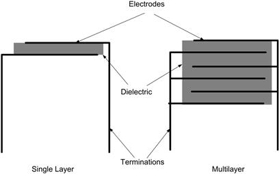
FIGURE 3.18 Ceramic capacitor construction
Of the many manufacturers of monolithic multilayer ceramics, virtually all offer products in three grades of dielectric: COG, X7R and Y5V. Two other less common varieties are Z5U and X5R. COG is also known as NP0, referring to its temperature coefficient. These classifications are standardized internationally by the IEC (Europe) and EIA (America), so allowing direct comparison of different manufacturers’ offerings. The three grades are quite different.
COG
COG is the highest quality of the three but has a lower permittivity, which means that its capacitance range is more restricted. It exhibits a near-zero temperature coefficient, negligible capacitance and dissipation factor change with voltage or frequency, and its tan δ is around 0.001. These features make it the leading contender for high-stability applications, though polycarbonate can be used in some cases.
X5R and X7R
X7R is a reasonably stable high-permittivity (Hi-K) dielectric, which allows capacitance values up to 1 μF to be achieved within a reasonable package size. It can be used over the same temperature range as COG but it exhibits a non-linear and quite marked change of both capacitance and tan δ over this range. X5R has a lower high-temperature limit than X7R (see Table 3.5). Tan δ at 20°C and 1 kHz is 0.025. Capacitance and tan δ also change with applied voltage and frequency by up to 10%, which rules out many applications, really leaving only the general-purpose coupling and decoupling area.
Table 3.5 Temperature Characteristics of Capacitance for Class 2 Ceramics (To EIA 198-1; -2; -3)
| Lower temperature limit | Upper temperature limit | Max. deviation of capacitance, % ref. 25°C |
Y5V and Z5U
In comparison with the previous two, the Y5V/Z5U dielectrics show a very much worse performance. Capacitance changes by over 50% with changes in temperature and applied voltage; the Z5U rated temperature range is only +10°C to +85°C, though it can be used at lower temperatures. The Y5V dielectric extends this down to −30°C. Tan δ is similar to X7R. The initial tolerance can be as wide as −20%, +80%. Working voltages are restricted to 100 V. Virtually the only redeeming feature of these ceramics is their high permittivity which allows high capacitance values, up to 2.2 μF, to be achieved. Their performance limitations mean that the only real application is for IC decoupling; however, this market alone guarantees sales of millions of units, so they remain widely available.
3.3.3 Single-layer ceramics
By contrast with multilayers, single-layer ceramic capacitors are mostly of European or Japanese origin. There is a wide range of thicknesses and types of dielectric material, and so the varieties of capacitor under this heading are correspondingly wide.
Barrier layer
Barrier layer ceramics use a semiconducting dielectric with a surface layer of oxide, which results in two very thin dielectric layers, effectively connected in series. The thickness of the formed layers determines the capacitance and working voltage, so that for a given disc size C and V are inversely proportional. Breakdown voltage is low, tan δ is high, and capacitance change with temperature, voltage and frequency are all high. Their only practical advantage over Y5V multilayers (see above) is cost.
Low-K and high-K dielectrics
Other single-layer ceramics use low-K (permittivity) or high-K dielectric materials, and are generally distinguished as type 1 or type 2 (or class 1/class 2).
Type 1 dielectrics have a temperature coefficient ranging from +100 to −1500ppm/°C or greater, depending on the ceramic composition. The tempco is reasonably linear, and the capacitance value is stable against voltage and frequency. Low tan δ at high frequencies (typically 1.5 × 10 at 1 MHz) allows their use extensively in RF applications. Because of their low permittivity the capacitance range extends from less than 1 pF to around 500 pF.
Type 2 dielectrics use ferro-electric materials, usually barium titanate, to allow much higher permittivities to be obtained, at the cost of variability in capacitance and tan δ with voltage, frequency, temperature and age. The X7R and Z5U dielectrics used in multilayer components are also available among the very many type 2 materials used for single-layers. Each manufacturer offers their own particular brew of ceramic and if your application requires critical knowledge of C and/or tan δ then inspect the published curves closely. Capacitance ranges from 100 pF up to 47 nF are common. Working voltages can be extended into the kV region by simply increasing the dielectric thickness, with a corresponding increase in electrode plate area.
3.3.4 Electrolytics
Electrolytic capacitors represent the last major subdivision of types. Within this subdivision the most popular type is the non-solid aluminum electrolytic. These are available from numerous suppliers and are used for many applications. There are two major characteristics common to all electrolytics: they achieve very high capacitance for a given volume, and they are polarized. General-purpose aluminum electrolytics span the capacitance range from 1 μF to 4700 μF. Large power-supply versions can reach tens of thousands of μF; sub-miniature versions can be had down to 0.1 μF, where they compete with film and ceramic types on both size and price.
Construction
The non-solid aluminum electrolytic is constructed from a long strip of treated aluminum foil wound into a cylindrical body and encased (Figure 3.19). The dielectric is aluminum oxide (Al2O3) formed by electrochemically oxidizing the aluminum. It is contacted on one side by the base metal (the anode) and on the other by an ionic conducting electrolyte contained within a spacer of porous paper. The electrolyte is itself contacted by another electrode of aluminum which forms the cathode contact.
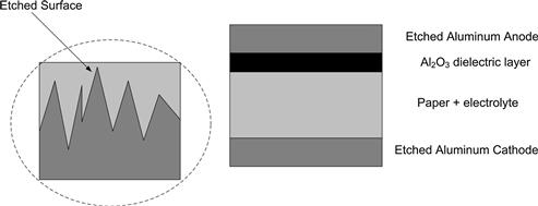
FIGURE 3.19 Electrolytic capacitor construction
The electrodes are normally etched to increase their effective surface area and so increase the capacitance per unit volume, hence modern electrolytics are sometimes known as “etched aluminum”. Because the electrolyte is an ionic conductor the polarity of the applied voltage must not be reversed, or hydrogen will be dissociated at the anode and create a destructive overpressure. The thickness of the Al2O3 dielectric is determined by the applied voltage during the electrochemical forming process, and to avoid further thickening of the dielectric during use (again with destructive results) the operating voltage must be kept below this voltage by a suitable safety factor, which determines the rated voltage of the component. Some manufacturers may specify a “surge” voltage rating, which is effectively the forming voltage without a safety factor.
Solid aluminum electrolytics are a variant in which the cathode is formed from a manganese dioxide semiconductor layer, contacted by an etched aluminum electrode. Although in principle some reverse polarization is possible with this system, it is not recommended because some ionic reactions due to trapped moisture can still occur.
Leakage
The important electrolytic characteristics tend to be dependent on application, and two broad areas can be discussed: for general purpose coupling and decoupling, and for power supply reservoir purposes. In the first field, the most important factor is usually leakage current, which becomes especially critical in timing circuits where it will determine the maximum achievable time constant. Leakage currents for general-purpose components are usually between 0.01 CV and 0.03 CV μA where C and V are the rated capacitance and working voltage. Many manufacturers offer low leakage versions which are usually specified at 0.002 CV μA. Alternatively, leakage current is a fairly well-defined function of applied voltage and usually drops to around a tenth of its rated value at about 40% of rated voltage, so that a low-leakage characteristic can be obtained by under-running the component. Leakage is also temperature-dependent and can be ten times its rated value at 25°C when run at maximum operating temperature. It is also a function of history (see section on Temperature and lifetime below): when voltage is first applied to a new component its leakage is higher.
Ripple current and ESR
For power supply reservoir applications, leakage current is unimportant and instead two other factors must be considered: ripple current (IR) and equivalent series resistance (ESR). The ripple current is the AC current flowing through the capacitor as the reservoir charges and discharges, usually at 100/120 Hz for AC mains supplies or at the switching frequency for switch-mode supplies. It develops a power dissipation across the resistive part of the capacitor impedance (ESR) which results in a temperature rise within the capacitor, and it is this dissipation which limits the capacitor’s IR rating. Published data for all electrolytics include an IR rating which must be observed. The rating increases to some extent with increasing frequency and reducing temperature. But note that the rating is normally published as an RMS value, and actual ripple waveforms are often far from sinusoidal, so a correction factor must be derived for this difference.
Such thermal considerations imply that, particularly for reservoir applications, you may need to select a capacitor with a higher voltage or capacitance rating than would be expected from the circuit parameters.
The ESR value (Figure 3.20) is important both because it contributes to the IR rating and because it limits the effective high-frequency impedance of the capacitor. This point has become of increasing importance with the advent of high-frequency switching power supplies, where the output ripple voltage is determined by the output capacitor’s ESR rather than its absolute capacitance value. Some manufacturers now offer special low-ESR versions specifically for these applications. ESR of non-solid electrolytics increases dramatically as the operating temperature is reduced below 0°C, which can be a problem in circuits where actual dissipation is low. The better-quality ranges of electrolytics include this factor in their specification of “impedance ratio”, the ratio of ESR at some sub-zero temperature to that at 20°C, which is usually around 3 or 4 but may be much worse. Solid electrolytics do not exhibit this behavior to the same extent.
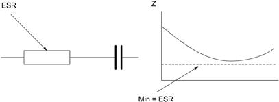
FIGURE 3.20 Capacitor equivalent series resistance
Temperature and lifetime
The capacitor characteristics as discussed for ceramic and film types are generally worse for electrolytics. Capacitance/temperature curves are rarely published but non-solid types can vary non-linearly by around ±20% over the operating temperature range, capacitance reducing with lower temperatures; solid types are better by a factor of two. Tan δ is around 0.1−0.3 at 100 Hz and 20°C but worsens dramatically with lower temperature and increasing frequency, higher voltage ratings having lower tan δ. Temperature ranges are typically −40°C to 85°C, with some types being rated for extended temperatures of –55°C to 105°C or 125°C. Lifetime is an issue with electrolytics, in two respects. Non-solid electrolytics suffer from eventual drying-out of the electrolyte, which is a function of operating temperature and the integrity of the component seal. In general, the life of these types can be doubled for each 10°C drop in operating temperature. Solid electrolytic types do not show this failure mechanism.
The second problem is that of shelf life. Non-solid aluminum electrolytics are one of the few types of electronic component that degrade when not in use. The dielectric Al2O3 film can deteriorate, leading to increased leakage, if the component is maintained for long periods without a polarizing voltage. The effect is dependent on temperature and shelf life is usually measured in years at 25°C. Capacitors that have suffered this type of degradation can be “re-formed” by applying the forming voltage across them through a current limiting resistor, if this is found to be necessary. At the same time, it is inadvisable to run this type of electrolytic in circuit configurations where it is not normally exposed to a polarizing voltage. Products which are likely to have been stored for more than one or two years before being switched on should be designed to tolerate high leakage currents in the first few minutes of their life.
Size and weight
One disadvantage of aluminum electrolytics is that they are often the largest and heaviest components in the circuit, with a few exceptions such as transformers. This means that they are a weak point when the assembly is vibrated. Some care should be taken in choosing the right part not only for its electrical characteristics but also for the mechanical strength of its terminals, if these are the only means of attachment; or in providing alternative means of mounting.
3.3.5 Solid tantalum
Solid tantalum electrolytics are generally used when the various performance, construction and reliability limitations of aluminum electrolytics cannot be tolerated. The construction is similar to the solid aluminum type, with a manganese dioxide electrolyte and sintered tantalum powder for the anode. They can be supplied with a temperature range of −55°C to 85°C or up to +125°C, and have a very much greater reliability than aluminum, and so are favored for military use.
Leakage current is around 0.01 CV μA which is comparable to the better aluminum types, and tan δ is between 0.04 and 0.1, about twice as good as aluminum. Capacitance change with temperature can vary from ±15% to as good as ±3% across the working temperature range. Some proportion of the working voltage can be tolerated in the reverse direction, which relaxes the application constraints. The resin-dipped bead tantalum construction offers usually the best trade-off between price, performance and size in a given application, and tantalum beads are available from a wide range of manufacturers.
Tantalum chip capacitors
A major advantage of tantalum capacitors is that they can be packaged in much smaller sizes than aluminum electrolytics. This means that they are better suited to surface mount production and indeed the majority of small SM electrolytics are tantalum types. Capacitance values from 0.1 μF to 470 μF are available.
One unusual problem does affect these components: tantalum is a rare material and there have been supply problems, compounded by their popularity, resulting in quoted lead times being pushed out to half a year or more. For this reason some designers look on tantalum capacitors unfavorably and try to minimize their use, or at least make sure they have multiple sources available for the chosen types. A newer material, niobium oxide, is offering itself as an alternative to tantalum and does not suffer from these supply problems, though its electrical characteristics are slightly less attractive.
3.3.6 Capacitor applications
As with resistors, the actual capacitance that a component can exhibit is only mildly related to its marked value. The art of circuit design lies in knowing which components must be carefully specified and which can have wide tolerances.
Value shifts
The actual capacitance will vary with initial tolerance, temperature, applied voltage, frequency and time.

Take a nominally 0.1 μF Z5U multilayer ceramic capacitor, rated at 50 V. It has an initial tolerance of −20%,+80%; a temperature coefficient of +22%, −56% max. over the temperature range +10 to +85°C; a capacitance voltage coefficient that reduces by 35% of its value at 60% of rated voltage; a frequency characteristic that reduces capacitance by 3% of its value at 10 kHz and 6% at 100 kHz; and an aging characteristic that reduces its value by 6% after 1000 h. It is run in a circuit with an operating frequency between 10 kHz and 100 kHz, over its full temperature range, and with an applied voltage that varies from 5 V to 30 V. The worst case limits of its actual value will be:


In other words, an 11:1 variation. Where is the 0.1-μF capacitor now? At the very least, you can see that it is most unlikely to be 0.1 μF!
Now repeat the calculation for a 10% polycarbonate component of the same value and 63 V rating, which will be larger; and a 20% tantalum bead electrolytic rated at 35 V, which will be roughly the same size but polarized. All three types are roughly the same price.
Polycarbonate:


Tantalum bead:


The polycarbonate performance is dominated by its initial tolerance; the tantalum bead shows a worse performance at the higher frequency. Clearly some 0.1 μF types are better than others!
The circuit conditions quoted above are fairly extreme, particularly the wide voltage range and the frequency excursions. But there are some applications where the subtleties of capacitor behavior have a serious effect on circuit operation. Consider the simple op-amp integrator.
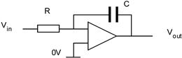
The output voltage follows the law:
![]()
Usually you will assume that C and R are constant and so if Vin is also constant the output ramp is linear with time. But if the integrator output swings over a wide range, say the 5–30 V considered in the last example, C may not be constant but will change as the voltage across it changes. This effect is most marked in accurate timing circuits or in circuits where a linear ramp is used to measure another voltage, such as in some A–D converters. A Z5U ceramic will introduce an enormous non-linearity; even X7R will have a poor showing.
The effect is best combated by choosing the proper dielectric type and/or under-running it, i.e. using a 100-V rated capacitor with no more than a 1-V ramp. Plastic film would be a better choice, polycarbonate being the preferred type for tempco and frequency stability, and would introduce negligible non-linearity.
NP0/COG ceramic, polycarbonate, polystyrene and polypropylene in roughly that order are most suitable for any circuit which relies on the stability of a capacitor, especially timing, tuning and oscillator circuits, as their capacitance values are least subject to temperature and aging. Of course, these types are restricted to the lower capacitance ranges (pF or nF − only polycarbonate stretches up to the μF range, and here size is usually a problem) and so are more suitable for higher frequencies. If long, stable time periods are needed it is normally better to divide down a high frequency using a digital divider chain than it is to use large-value capacitors, or to expect stability from an electrolytic.
3.3.7 Series capacitors and DC leakage
Capacitor voltage ratings can hide pitfalls. As discussed earlier, it is always better to under-run the working voltage of a capacitor for reasons of reliability. If a particular working voltage is just too high for the wanted capacitor type, it may seem reasonable to simply put two or more capacitors in series and add up the overall voltage rating accordingly, always taking into account the reduced total capacitance.
This is certainly possible but more is required than just multiple capacitors. The capacitor equivalent circuit (Figure 3.17) also includes the DC leakage resistance Rdc of each capacitor, as shown in Figure 3.21. The DC working voltage impressed across the terminals is divided between the capacitors not by the ratio of capacitance, but by the ratio of the two values of Rdc. These are undefined (except for a minimum) and can vary greatly even between two nominally identical components. Because Rdc is usually high, of the order of tens to thousands of megohms, other leakage resistance factors − particularly PCB leakage (see Section 2.4) − will also have an effect. The result is that the actual voltage across each capacitor is unpredictable and could be greater than the rated voltage. The problem is at its worst with electrolytics whose leakage current is large and varies with temperature and time.
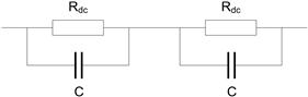
FIGURE 3.21 DC leakage resistance
The situation is to a certain extent self-correcting because an overvoltage will in most cases result in increased leakage which will in turn reduce the overvoltage. The major consequence is that the actual capacitor working voltage will be unpredictable and therefore reliability of the combination will suffer. Once one component goes short-circuit the other (or others) will be immediately over-stressed and rapid failure of all will follow.
Adding bleed resistors
The solution is simple and consists of placing resistors across each capacitor to swamp out the DC leakage resistance (Figure 3.22). The resistors are sized to be comfortably below the minimum specified leakage resistance so that variations in working voltage are kept below the rated maximum for each capacitor. Naturally this increases the leakage current of the combination but this is often an acceptable price, particularly if the application is for a high-voltage reservoir where some extra drain current is available.
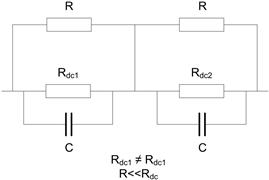
FIGURE 3.22 Swamping leakage resistance
Indeed, it is often necessary for safety reasons to have a defined “bleed” resistance across a high-voltage reservoir capacitor. If the load resistance is very high, it can take seconds or even minutes for the capacitor voltage to discharge to a safe level after power is removed, with a consequent risk of shock to repair or test technicians. A bleed resistor (or resistors, if the voltage rating of a single unit is inadequate) is a simple way of defining a maximum discharge time to reach a safe voltage.
3.3.8 Dielectric absorption
Another effect mentioned earlier is the phenomenon of dielectric absorption. If a capacitor is charged to a given voltage, discharged by shorting it, and then open-circuited again, its voltage will begin to creep up from zero towards the original voltage. The capacitor exhibits a “voltage memory” because the dielectric molecular dipoles need time to align themselves in an electric field.
This effect is of most concern to designers of sample-and-hold circuits. If a capacitor has been holding a voltage VA, and then samples another voltage VB at the other end of its range, when returned to hold mode (effectively open-circuit) its voltage will drift exponentially towards the old voltage VA (Figure 3.23).
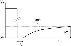
FIGURE 3.23 Dielectric absorption drift characteristic
The effect can be modeled by an extra circuit in parallel with the main capacitor, RdCd in the equivalent circuit (Figure 3.17). RdCd has a long time constant and transfers charge slowly to C when the capacitor is open-circuit. The dielectric absorption figure, quoted for t >> ts, is ΔV/VA − VB. The error due to dielectric absorption in a typical circuit will be reduced if the hold time of the old voltage (VA) is short, or if the measurement is made just after the sample is taken rather than many multiples of ts later. At the same time, selection of capacitor type plays a part, and of the readily available dielectrics polystyrene and polypropylene are the best, exhibiting dielectric absorption factors of 0.01−0.02%.
3.3.9 Self resonance
When capacitors are used at high frequencies another factor comes into play, and this is their self-resonant frequency (SRF). The capacitor equivalent circuit includes the ideal capacitance C, the equivalent series resistance and the equivalent series inductance (ESL). These three components form a low-Q series tuned circuit whose impedance versus frequency curve has the characteristic shape of Figure 3.24, showing a minimum impedance at self-resonance.
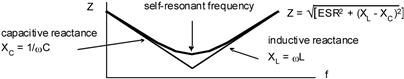
FIGURE 3.24 Capacitor self-resonance
The term “high frequency” here is relative. All capacitors exhibit the same basic curve, but the minimum for say a 47 μF tantalum electrolytic could be at 500 kHz and the null could be very flat, or for a 100 pF COG chip ceramic the null could be at 100 MHz and very well-defined.
The ESL is determined by the lead length and the body size. (Lead length includes the lengths of connecting pc track to the adjoining circuit nodes.) Therefore small, leadless chip capacitors show the lowest inductance and highest self-resonant frequency while large, leaded capacitors have high inductance and low SRF. Many manufacturers publish impedance/frequency curves if they expect their components to be used at high frequencies. A typical comparison, comparing small polyester film, tantalum electrolytic and multilayer ceramic of the same value, is shown in Figure 3.25.
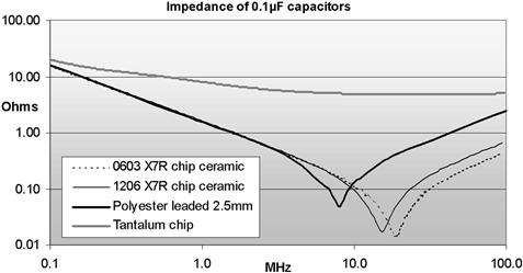
FIGURE 3.25 Impedance–frequency characteristics for plastic, ceramic and tantalum 0.1 μF capacitors
Consequences of self-resonance
A capacitor used above its self-resonant frequency is effectively a low-Q inductor and so RF circuits using inappropriate components can show somewhat unpredictable behavior. The problem also appears more frequently as the speed of digital circuits increases, and the clock frequencies approach or exceed the SRF of the capacitors that are used for supply rail decoupling (cf. Section 6.1.4). Clearly a tantalum electrolytic with an SRF of 1 MHz is not much use for decoupling clock transients of 10−20 MHz, but you can parallel large-value electrolytics with small-value, e.g. 10 nF, ceramic or film capacitors whose SRF is in the 10−100 MHz region. The combination is then effective over a much wider range of frequencies, and the technique is common practice in wideband amplifier circuits, although you need to beware of inter-component resonances, where, for instance, the high-value component’s self inductance resonates with the low-value capacitance.
3.4 Inductors
Hardly surprisingly, the inductor equivalent circuit (Figure 3.26) is very similar to the capacitor’s. All practical components contain the three passive circuit elements, R, C and L, in their makeup. Both capacitors and inductors are fundamentally energy storage devices, but the practical inductor departs further from the ideal than does the practical capacitor, and so is less universally used. Also, off-the-shelf inductors are less common than capacitors, and the prospects for multiple sourcing are slight.
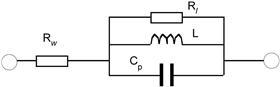
FIGURE 3.26 The inductor equivalent circuit
L is the “ideal” inductance of the device
Rw is the series resistance due to the winding wire and terminations, increasing with temperature
Rl is an equivalent parallel resistance due to the magnetic core losses, and is variable with frequency, temperature and current
Cp is the self-capacitance of the winding, determined by the method of construction of the component
Rw and Rl may be lumped together into an equivalent series resistance Req, in which case the overall lossiness of the component is quoted as its Q, which is given by ωL/Req. The reciprocal of Q is tan δ, which is analogous to the capacitor tan δ.
For this reason a tabular survey like those already given for resistors and capacitors is not really feasible. Inductors are generally made by winding wire around a magnetically permeable material and it is the performance of the material, along with the DC resistance of the wire, which determines the performance of the finished component.
3.4.1 Permeability
Permeability is the measure of a material’s ability to concentrate lines of magnetic flux. Air (and other non-magnetic materials) has a relative permeability, μr, of 1. Inductors wound on a non-magnetic core are inherently low-loss, the only losses being due to the wire resistance. Unfortunately they are also inherently low inductance, which generally limits their use to the HF and VHF regions. Achieving an inductance greater than 100 μH without a magnetic core requires a large number of turns, so that either the component becomes unmanageably large or the wire becomes unmanageably thin. At low frequencies the winding resistance approaches the inductive reactance, making the coil practically useless. Large air-cored coils do have applications where a stable, low-loss inductance is needed in the presence of high DC currents.
Most inductors for low- and mid-frequency use call for higher values, and must use permeable cores to achieve this. Relative permeabilities of several thousand are possible, allowing small inductors of several henries to be wound fairly easily. However, there are disadvantages, as you might expect:
• high-μ materials introduce losses of their own, reducing achievable Q factors;
• the materials reduce in permeability as the magnetic field increases. This is known as “saturation”, and means that the inductance drops off at high power levels or bias currents;
• a slight change in the material’s molecular structure on magnetization results in “hysteresis”, which shows itself as a remanent magnetic flux when the magnetic field reduces to zero, depending on the level of previous magnetization;
• the absolute magnetic and physical properties of the core are hard to control closely, so that the tolerance on the inductance value of the finished component is wide, though this can be controlled by an air gap in the magnetic circuit;
• the permeability and loss vary with temperature; above the “Curie point” the magnetic properties vanish almost completely.
Figure 3.27 shows a typical curve of magnetic flux versus applied magnetic field (the “B–H” curve) for a ferrite material, illustrating the effects of saturation and hysteresis. You will use such published curves in inductor design, primarily to determine the power-handling capability of the component.
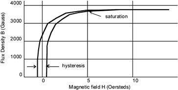
FIGURE 3.27 Typical B–H curve for a ferrite
Ferrites
The properties of permeable cores are reminiscent of the dielectric characteristics − variability with voltage, temperature and frequency − of the hi-K ceramics that we looked at earlier, and indeed there is much in common. The most common core material, ferrite, is in fact a type of ceramic, and is produced in at least as many varieties as are the capacitor ceramic materials. Ferrites are a metal-oxide ceramic made of a mixture of Fe2O3 and either manganese–zinc or nickel–zinc oxides pressed or extruded into a range of core shapes. Every manufacturer offers a wide variety of shapes and will usually also offer a custom service for large volumes, but for most uses a selection from a relatively small range of standard types is adequate, and offers the benefit of sourcing from different suppliers. Two of the most popular core types are the RM series to IEC 60431 and the E, EP and EC series for medium-power high-frequency transformers.
Manganese–zinc ferrites have a high permeability but also their losses increase rapidly with frequency, making them more suitable to low-frequency applications. Nickel–zinc ferrites are of lower permeability, but their lower high-frequency losses make them useable up to about 200 MHz. Their resistivity is higher by several orders of magnitude, and their Curie point temperature is higher. The ratio of manganese to zinc or nickel to zinc in either case determines the grade of material.
The use of the terms “hard” and “soft” when applied to magnetic materials does not refer to their physical hardness but to their coercivity (although there is a correlation and is in fact where the term comes from originally). Soft magnetic materials are generally defined to have coercivity less than 1 kA/m and hard magnetic materials greater than 10 kA/m. Ferrites are chemically inert ceramic materials which have the general structure XFe2O4 where X is one of the transition metals given in Table 3.6.
Table 3.6 Transition Metals for Magnetic Materials
| Metal | Symbol |
| Manganese | Mn |
| Zinc | Zn |
| Nickel | Ni |
| Cobalt | Co |
| Copper | Cu |
| Iron | Fe |
| Magnesium | Ma |
Combinations of powders of these metals are then mixed according to specific proportions, milled to ensure the required grain size and then pressed into shape. Sintering, heating to between 1150°C and 1300°C, hardens the material physically and ensures the desired magnetic properties. The sintered core may still require further finishing, ensuring accurate dimensions or smooth surfaces for mating core halves, and if so the material is finely ground. This grinding is also used to accurately implement center core air gaps.
The sintered and finished material contains thousands of small crystals or grains of the ferrite material, usually tens of μm across. Figure 3.28 shows a scanning electron microscope image of a soft ferrite material magnified 2500 times, illustrating the shape and size of the grains in the material. Each grain has one or more magnetic regions, called domains, that are already randomly magnetically oriented due to the material’s intrinsic magnetization after heating. These domains come into progressive alignment with the application of an external magnetic field as shown in Figure 3.29.
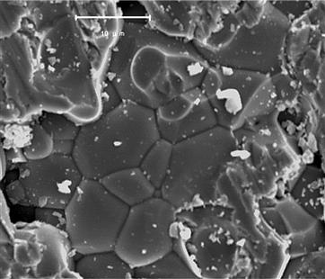
FIGURE 3.28 Scanning electron microscope (SEM) image of Philips 3F3 soft ferrite material with a magnification of 2500 showing ferrite grains
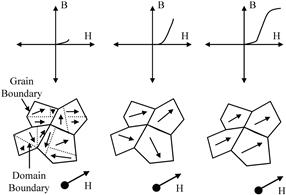
FIGURE 3.29 Progressive alignment of magnetic domains and grains, and the resulting magnetization curves for applied field strength H
Iron powder
The other core material in wide use is iron powder. Such cores are pressed from a very fine carbonyl iron powder mixed with a bonding material. Eddy current losses in the core are minimized by creating an insulating layer on the surface of each particle before pressing, but this introduces minute gaps in the magnetic circuit, which restricts the permeability of the material to a maximum of around 30. The same effect makes iron powder cores very hard to saturate. The main uses for iron powder are for high-frequency tuned circuit cores, and suppressor chokes where low saturability is more important than high inductance.
3.4.2 Magnetic material definitions and metrics
In order to assist in the definition of appropriate magnetic materials and components it is important to define the requirements. It is quite normal to classify the differences between materials simply using the overall major loop characteristics, but it is also important to consider specific metrics, such as remanence or coercive force. The behavior of smaller loops, called minor loops, is significant for wide-band transformers. The accurate characterization of the energy loss is critical for energy conservation and power calculations, especially with arbitrary applied fields. With the use of specific metrics clear distinctions can be drawn between materials and their equivalent models under any applied field conditions. In this section, the important aspects of the behavior of magnetic material hysteresis are defined. Metrics are also specified for the measurement of, and comparison between, different materials and material models.
Hysteresis loop definitions
In order to understand the different requirements of magnetic models it is useful to distinguish between different types of hysteresis behavior in magnetic materials. The basic types of magnetization curves are shown in Figure 3.30.
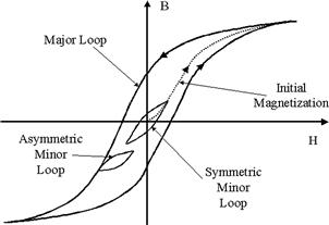
FIGURE 3.30 Types of magnetization curve and hysteresis loop
The major loop is the magnetization curve when the applied field (H) is high enough to force the material into saturation and the B–H loop closes at the tips. The initial magnetization curve is the transition of the flux density (B) from the initial condition of zero flux to the tip of the major loop. Any loop inside the major loop is defined as a minor loop, and these may be asymmetric or symmetric about the origin as shown in Figure 3.30. It is obvious that for accurate simulation of an arbitrary applied field, the initial conditions of flux or magnetization in the model must be correct. The anhysteretic curve is that which the magnetization would relax to for any specific value of applied field (H). This is effectively the minimum state of energy and is shown in Figure 3.31.
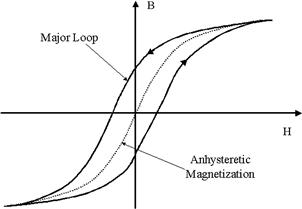
FIGURE 3.31 Anhysteretic magnetization curve
When considering the minor loop behavior of magnetic materials, it is necessary for a model to be capable of exhibiting non-congruency. This means that the minor loop shape changes depending on the initial flux level.
Hysteresis loop metrics
It is possible to compare the performance of magnetic materials using numerical methods such as the least squares approach, however, it is more useful to compare standard measured characteristics and use them as metrics which define the performance of the material and allow better classification of the materials. Figure 3.32 shows a basic set of the metrics for a major hysteresis loop. The definitions of the metrics are given in Table 3.7.
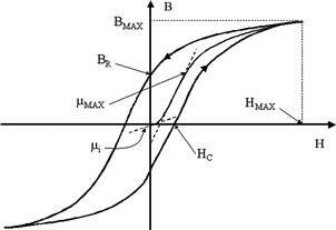
FIGURE 3.32 Major B–H loop showing basic set of metrics
Table 3.7 Definition of Magnetic Material Metrics
| Metric symbol | Metric definition |
| BR | Remanence – B axis crossing point |
| HC | Coercive force – H axis crossing point |
| BMAX | Maximum flux density |
| HMAX | Maximum applied field |
| μMAX | Maximum permeability |
| μi | Initial permeability |
While these metrics are straightforward to measure directly from a B–H curve, there are other metrics which are also of use including the area of the B–H loop. This defines the energy lost per cycle and in conjunction with the frequency can be used to estimate the power lost by the material. Examples of the estimated power loss for a range of materials can be found in typical manufacturer’s data. The maximum permeability μMAX can refer to the maximum initial permeability (as shown), the maximum incremental permeability (when a small AC signal is applied on top of a DC offset signal and the permeability measured), or the maximum effective permeability (measured at the extremities of the B–H loops).
Leakage inductance
When a magnetic component is constructed from a number of windings and a core, the main design aim is usually to maximize the magnetic flux through the core, as this allows maximum energy transmission from winding to winding and the maximum inductance from the component. Unfortunately, not all the flux passes through the core and the flux that passes through the windings themselves, or the winding space, is called the leakage flux. This flux gives rise to an inductance which is called the leakage inductance. Figure 3.33 shows a simple two-winding transformer with the ideal and leakage flux paths defined.
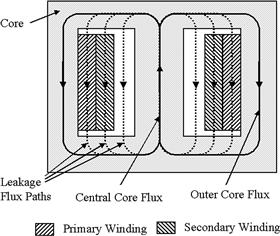
FIGURE 3.33 Flux paths showing leakage flux
The leakage inductance can be a vitally important parameter in switching power systems as it can give rise to resonance and ringing effects – causing losses. Equally leakage inductance can cause problems with line transformers, as this parameter is crucial in defining the bandwidth attainable for a transformer.
Measurement methods
The standard method for measuring leakage inductance of magnetic components is based on the fact that if a winding is shorted, the field applied by another winding will then be automatically cancelled out by the opposite field generated by the shorted winding (this is the assumption, but in practice the mutual flux is not cancelled out completely). The IEEE standard practice for the measurement of leakage inductance using this method is given in IEEE Recommended Practice for Testing Electronic Transformers and Inductors, IEEE Std 389-1996.
In practice the simplest method is to short the secondary winding(s), and measure the inductance across the primary winding using either an inductance bridge, or an impedance analyzer. It is important to ensure that measurements are taken across the frequency range of interest and at a low signal level to reduce the effect of core saturation reducing the effective inductance.
Numerical methods
The use of finite element analysis to calculate the leakage inductance in transformers is in some ways even more accurate than measuring using the shorted winding approach described previously. In a finite element analysis, it is possible to define the applied fields so that the mutual flux is exactly zero, thus ensuring maximum accuracy of the calculated leakage inductance. The accuracy of the calculated value is primarily affected by the numerical accuracy in the basic finite element analysis, and any approximations made in the construction of the model.
The procedure is to apply the equal and opposite fields to the windings to make the mutual flux zero. This is obviously straightforward in the finite element analysis software as the applied winding currents can be specified exactly, and from the resulting energy stored in the finite element model, the leakage inductance can be directly calculated.
Issues with unusual winding configurations
Multi-wire, interleaved and split bobbin windings present a more difficult problem. In these cases, instead of the winding consisting of an integral number of turns in a single section of the winding area, the winding topology may be much more complex. Multi-wire windings are where more than one wire is wound together to create a winding. For two wires this is bi-filar, three wires tri-filar and so on. Split bobbins are used to divide the winding area into lateral regions so that windings can be placed side by side. Interleaving can occur in a variety of ways, but the basic approach is to split the individual layers of a windings and intersperse the layers with those of another winding. This approach is sometimes called sectionalized winding. The main reason for this method is to reduce leakage inductance. Figure 3.34 shows the configurations for a two-winding transformer with (a) a simple side by side arrangement, (b) bifilar windings, (c) split bobbin and (d) interleaving.
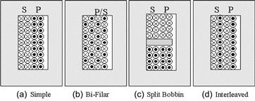
FIGURE 3.34 Simple, bi-filar, split bobbin and interleaved windings
3.4.3 Self-capacitance
Generally, don’t wind directly onto the core. Apart from mechanical instability, the very high dielectric constant of the ferrite will increase the self-capacitance Cp of the winding several times if the two are in close contact. The bobbin serves to keep the winding well spaced from the core and minimizes self-capacitance. The way the winding is built up also influences self-capacitance; a single layer has the lowest capacitance, but if multiple layers are necessary then two possibilities exist to reduce it:
• “scramble” or “wave” wind rather than build up in discrete layers. This can reduce Cp by around 20% over a layer winding, but uses more winding space;
• use a multi-section former for a single winding. Again this uses more space but, for example, a two-section former can reduce Cp by a factor of 3.
Generally the capacitances are not considered frequency- or temperature-dependent (i.e. the dielectric material is largely of a constant relative permittivity) within the range of interest of SMPS and communications components. This assumption cannot be made for higher frequency RF components however. It is also assumed for the purposes of calculation that the voltage across a winding is distributed evenly, proportional to the number of turns.
Measurement methods
The measurement of the winding capacitances of a transformer is not an easy task to perform, but can be carried out using the procedure defined in IEEE Standard 389-1979 for a two-winding transformer. More complex winding structures can also be measured using variations of this approach. The technique uses the resonant frequency of the transformer in various configurations to extrapolate the winding capacitances based on the equivalent circuit shown in Figure 3.35, and using separately obtained values for the inductive elements.
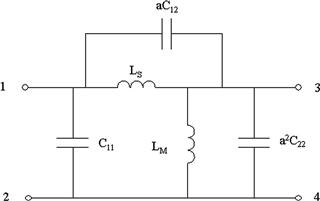
FIGURE 3.35 Equivalent circuit assumed for measurement of winding capacitance
3.4.4 Winding losses
Background
Losses in magnetic component’s windings occur for a variety of reasons. The wires have a finite resistivity which causes a DC resistive loss. This can be quite easily calculated from the resistivity of the wire and its dimensions. As the frequency of an applied signal increases eddy currents are generated inside the winding leading to further losses. These eddy currents occur in two forms: skin effect and proximity effect. The skin effect is a function of the frequency of the applied signal and is calculated easily. The effect occurs as the signal tends to flow nearer the surface of the conductor as the frequency increases. The second is the proximity effect of the conductor strands themselves. This is a result of eddy currents induced from the overall magnetic field, and is dependent on the wire layout, and whether stranding, twisting or bunching has taken place. This can be more difficult to calculate analytically as there may be a significant variation in the layout of the individual conductors.
Theoretical methods
The low-frequency resistance of a conductor can easily be calculated using the length of the conductor, the cross-sectional area, and the resistivity (for copper this is 1.709 × 10⁻⁸ Ωm). It is important to note that the resistivity is temperature-dependent. For copper the thermal coefficient is Tc = 0.00393 Ωm/°C. This is an important consideration for power devices where a 40°C temperature rise would not be uncommon. This approach can be used for a winding with N turns and a mean turn length lw to estimate the DC resistance as given below, where d is the diameter of the conductor and ρc is the conductivity.
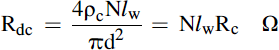
As discussed above, the losses due to eddy currents in windings can be divided into skin and proximity effects. As the frequency of an applied signal increases, the current flows in a progressively thinner layer at the surface of the conductor. Figure 3.36 shows the change in the penetration depth in a conducting copper wire at different frequencies. The thickness of this layer is called the penetration depth, denoted by Δ, and can be calculated using the equation below, where ρc is the resistivity of the conductor, μc is the relative permeability of the conductor and f is the frequency of the signal.
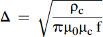
The skin depth is related to the conductor diameter d to obtain a relative measure of the skin depth that results in a “skin effect factor” F. If d/Δ is <2 then the skin effect is negligible and can be ignored. As Δ decreases, and d/Δ increases above 5 then the skin effect factor, F, can be approximated using
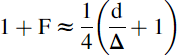
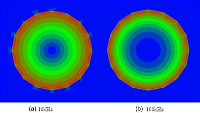
FIGURE 3.36 Variation in conductor skin depth with frequency
Measurement methods
In order to measure the winding losses, several steps need to be taken. The losses can be generally lumped into two parts: Rdc which is the DC winding resistance and Rac which is the frequency-dependent loss, comprising mainly the eddy current losses in the winding.
The Rdc measurement can be carried out easily using a measurement bridge or an impedance analyzer at very low frequency. The Rac measurement can best be carried out using an impedance analyzer, sweeping the frequency of the applied signal over the required range. The impedance and phase can be used to calculate the AC resistance, or the analyzer may output the real and imaginary parts directly. Care must be taken to ensure that low applied signal levels are used so that the core of the device under test is not saturated.
Proximity effect
With more than one winding in the component, the magnetic field in other windings causes eddy currents in the winding of interest and this is called the proximity effect. This is illustrated with the finite element analysis of two windings with currents flowing in the opposite directions shown in Figure 3.37. This shows the distribution of the magnetic field, and the current inside the conductors (the lighter shades indicate areas of high current density).
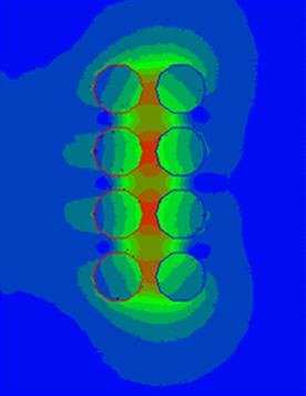
FIGURE 3.37 The effect of proximity on the magnetic field distribution in windings
This can be approximated for idealized winding structures leading to the expression for the power loss due to the proximity effect for round conductors given by:
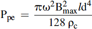
Further dependence on frequency in the form of a skin effect factor for this power loss is introduced similarly to the basic skin effect factor F, but this time alters the proximity effect. This factor, Gr, tends to unity for low frequencies, but as the ratio of d to Δ increases beyond 4, the factor takes the form shown in:
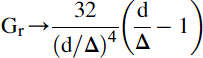
3.4.5 Inductor applications
There are three major applications for inductors: as frequency-determining components in tuned (resonant) circuits, as energy storage components, usually in power supplies, and as filter components in suppression circuits. Each application emphasizes different inductor characteristics and calls for a different approach to inductor design.
Tuned circuits
Signal-tuned circuits demand predictable inductance values and high Q (low losses). They do not normally see high bias currents, so core saturation and hysteresis loss is not a problem. For low frequencies, ferrite pot cores are the most popular, but for RF use (above 1 MHz or so) other types of ferrite core, or iron dust cores, are better. For the best stability and initial tolerance, a lower permeability material is preferable.
As well as the intrinsic stability of the material, for these applications it is important to consider mechanical stability. Any movement or distortion of the core, or movement of the winding relative to the core, will affect the magnetic path and hence the inductance. Also, any mechanical, magnetic or thermal shock to the core causes an immediate change in permeability followed by a long, slow relaxation towards the original value. This is known as “disaccommodation”. These effects mean that the core characteristics have to be very carefully considered when a stable inductance is required in a high-shock or high-vibration environment. It is common for the winding, bobbin and core to be encapsulated in varnish to enhance mechanical stability. Hard encapsulating compound should not be used as the high shrinkage could mechanically damage the brittle core.
Power circuits
Energy storage chokes and power transformers, as used for example in switching power supplies, have a quite different set of important parameters. In these, inductance stability is not required but high volumetric efficiency is. Energy stored in the choke is given by L × I2 and so a material which shows a high saturation flux density, allowing a higher magnetizing current, is to be preferred. At higher operating frequencies hysteresis becomes the dominant loss mechanism, and limits the power-handling capacity of the core. A small gap in the magnetic circuit, usually obtained by grinding away a part of the core, allows higher saturation at the expense of lower effective permeability. These considerations point to the use of gapped manganese–zinc ferrites or iron dust cores in which the air gap is inherent in the material.
Suppression
In contrast to the previous applications in which low core losses were required for high Q or high power handling, suppression chokes work best if they have high losses. A suppression circuit has to reflect or absorb high-frequency interference energy and prevent it from being propagated beyond the suppressor. The more energy is absorbed within the choke the better will be its circuit performance. Clearly, high-loss ferrites are the best type for these applications; all ferrites when used well above their intended frequency range exhibit high losses, but materials specifically designed and characterized for this purpose are available. The ferrite bead (Figure 3.38) is an extreme example, in which a straight piece of wire is transformed into a high-frequency choke merely by stringing a bead onto it. The losses induced in the ferrite at high frequencies give the assembly a complex impedance (resistance + reactance) of several tens of ohms. The same principle is applied to monolithic ferrite chip components, in which the conductor is passed between layers of ferrite to create a surface mount part.
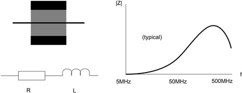
FIGURE 3.38 The ferrite bead
3.4.6 The danger of inductive transients
One of the fundamental circuit laws pertaining to inductors is the relationship
![]()
This says, in effect, that the voltage across an inductor is proportional to the rate of change of current through it, and it is the basis for an enormous number of unreliable circuit designs.
Consider a simple circuit: an inductor in series with a resistor and a switch, connected to a DC voltage source, as in Figure 3.39.
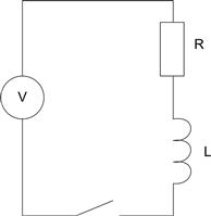
FIGURE 3.39 Series inductor-switch circuit
When the switch is closed, the current through the inductor will build up according to the above equation until it is limited by R to the steady-state value of V/R. So far so good. But what happens when the switch opens?
The current through the inductor is cut off instantaneously with nowhere to go. But this means that di/dt is infinite. So, according to the equation, should be the voltage across it. And this is indeed what happens; at the instant of switch-off, a large voltage transient is induced across the inductor. In practice, its amplitude is not infinite but is determined by the Q and the self-capacitance of the inductor, which forms the only path (apart from leakage) for diversion of the stored current. Or, if the self-capacitance is small and the transient is large enough, its amplitude is limited by breakdown across the switch. This is the source of the unreliability of any circuit design which uses this configuration, of which there are many. (It is also the principle of operation of the car ignition circuit, of which there are millions.) As an example, consider the relay coil.
Relay coils
A typical relay drive circuit has the coil driven by a transistor switch (Figure 3.40). The waveform seen at A on switch off is a damped sinusoid that has a high initial value but dies away rapidly. The equivalent circuit of the relay coil is an RLC tuned circuit where the R, L and C values are the winding resistance, inductance and self-capacitance respectively. The period of the damped oscillation is determined by the L–C resonant frequency, and the amplitude and decay time constant of the waveform are determined by the Q of the circuit, i.e. by R , L and C. The resistance of a relay coil is always specified by its manufacturer; the inductance is sometimes specified, the self-capacitance never. So the only way to determine the peak value of the transient is to measure it in circuit.
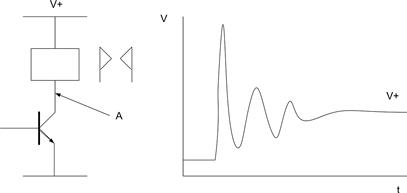
FIGURE 3.40 Relay driver and turn-off waveform
Transient amplitudes of several times the supply voltage are common. It is quite possible to get transients of hundreds of volts from a 12-volt supply, as automotive electronics designers know only too well. If the transistor switch has a collector-emitter breakdown voltage less than the transient peak, the transistor will suffer avalanche breakdown and the transient will be limited. Transistors can withstand repeated low-energy avalanche breakdowns before failure and so, if the circuit is not fully investigated, it will appear to work quite satisfactorily on the bench; it will only be after some time in the field that a high incidence of transistor failures will be noticed. By that time, the product’s reputation for unreliability has been established.
This problem is not limited to transistor drive circuits. There are many applications where a small switching contact is driving a larger switching coil, for example a reed relay driving a larger relay, or a large relay driving a contactor. The same inductive spike phenomenon will lead to spark erosion of the low-power switching contacts, and early failure, if it is not prevented.
Transient protection
Unfortunately, all protection methods involve extra components. Each method seeks to divert away the energy-storage current from the inductor without creating a large transient voltage. The diode method of Figure 3.41(a) is the simplest and often the best. It clamps the positive-going spike to the supply rail, and for all practical purposes limits the positive voltage seen by the switch to that of the supply. The diode need only be sized to withstand the surge of flyback current limited by the coil resistance, and its voltage rating need be no more than the supply. This circuit does, though, lengthen the turn-off time of the coil, since the stored inductive current continues to flow through the diode for a short time after the switch is opened, and this may limit its applicability.
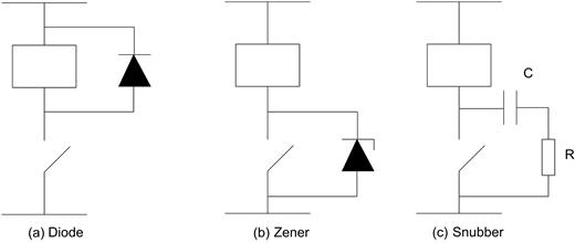
FIGURE 3.41 Inductive transient protection
Protection against negative transients
The single diode clamp does not protect against a negative-going transient that drives the switch voltage below the 0 V rail. This can be prevented by including another diode in series with the switch, or by the zener circuit shown in Figure 3.41(b). The zener clamps both negative and positive transients, but its positive clamping action is somewhat less effective than the single diode. This is because its specified breakdown voltage must ensure that worst-case tolerances on supply voltage and zener voltage do not result in continuous conduction, and so the actual clamping voltage is inevitably higher than optimum. This is not usually a problem unless the breakdown voltage of the switch is already close to the supply voltage, which is bad practice anyway. The zener has the additional advantage of protecting the switch against transients on the supply rail. It can also be sized to achieve a compromise with respect to the turn-off time of the coil.
AC circuits
Both the diode and zener methods are only applicable when the supply is a polarized DC voltage. An AC coil requires a different protection method, and for this the snubber circuit Figure 3.41(c) is used. This essentially places an RC network in the path of the inductive current − the network can equally well be across the switch or the coil, provided the supply impedance is low − so that the current is absorbed by the action of charging C. The C is effectively in parallel with the self-capacitance of the coil which it swamps. The resistor limits the switch current when C is discharged at turn-on.
In this circuit, C should be sized carefully to ensure it is no greater than required to reduce the transient to a manageable level, since it slows down the response of the switch and also allows some current into the load when the switch is open. Similarly, R should be kept as high as possible, consistent with the snubbing action since power is lost both in it and in the switch, as C is discharged. The snubber is a popular network both for AC inductive clamping and in many other circuits as a dV/dt limiter. Calculation of snubber values is outlined in Section 4.2.6.
3.5 Crystals and resonators
The quartz crystal has been widely used as a frequency-determining component for many years. It is small, robust, accurate and stable. Also, like other components, it has its vices. This section will look briefly at crystal theory before reviewing some application pitfalls, and also cover its cheaper but more popular cousin the ceramic resonator.
Quartz (silica, SiO2) exhibits a piezoelectric effect whereby mechanical stress generates a directionally related electric field, and conversely an applied electric field causes a directionally related force across the crystal. An alternating voltage applied to the crystal will cause it to vibrate, and if its frequency is close to the mechanical resonance the generated electric field will be amplified and can be used to stabilize the applied frequency.
Angle of cut
The crystals used in electronic circuits are in the form of plates or elements cut from a synthetic crystal. The resonant properties vary depending on the angle of cut referred to the base crystal’s major axis. X- and Y-cut units, where the direction of cut is perpendicular to the major axis, show subsidiary responses which can reduce the Q-factor of the element and impose a fairly low upper limit on the achievable frequency range. Also, the temperature coefficient of these cuts is large.
Happily, a particular angle of cut of 35° 21′ from the major axis known as the AT-cut, shows very small coupling between the principal and other modes of vibration, therefore lacks subsidiary resonances and is capable of very-high-frequency operation. Its resonant frequency is governed directly by a fraction of the element thickness, and its temperature coefficient follows a cubic-plus-linear law whose actual slope varies according to the deviation of angle of cut (see Figure 3.45). The AT-cut crystal is the most widely available crystal unit for general purpose use. Other cuts are available for specialized applications.
3.5.1 Resonance
The crystal equivalent circuit is a series LCR tuned circuit together with a parallel capacitance (Figure 3.42). C, L and R are functions of the mechanical resonance properties of the crystal element and Co is the static capacitance due to the electrodes and terminations. C is very low (of the order of femto-farads) and L is very high (of the order of henries), while R is generally tens or hundreds of ohms for high-frequency units, and the Q of the resulting combination is very high (30 000−100 000).
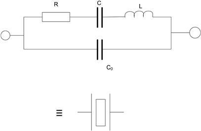
FIGURE 3.42 Crystal equivalent circuit
Because of this, the phase angle changes very rapidly with changes in frequency near resonance. So as an oscillator feedback component, the crystal will correct amplifier phase deviations with only a slight frequency shift.
Co is several hundred times larger than C, and is also increased by external circuit capacitance. The crystal shows two resonant modes, series and parallel, as Figure 3.43 indicates. Their resonant frequencies are very close together and are given by:
![]()
![]()
where Cx is the series combination of C and Cp, and Cp = Co + external capacitance.
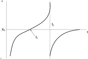
FIGURE 3.43 Series and parallel resonance
The crystal can be operated in either mode. In series mode, the element is operated at a low impedance which is equivalent to R; it can be “pulled” upwards in frequency slightly from fs by inserting external series capacitance. In parallel mode the element operates at high impedance and can be pulled downwards in frequency from fp by adding external parallel capacitance. The frequency shift from fs in either case is the same for a given external capacitance. Clearly, a given resonant frequency is only obtainable if the external capacitance is known, and in fact all crystals are supplied for a quoted “load” capacitance. The unit will only operate at the marked frequency (within the given tolerance) if the actual circuit capacitance is as specified. Conversely, the frequency can be trimmed if absolute accuracy is needed by using a variable load capacitance.
3.5.2 Oscillator circuits
There are two common circuits for digital clock oscillators (Figure 3.44), one operating in each mode. The parallel circuit is only suitable for high-impedance (CMOS) devices while the series circuit can be used for high- or low-impedance devices. The parallel circuit can be run at very low power levels (down to 1 μA) but is slow to start. It is commonly used by on-chip microprocessor clock oscillators and other CMOS oscillator/divider ICs, such as real-time clocks.
FIGURE 3.44 Typical crystal-based oscillators
Rf biases the inverter to linear operation and should be low enough for input bias current to have negligible effect but high enough not to load the crystal. Generally 10−15 MΩ is reasonable. The crystal appears primarily inductive and provides 180° phase shift in the feedback loop. C1 and C2 in series together with circuit strays (amplifier input and pc track capacitance, amounting to at most 10 pF with good layout) form the crystal load capacitance. The ratio C2:C1 should generally be of the order of 3:1, C2 being variable if frequency trimming is desired.
Drive level resistance
Ra is an important component and should not be omitted without proper consideration. It sets the drive level to the crystal. Too high a drive will lead to frequency instability and possible damage to the element. Too low a level will make the oscillator slow to start, perhaps impossible to start with low-activity units, and susceptible to interference. Typical AT-cut crystals have a maximum drive level of 0.5–1 mW. Some circuits (for example low-power on-chip CMOS oscillators) have a high enough output impedance to make Ra unnecessary but this is not normally the case with discrete-gate oscillators. For watch-crystal units (32.768 kHz) Ra should be tens or hundreds of kΩ.
Series circuit
Some applications may be embarrassed by the slow starting time (possibly up to 1 second) of the parallel oscillator circuit. Crystals have a very high Q and if the drive level is low, for frequency stability or to conserve current, the time taken to reach working level is appreciable. This may be unacceptable in microprocessor clock circuits where the clock is expected to be present immediately on power-up. For these purposes the series oscillator, in which the crystal is operated at a low impedance with minimal phase shift across it, is preferable. Its main disadvantage is its higher supply current. The same strictures on drive level apply. Note that the effective series resistance of the element, which is equivalent to its motional resistance R, can vary widely from unit to unit. A spread in this parameter of two- or three-to-one is not uncommon, so it is wise to design the circuit for assured start-up with a three times higher R than quoted.
Layout
Circuit board layout is important, particularly for the parallel mode. Extra capacitance across the crystal should be minimized, as this will increase loop gain and short-term stability. So should coupling between the oscillator circuit and other circuits, especially logic switching circuits, as this decreases the likelihood of spurious oscillation. Ground traces around the crystal to buffer other tracks are advisable; on no account route logic signals near or through the oscillator circuit as they will couple into the high-impedance nodes and cause frequency instability or jitter.
3.5.3 Temperature
Lastly, beware of temperature coefficients. The temperature law of the AT-cut is cubic (Figure 3.45) and if the cut angle is chosen carefully can be fairly flat at room temperature, but it worsens rapidly as the temperature limits are neared. A crystal will oscillate outside its rated temperature (usually) but the frequency stability will be impaired.
FIGURE 3.45 AT-cut frequency/temperature curves
(Source: ECM Electronics)
Tuning-fork crystals (the ubiquitous 32.768 kHz type, universally used for real-time clocks) show a parabolic curve, of around −0.04 ppm/°C2. The turnover temperature is around 25°C which means that for digital watch applications, where the wrist temperature remains around this value, it is ideal and very stable. Transfer this type of crystal to an industrial real-time clock (for example) and its timekeeping at the extremes of the range is hopeless: at +85°C, and at −35°C, it is 144 ppm low which represents a loss of 12 seconds per day. Be warned: use an AT-cut!
3.5.4 Ceramic resonators
A cheaper alternative to the quartz crystal is the ceramic resonator. This device uses the mechanical resonance of a piezoelectric ceramic, typically lead zirconate titanate (PZT), which vibrates in various mechanical modes depending on the chosen resonant frequency. The frequency ranges are approximately:
30 kHz–1 MHz: longitudinal mode
1 MHz–10 MHz: shear thickness mode
The equivalent circuit of the resonator is identical to that of the quartz crystal (Figure 3.42) but the component values give it orders of magnitude lower Q. In terms of oscillation frequency accuracy, the resonator sits between the quartz crystal and the LC resonant circuit. The tempco of a resonator is of the order of 10–5/°C compared to the better than 1 ppm/°C achievable with quartz, and the 10–3 to 10–4/°C of LC circuits. Its initial frequency tolerance is of the order of ±0.5% whereas quartz routinely achieves ±0.003%; to achieve these figures using LC circuits would need a trimming adjustment. On the other hand, the resonator is cheaper and smaller than quartz crystals, and can use the same or similar oscillator circuits.
Load capacitors as in Figure 3.44 are necessary to prevent spurious oscillation modes and the manufacturer’s recommendation for the oscillator circuit should be followed. A further advantage of the resonator is that because of its lower Q, the oscillation will start up more quickly than for an equivalent crystal circuit, which makes it attractive for applications which spend a lot of their time in “sleep” mode with the oscillator powered off.
All of these characteristics make the ceramic resonator the component of choice for frequency control of low- and mid-performance digital products, where a stable clock frequency is needed but where absolute accuracy or close control of tempco is not a requirement. It is mass produced and available in a wide range of standard frequencies, matched to particular consumer applications such as DTMF (telephone dialing tone) generators, remote control units, and TV and audio systems.