
Chapter 23. High-Performance Gate-Level Simulation with GP-GPUs
Debapriya Chatterjee, Andrew DeOrio and Valeria Bertacco
A successful, correctly functioning product is the goal of every semiconductor design. However, correctness is an elusive goal, complicated by ever-increasing complexity of hardware designs. This complexity is enabled by continually shrinking semiconductor technology, enabling designs that incorporate more and more components and functionality with each new generation. Verifying a complex chip is the most time-consuming process in the design flow, typically carried out through logic simulation, a computationally intensive process where the nascent design is tested for correct functionality. Logic simulation is traditionally run on large server farms of computers to counter its low performance and throughput. Unfortunately, protracted simulations, especially at the gate-level, significantly limit the portion of the design that can be verified. Improvements in simulation performance have great potential to boost verification capabilities, thereby decreasing the number of bugs in a design that escape into the final manufactured product. We approach this goal by leveraging recent GP-GPU technology, thus enabling massive parallelism in logic simulation. Our techniques enable large, complex designs to be mapped onto a GP-GPU leading to order-of-magnitude performance improvement and efficiency of current server farms.
23.1. Introduction
The vast complexity of modern semiconductor systems is challenging all aspects of their development. Among these, functional verification is the most critical one, absorbing more than 70% of the effort and resources of the entire development. Incomplete or limited verification leads to the discovery of functional errors (bugs), late in the development process, or aftermarket release of a silicon product. The impact of these bugs may lead to development delays, financial losses, and product recalls.
The majority of verification methodologies in industry rely heavily on the use of logic simulation tools. These tools simulate the design's functional behavior at different levels of abstraction, ranging from high-level behavioral to low-level structural gate-level descriptions. A typical simulation will rely on a model of the design, stimulating it with inputs and then checking the outputs for correctness. Unfortunately, this approach is very slow: even in the face of decades of improvements in the performance of these tools by the EDA industry, they still lack the horsepower required to tackle today's
complex digital designs, especially when simulating gate-level netlists, where the system's description is fairly detailed, leading to a large design model.
In a typical digital design flow, a system is first described in a high-level behavioral fashion with a hardware description language (HDL), then it is automatically synthesized to a netlist, consisting of structural logic elements such as logic gates and flip-flops. To ensure that the gate-level design provides the same functionality as the behavioral design, the former must be validated by thorough simulation and comparison with the behavioral model. These structural netlists can easily consist of tens of millions of gates in modern digital systems. A logic simulator takes this netlist as input, converting it to internal data structures: feedback loops are opened by disconnecting the sequential storage elements in the design, thus allowing to simulate the design one cycle at a time, storing the value of latches and flip-flops in internal data structures of the simulator software. The remaining logic, that is, the combinational portion, is then levelized according to the dependencies implied by the gates input-ouput connections. Simulation proper can now begin: the simulator generates input values and then computes the outputs of the internal logic gates, one level at a time, until the design's output values are produced. In subsequent simulation cycles, the values computed for the design's storage elements are looped back and used as part of the next cycle's inputs.
Logic simulators comes in two flavors: oblivious and event driven. In an oblivious simulation, the simpler of the two, all gates in the design are computed at every cycle. Although the program's control flow for this approach is low overhead, computing for every gate at every cycle can be time-consuming and, most importantly, unnecessary for all those gates whose inputs have not changed from the previous cycle. Event-driven simulation, on the other hand, takes advantage precisely of this fact: the output of a gate will not change unless its inputs have changed. Large portions of the design are often quiescent during a given simulation cycle; thus event-driven simulation can spare a large amount of redundant computation. Note, however, that the key to a successful event-driven simulation lies in the effective management of the additional program control overhead, necessary to track which gates must be recomputed and which are quiescent.
Structural gate-level simulation benefits from inherent parallelism because the logic corresponding to different outputs can be simulated in parallel. However, available commercial simulators operate primarily on single-threaded processors; thus, they do not exploit this potential for concurrent computation available in the data structure representing the netlist. In this chapter, we investigate how the parallelism available in the problem structure can be mapped to that of the execution hardware of GP-GPUs. To this end, we use novel algorithmic solutions to address a netlist's structural irregularity, as well as techniques to exploit a GPU's memory locality in an optimal manner. The parallelism of netlists matches well with the parallel computational power available in GPUs, but there are a number of problems that must be addressed to enable GPU-based logic simulation. First, a netlist must be partitioned into portions that can be mapped and simulated concurrently and efficiently on a GPU. The partitioning must be aware of the GPU architecture and its memory model. Additionally, we need low-overhead algorithms to efficiently control the simulation of all the design's portions.
Our GPU-based simulator leverages novel solutions to the partitioning and mapping problems, enabling large designs to be simulated on GPU hardware. Keeping GPU nuances in mind, we are able to efficiently use this hardware platform for event-driven simulation. In this chapter we present our solutions and explore several simulation techniques and algorithms, noting the trade-offs and optimizations. Our final simulator is capable of achieving over an order-of-magnitude speedup over traditional approaches.
The logic simulation of a gate-level netlist applies input values to an internal representation of the netlist and then propagates these values through each internal logic gate to compute binary values for the outputs and state registers. This process is akin to value propagation through a directed acyclic graph, where each vertex represents a logic gate. This computation is repeated for each clock cycle of the simulation: at the beginning of each new cycle, new input values are applied, and new output values are computed. Storage elements in the netlist are modeled by variables in the simulator software, storing the output values of the last cycle to be used as input values for the next cycle. Thus, the central component of a logic simulator is the block that simulates the combinational logic portion: this block is often executed millions of times during a simulation, and its performance drives the overall simulator performance. To this end, the graph representing the circuit's netlist is sorted topologically so that each gate is computed after its inputs have been generated. This sorting is called “levelization.” Note, in addition, that all the gates within a same “level” in the topological order can be computed concurrently because all their input values have been previously generated. Hence, gate-level simulation has naturally good potential for a concurrent execution model. However, to derive performance benefits from this concurrency, we need to understand and tune the algorithm to the underlying hardware architecture, that is, CUDA.
A CUDA-compatible GPU architecture consists of a set of multiprocessors (see
Figure 23.1
), each comprising several stream processors (SPs), which can execute multiple program threads concurrently (up to 512). Threads are organized into blocks, with one or more blocks executing concurrently on individual multiprocessors. All threads belonging to the same thread block have exclusive fast access (within 1 clock cycle of hardware execution) to a small shared local memory (typically, 16kB per multiprocessor, to be shared among resident thread blocks on that multiprocessor). All threads can access a much larger and much higher latency device memory (up to 2GB – 300–400 cycles latency for access). The aforementioned memory sizes and latency are typical of a GeForce8-generation GPU. The CUDA architecture can be programmed using a C language extension in an SIMT (single-instruction,
multiple-thread) fashion. In designing a gate-level logic simulator, we must note the importance of being aware of this memory layout and organization of the execution units so that we can derive the most performance benefits. For instance, a group of closely coupled gates is most efficiently simulated within a same thread block, which can store the intermediate logic values in shared memory for quick repeated accesses.
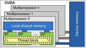 |
| Figure 23.1
NVIDIA CUDA architecture.
A GPU includes a number of multiprocessors, each consisting of several stream processors. Several threads belonging to the same thread block may execute concurrently within a multiprocessor and communicate through a small shared memory bank with fast access latency. The larger device memory has also a much higher access latency.
|
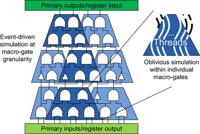
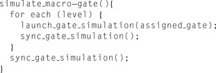
The simulation method outlined before is called “oblivious logic simulation” because all logic gates are simulated during each simulated clock cycle. However, it is often the case that, while propagating values through the netlist, for at least some gates the inputs have not changed from the previous cycle. As a result the output of those gates will also remain the same, and the computation is indeed redundant. This observation is the central idea of “event-driven simulation,” where only those gates whose input values are different from the previous simulation cycle are computed. To monitor internal value changes and determine which gates should be computed, event-driven simulation incurs a fairly large control-flow overhead. Many commercial logic simulators today are based on an event-driven scheme because the benefits from a reduced amount of gate computation well offset the cost of a centralized scheduler to manage the simulation's control flow. However, this scheduler is inherently sequential; thus, its impact is particularly negative in a massively concurrent environment such as CUDA. In our solution we wished to reap the benefits of reduced computation of the event-driven approach, while bypassing most of the associated control-flow overhead. Thus, we devised a hybrid oblivious/event-driven scheme that applies event-driven simulation at a coarse netlist granularity, that is, for large monolithic blocks of gates, and oblivious simulation within each block.
Traditional event-driven simulators rely on a centralized event queue to schedule gates that must be computed within a simulation cycle. In the context of the CUDA architecture such a queue would incur
high latency delays — most probably higher than the computation of the gates themselves. However, we noted that a dynamic scheduling approach can still be valuably exploited as long as it operates at the granularity of thread blocks, and it is thus accessed much more infrequently. As a result, we assign clusters of gates from the circuit's netlist to individual thread blocks. Each of these clusters is simulated by the assigned thread block in an oblivious fashion. At the same time, we monitor the input values of the cluster, and we use an event-driven approach in scheduling a cluster for simulation or bypassing it if none of its inputs have changed.
A high-level schematic of the approach described is presented in
Figure 23.2
, showing a pool of clusters for a netlist and a possible simulation requiring to schedule only three of the clusters for computation. Note that we call the clusters of gates “macro-gates.” To implement this design we must develop a segmentation algorithm to create macro-gates of appropriate size, striking a trade-off between performance and memory locality requirements, and additional optimizing algorithms to ensure as regular of an execution as possible within each macro-gate's oblivious simulation.
 |
| Figure 23.2
Hybrid event-driven simulator.
The novel simulator architecture is event driven at the granularity of macro-gates, while the macro-gates themselves are simulated in an oblivious fashion. The macro-gates with a darker shade are the only ones scheduled for simulation during a possible simulation cycle.
|
23.3. Compilation and Simulation
The GPU-based simulation operates in a compiled-code fashion: a compilation process is performed, mapping the netlist to internal data structures suited to the GPU memory hierarchy. Following compilation, in the simulation phase, the GPU accesses these internal data structures and updates them according to the inputs provided by the test bench. The same mapped design can be reused while running several times with many distinct test benches, allowing the compilation time to be amortized over multiple simulation runs.
Compilation consists of two phases (see
Figure 23.3
): the first phase is
system-level compilation
, where a gate-level netlist is considered as input. During this phase segmentation is applied to the netlist to partition it into a set of levelized
macro-gates
: each macro-gate includes several gates within the netlist connected by input/output relations. Companion data structures are also created for each macro-gate to facilitate event-driven simulation. The second phase is
macro-gate balancing
. During this phase each macro-gate is reshaped for efficient simulation on the GPU platform. Once compilation is completed, the data structures and the GPU kernels generated can be transferred to the GPU and simulation may begin.
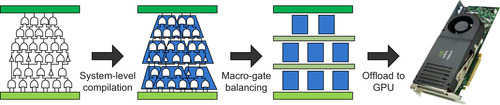 |
| Figure 23.3
Simulator organization.
The simulator performs a two-phase compilation, after which data structures and GPU kernels are transferred to the GPU, which in turn performs the simulation.
|
During the execution of the GPU program, that is, during simulation, the test bench reads the outputs generated at the end of each clock cycle and provides inputs for the next cycle. Test benches can be implemented using a variety of strategies, the most efficient of which is a direct GPU implementation, which avoids costly communication with the host CPU. Once the stimuli are exhausted, simulation comes to an end.
23.3.1. System-Level Compilation
The goal of system-level compilation is to segment the netlist into macro-gates, groups of gates that will be simulated in an oblivious fashion by a single-thread block, while different macro-gates are scheduled in an event-driven fashion. Before macro-gates can be extracted, three preprocessing steps are required:
synthesis
,
combinational logic extraction
, and
levelization
. Finally, macro-gate segmentation can be performed, producing a set of macro-gates and their associated sensitivity lists (that is, the set of inputs a macro-gate depends on).
Synthesis
The first compilation step considers a digital design and synthesizes it to a flattened netlist using a target technology library, such as the GTECH library by Synopsys in our experiments. We chose GTECH for its generality and simplicity; however, any other library may be used for this task because the simulator will replace each gate type with functional primitives; thus, a different library will simply lead to a different set of primitives. In order to enable cycle-by-cycle simulation, we used a subset of the GTECH library excluding nonclocked latches. When the netlist is read into our compiler, a functional primitive of each gate is created, internally represented by a four-valued (0, 1, X, Z) truth table. In order to maintain uniform program execution paths, all primitives use a uniform format to indicate inputs, outputs, and functionality. The primitives are frequently accessed, once for each time a gate type is simulated. To minimize the memory bandwidth required to access them, we leverage bit-level packing in storing the truth tables. As a result, the output of a gate can be determined by performing fast, efficient bit-wise operations on the packed data.
Extraction of Combinational Logic
Once the design is synthesized and mapped into internal functional primitives, the combinational portion is extracted. Because the design is simulated cycle by cycle, the contents of registers that retain state across clock cycles can be modeled as program variables. These variables store the circuit's register values: they are updated at the end of the cycle with the values computed for the register's input nets, and they are accessed for reading at the beginning of each cycle to determine the values at the register's output nets. Thus, the entire circuit can be viewed as a combinational network from the simulator's point of view. If we assume absence of combinational loops, this consists of a directed acyclic graph (DAG), a representation leveraged later during macro-gate segmentation.
Levelization
After combinational logic extraction, the combinational netlist is then
levelized
. Logic gates are organized into levels based on their topological order, so that the fan-in of all gates in one level is computed in previous levels. With this organization, it is possible to simulate the entire netlist one level at a time, from inputs to outputs, without concern for backward dependencies. In our prototype implementation, we used an ALAP (as-late-as-possible) levelization, though other solutions are also possible.
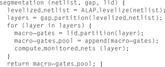
Once the design has been synthesized and the combinational logic has been extracted and levelized, macro-gate segmentation may be applied. When we view the preprocessed design as a levelized DAG, this phase partitions the graph, carving out blocks of logic referred to as macro-gates (see
Figure 23.4
). In addition to the segmentation itself, wires at the periphery of macro-gates are annotated with their relation to other macro-gates and grouped into a sensitivity list used to inform event-driven simulation.
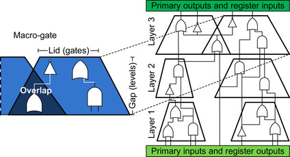 |
| Figure 23.4
Macro-gate segmentation.
The levelized netlist is partitioned into layers, each encompassing a fixed number of levels (gap). Macro-gates are then carved out by extracting the transitive fan-in from a set of nets (lid) at the output of a layer, back to the layer's input. If an overlap occurs, the gates involved are replicated for all associated macro-gates.
|
Three important factors govern the process of macro-gate segmentation: (1) because the objective of forming macro-gates is to perform event-driven simulation at a coarse granularity (compared with individual gates), the time required to simulate a given macro-gate should be substantially larger than the overhead to decide which macro-gates to activate. (2) The multiprocessors in the GPU can communicate only through high-latency device memory, and thus for best performance, there should be no communication among them. This can be ensured if the tasks executing on distinct multiprocessors are independent of each other. To this end, macro-gates that are simulated concurrently must be independent of each other. To achieve this goal, we duplicate small portions of logic that occasionally create overlap among macro-gates, eliminating the need of communication. (3) Finally, we want to avoid cyclic dependencies between macro-gates so that we can simulate each macro-gate at most once per cycle; to this end, we levelize the netlist at the granularity of macro-gates as well.
Segmentation begins by partitioning the netlist into
layers
: each layer encompasses a fixed number of the netlist's levels, as shown in
Figure 23.4
. Macro-gates are then defined by selecting a set of nets at the top boundary of a layer and including their cone of influence back to the input nets of the layer. The number of nets used to generate each macro-gate is a parameter called
lid
; its value is selected so that the number of logic gates in each macro-gate is approximately the same. The number of levels within each layer is called
gap
, and it corresponds to the height of the macro-gate. In
Section 23.3.4
we discuss how to select a suitable value for gap and lid in order to achieve a high level of parallelism during simulation, as well as maintain the event-driven structure of simulation.
While we are collecting the gates that belong to a logic cone, it is possible that gates may be assigned to two or more macro-gates. Duplication of a few gates allows macro-gates to be simulated independently, without sharing any data with other macro-gates. There can be several possible policies for selecting the output nets, whose cones of influence are clustered in a single macro-gate. In our case we aim at minimizing duplication; thus, we cluster together those nets whose cones of influence have the most gates in common. This policy is implemented in our prototype.
Figure 23.5
presents the pseudocode of the algorithm discussed in this section.
 |
| Figure 23.5
Macro-gate segmentation algorithm.
First, the netlist is levelized, and the resulting levels are grouped into layers. Each layer is then partitioned into macro-gates, which are then added to the pool to be simulated. The nets to be monitored for switching activity (which indicate the need for a macro-gate to be scheduled for simulation) are also collected at this stage.
|
23.3.2. Macro-Gate Balancing
After macro-gate segmentation, each macro-gate is treated as an independent block of logic gates to be simulated by concurrent threads. The threads operating on an individual macro-gate must belong to the same thread block for resource sharing, and thus, they execute in the same multiprocessor of a GPU. The macro-gate balancing step, presented in this section, reshapes each macro-gate to enable the best use of execution resources.
To maximize resource usage, all threads should be busy for the entire execution of a macro-block simulation. This efficiency goal is challenged by the typical shape of macro-gates: a large base (many gates) close to the primary inputs and a narrower tip (very few gates toward the outputs), resulting in a trapezoidal shape. This shape is the by-product of the macro-gate generation process, that is, the selection of a few output wires and their fan-in logic cones, as discussed in macro-gate segmentation in
Section 23.3.1
. Thus, a large number of active threads are required at the lower levels and just a few in the levels close to the top, where just a few gates must be simulated. The process of macro-gate balancing is illustrated qualitatively in
Figure 23.6
: balancing moves gates toward the upper levels of the netlist, within the slack allowed by their input/output connections. The result after balancing is a macro-gate where the number of gates at each level is equalized as much as possible. Note also that balancing may increase the overall gap of the macro-gate.
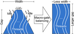 |
| Figure 23.6
Macro-gate balancing.
The balancing algorithm restructures each macro-gate to minimize the number of concurrent execution threads required. The result is a more efficient utilization of thread-block resources.
|
The macro-gate balancing algorithm outlined in
Figure 23.7
exploits the slack available in the levelized netlist within each macro-gate and reshapes it to have approximately the same number of logic gates in each level. The algorithm processes all the gates in a bottom-up fashion, filling every slot in the macro-gate with logic gates, with the goal of assigning each gate to the lowest level possible, while
maintaining the restriction on maximum width. Note that this might also lead to an increase in the height of a particular macro-gate and thus its simulation latency. Hence, there is an inherent trade-off between execution latency and thread utilization.
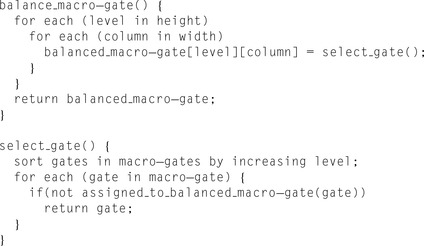 |
| Figure 23.7
Macro-gate balancing algorithm.
Macro-gates are considered one at a time and reshaped to fit into a thread block with a preset maximum number of threads, while trying to minimize the number of logic levels. The algorithm proceeds in a bottom-up fashion, filling each level of the macro-gate with logic gates.
|
23.3.3. Simulation Phase
Simulation is carried out directly on the GPU coprocessor, evaluating the gates within each macro-gate in an oblivious fashion and using event-driven scheduling for macro-gates. Event-driven scheduling is informed by sensitivity lists, used to determine which macro-gates to activate in the subsequent layer. During simulation, concurrency is exploited at two different levels of abstraction: several macro-gates can be simulated in parallel using distinct thread blocks (and multiprocessors); in addition, within each macro-gate, gates at the same level can be computed concurrently by different individual threads.
Each macro-gate is assigned to a distinct thread-block; thread blocks are then grouped and scheduled to distinct multiprocessors by the CUDA scheduler. Macro-gates are scheduled layer by layer, simulating all the activated macro-blocks in one layer before proceeding to the next, as shown in
Figure 23.8
. The sensitivity list of each macro-gate (that is, its monitored nets) informs the event-driven simulation scheduler, which determines which macro-gates in a layer require simulation.
 |
| Figure 23.8
Event-driven simulation
proceeds layer by layer at the macro-gate granularity. Within each layer, activated macro-gates are simulated, and monitored nets are analyzed to activate a subset of the next layer's macro-gates. Activated macro-gates are transferred by the CUDA scheduler to an available multiprocessor for simulation.
|
Simulation is driven by two kernels (GPU programs) alternating their execution on the GPU. First, the
simulation kernel
simulates all active macro-gates in a layer. Execution of the
scheduling kernel
follows, evaluating the array of monitored nets to determine which macro-gates should be activated in the next layer. This array is organized as a bit vector, with each monitored net being implicitly mapped to a unique location in the array. If a macro-gate simulation from a previous layer modifies the value of any of these nets, its corresponding array index is tagged. Each macro-gate has a corresponding
sensitivity list
where all the input nets triggering its activation are tagged. With this structure, a simple bit-wise AND operation between the monitored net's array and a macro-gate's sensitivity list determines if any input change has occurred and whether the macro-gate should be activated. A schematic overview of this process is illustrated in
Figure 23.8
; in addition,
Figure 23.9
provides a simple pseudocode of the flow just presented.
 |
| Figure 23.9
Event-driven simulation scheduler.
The scheduling algorithm considers all macro-gates in the next layer of simulation and intersects their sensitivity list with the monitored nets that have switched during the current simulation cycle. Each macro-gate that finds a nonzero intersection is then scheduled for simulation in the next layer.
|
Data placement for simulation is organized so that primary inputs, outputs, register values, and monitored nets are mapped to device memory because they must be shared among several macro-gates (multiprocessors). The netlist structure is also stored in device memory and accessed during each macro-gate simulation.
Oblivious Simulation within Macro-Gates
Individual macro-gates are simulated by a thread block; each thread within the block is responsible for computing the output of one distinct logic gate. All threads in the thread block synchronize after
the simulation of each netlist level of the macro-gate is completed so that all the output values from previous levels are updated before the next level's gates are computed.
Figure 23.10
illustrates this process by showing which gate output values are computed by each thread during the simulation. Note that in the right part of the figure, distinct threads are spread horizontally, while time progresses vertically. The shared memory associated with each multiprocessor is used to store the truth tables for all gates in the technology library and internal net values for the macro-gate. Truth tables are stored in shared memory because of their frequent access during simulation. Intermediate nets values (internal
gates outputs) are also potentially accessed by several gates (and, thus, threads) during a macro-gate simulation. However, macro-gate topologies are stored in device memory, and each thread fetches its corresponding gate information from there. In device memory, logic gates are stored in a regular matrix-like fashion and the location of each gate corresponds to the position of the output nets of the logic gates of a balanced macro-gate.
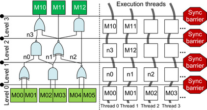 |
| Figure 23.10
Oblivious simulation within a macro-gate.
The logic gates within a macro-gate are simulated in an oblivious fashion. Each thread is responsible for computing the output of one gate at a time: vertical waved lines connect the set of logic gates for which a single thread is responsible at subsequent time intervals. Note that each level is kept synchronized within the block by a synchronization barrier.
|
They also correspond to the layout of the nets in shared memory, thus creating the scope of very regular execution suited for GPU. Each thread simulating a gate gathers the relevant information from device memory, that is, location of input nets and type of logic function. Note, however, that balanced macro-gates have a fairly regular structure; thus all this information can be coalesced to limit the number of device memory accesses. Input net values are then retrieved from shared memory and a truth table access determines the output value of this gate, which is subsequently written to shared memory. Upon completion of a macro-gate simulation, output values are transferred to device memory to determine if a value change has occurred since the previous simulation cycle. The oblivious simulation kernel (one thread's designated work) is presented in the pseudocode of
Figure 23.11
. Concurrent execution of this kernel by all threads within a thread block results in the simulation of a complete macro-gate.
 |
| Figure 23.11
Oblivious simulation routine for an individual thread.
The routine is executed by each thread within a thread block. Each thread operates on a different set of gates, and a complete macro-gate is simulated after the last synchronization step.
|
Test Benches
Test benches are an important part of simulation because simulation is only useful when the design is validated with a relevant sequence of stimuli. Hence, we need to provide methods of incorporating test benches. Because the simulator is cycle based, the task of the test bench is to read the outputs computed at the end of every cycle and provide suitable inputs for the next cycle. In our solution, test benches are implemented as separate GPU kernels: during simulation, the kernels for simulation proper and those for the test bench alternate execution on the GP-GPU device. At the completion of each simulation cycle, the outputs produced by the netlist are read from device memory, and suitable inputs are computed and written there to be consumed during the following simulation cycle. We developed several ways of implementing the test bench kernels, each appropriate for different types of designs and simulation setups. The two fundamental types of test-bench kernels are synthesizable ones and software kernels emulating a behavioral hardware description.
Synthesizable Test Benches
These test benches can be expressed by synthesizable hardware descriptions. As a result they can be synthesized and represented by a netlist, similarly to the design under simulation. In these situations the alternating of test-bench and simulation kernels can be viewed as a cosimulation: the two kernels are
identical; they simply operate on different netlists. The result is very high-performance kernels, which can completely reside on the GPU device.
Software Test Benches
In other situations, test benches can be described as GPU's software programs reading input values from device memory at each clock cycle and producing outputs for the next simulation step. A classic example of this type of test bench is a microprocessor test kernel, a simple kernel that is often used when simulating a microprocessor design executing a binary program. The test bench is responsible for providing instructions from the binary program to the microprocessor design as well as processing its load/store data memory accesses. The program is stored in device memory: at each simulation cycle the test bench also serves memory requests by the microprocessor.
Other Test Benches
Other complex test benches involving constructs that cannot be expressed in a CUDA kernel can still be executed on the host CPU, but an additional communication penalty is incurred with every simulation cycle.
23.3.4. Macro-Gate Sizing Heuristics
The key to simulation performance lies in the quality of macro-gate partitioning. Event-driven simulation is most efficient when only a small fraction of macro-gates are active in each given cycle. Consequently, the selection of which gates to include in each macro-gate is a critical aspect of our simulator architecture, as discussed in macro-gate segmentation in
Section 23.3.1
.
The size of a macro-gate is governed by two parameters, gap and lid, which control the granularity of the event-driven mechanism. The goal in selecting the values for these parameters is to create macro-gates with low-activation rates. Gap and lid values are selected during the compilation phase by evaluating a range of candidate <gap,lid> value pairs; for each candidate pair, we collect several metrics: number of macro-gates generated, number of monitored nets, size of macro-gates, and their activation rate. The activation rate is obtained by a simulation mock-up on a micro test bench. We then select optimal values among those considered and perform detailed segmentation.
Figure 23.12
shows an example of this selection process for one of our experimental evaluation designs, reporting simulation times. In this example, the best performance is achieved at <gap,lid> = <5,100>.
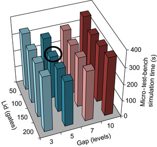 |
| Figure 23.12
Optimal gap and lid estimation
for a low-density parity check (LDPC) encoder design. The figure plots the execution time of a micro test-bench simulation with a range of gap and lid values. The dark circle highlights the optimal selection of values among those considered.
|
Boundaries for the range of gap values considered are derived from the number of monitored nets generated: we consider gap values only for which no more than 50% of the total nets are monitored. In practice, small gap values tend to generate many monitored nets, while large gap values trigger high-activation rates. In selecting the range of lid values to consider, we bound the analysis by estimating how many macro-gates will be created at each layer, striving to run all the macro-gates concurrently in the GPU, even in the worst case. The GPU used for our evaluation (8800GT) included 14 multiprocessors, and the CUDA scheduler allowed for at most three thread blocks executing concurrently on the same multiprocessor. Thus, we considered only lid values that generate no more than 14 × 3 = 42 macro-gates per layer. Note that this analysis is performed only once per compilation.
23.4. Experimental Results
We evaluated the performance of our simulator on a broad set of designs, ranging from purely combinational circuits, such as a low-density parity check (LDPC) encoder, to a multicore SPARC design
containing over 1 million logic gates. Designs were obtained from the OpenCores suite
[12]
and from the Sun OpenSPARC project
[15]
; we also considered two Alpha ISA-based microprocessors and two network-on-chip (NoC) systems developed in advanced digital design courses by student teams at the University of Michigan.
We report in
Table 23.1
the key aspects of these designs: number of gates, flip-flops and type of stimulus that was used during simulation. The complexity of the test benches is expressed in terms of lines of code in the original verilog test bench (see the column named No. LOC). The first two designs are processors implementing the Alpha instruction set; the first can execute one instruction at a time, whereas the second is a five-stage pipelined architecture. Both were simulated executing a binary program that computed Fibonacci series recursively. The LDPC encoder outputs an encoded version of its input; for this design, we developed a random stimulus generator that runs directly on the GPU platform. The JPEG decompressor decodes an image provided as input. The NoC designs consist of a network of five-channel routers connected in a torus topology and simulated with a random stimulus generator transmitting packets across the network. Finally, the OpenSPARC designs are composed of processor cores from the OpenSPARC T1 multicore chip (excluding caches) and run a conglomeration of assembly regressions provided with Sun's open source distribution. We built several versions of this processor: single core, two cores, and four cores; and we emulated local cache activity by leveraging playback of prerecorded signal traces from processor-crossbar and processor-cache interactions.
23.4.1. Macro-Gates
Macro-gate segmentation partitions the design into clusters to be simulated in an event-driven fashion, while gates within each macro-gate are simulated in an oblivious fashion. Thus, the effectiveness of the
macro-gate segmentation process has a strong impact on performance. We studied several aspects of the compilation phase of our simulator, including the number of macro-gates resulting from segmentation and their size. Additionally, we explored the extent of gate replication among macro-gates.
Table 23.2
presents the characteristics of the macro-gates that result from segmentation of each design. We report the gap and lid values used to segment the designs, as determined by the process described in
Section 23.3.4
. Additionally, the fourth column indicates the number of layers obtained by segmenting with the reported gap. The total number of macro-gates that were formed as a result of segmentation for each design is also reported, as well as their average, maximum, and minimum size in terms of logic gates. Note that the largest design, OpenSPARC-4 cores, includes many more
macro-gates in each layer that could be simulated concurrently (42 as computed in
Section 23.3.4
) because it has 2955 macro-gates distributed over only 28 layers.
As mentioned in macro-gate segmentation in
Section 23.3.1
, gate replication is a necessary consequence of the high communication latency between multiprocessors. However, we strive to keep replication low, so as not to inflate the number of simulated gates during each cycle.
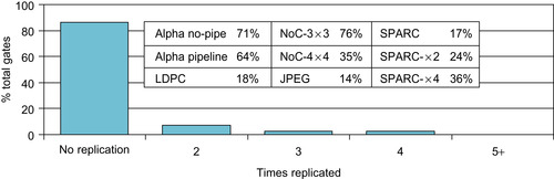
Figure 23.13
plots the fraction of gates that incurred replication, averaged over all our experimental designs: more than 80% incurred no replication, less than 10% were simply duplicated, and very few incurred a higher degree of replication. The table inset reports the rate of “gate inflation” for each design, resulting in an overall average of 39%.
 |
| Figure 23.13
Gate replication resulting from macro-gate overlap.
The graph reports the number of times that gates have been replicated in order to obtain independent macro-gates. The inset table indicates the gate inflation that each design incurred as a result of this process.
|
23.4.2. Monitored Nets
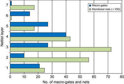
The number of monitored nets has a high impact on simulator performance; thus, segmentation strives to keep the fraction of nets that are monitored low. As an example, in
Figure 23.14
, we plot the structure of the LDPC encoder design after segmentation: for each layer, we plot the corresponding number of macro-gates and monitored nets. Note how middle layers tend to have more macro-gates than peripheral layers and how lower layers tend to generate the most monitored nets. Finally, we analyzed the fraction of total nets in the design that requires monitoring because they cross layer boundaries. The compilation phase should strive to keep this fraction low because it directly relates to the size of the sensitivity list.
Figure 23.15
reports our findings for the designs in our evaluation pool.
 |
| Figure 23.14
Segmented structure for LDPC encoder design.
The plot shows the geometry of the LDPC encoder after segmentation. For each layer we report the number of macro-gates and of monitored nets in hundreds.
|
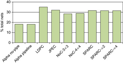 |
| Figure 23.15
Fraction of monitored nets.
Percentage of all nets that must be monitored for each design in our experimental evaluation.
|
23.4.3. Design Compilation
As part of our experimental evaluation, we consider the time spent in compiling the design for simulation on the GPU-based simulator.
Table 23.3
reports separate times for the system-level compilation phase and for the balancing phase in compiling each design. The table also indicates the total compilation time and compares that data against that of a commercial logic simulator executing on a general processor machine. The commercial simulator that we used for the comparison is considered among the fastest available in the market today. Note that the compilation time is not a critical aspect in the
performance of a simulator because this time can be amortized over many simulations and over very long (hours or days) simulation runs. However, we felt it was relevant to convey information on the timescale of compilation performance.
23.4.4. Macro-Gate Activity
The activation rate of macro-gates is an important metric for event-driven simulation; by comparison, an oblivious simulator has an activation rate of 100% on any design. The goal of an event-driven
simulator is to keep this rate as low as possible, thus leveraging the fact that not all gates in a netlist switch on every cycle.
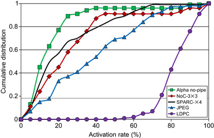
Figure 23.16
reports the macro-gate activation rates for a number of the evaluation designs. Individual plots show the cumulative distribution of activation rates among all the macro-gates for a given design. Note that, for most designs, most macro-gates have an activation rate
of only 10 to 30%. However, for LDPC, most macro-gates experience a high-activation rate (> 80%): this is due to the inherent nature of the design, which requires evaluation of all the bits positions for each parity check. The designs that are not reported have a cumulative distribution similar to that of the OpenSPARC and NoC designs. Note that the activation rate for our solution does not directly relate to performance gain over oblivious simulation. As an example, the JPEG decoder has an average activation rate of 40%. This does not mean that, on average, the JPEG decoder is simulated 2.5 times faster when compared against an oblivious simulation. Indeed, even if very few macro-gates are activated, one for each layer, the performance would be just the same as if several macro-gates were simulated in each layer. This is because of the parallelism of the underlying hardware, capable of simulating many macro-gates in a same layer simultaneously, coupled with synchronization barriers that force macro-gates to be simulated in layer order. In the end, the overall performance of the JPEG design in event-driven simulation is 1.55 times faster than in oblivious simulation.
 |
| Figure 23.16
Macro-gates activation.
Cumulative distribution of macro-gates with respect to the activation rate. The plots show the fraction of macro-gates with an activation rate below the threshold indicated on the horizontal axis. For most designs, a majority of the macro-gates have an activation rate below 30%, indicating that the segmentation parameters selected are effective in reducing the amount of computation in event-driven simulation.
|
23.4.5. Performance Evaluation
Finally, we evaluated the performance of our prototype event-driven simulator against that of a commercial, event-driven simulator for a general-purpose processor system. The commercial simulator we selected is known to be among the fastest (or the fastest) available in the market today. Our graphics coprocessor was a CUDA-enabled 8800GT GPU with 14 multiprocessors and 512MB of device memory, operating at 600MHz for the cores and at 900MHz for the memory. Device memory size was not a limitation in any of our experiments, as all data structures, including stimuli data, occupied always less than 200MB. However, it is possible that, for even larger designs, device memory becomes a storage bottleneck. The commercial simulator executed on a 2.4GHz Intel Core 2 Quad running Red Hat Enterprise Linux 5, using four parallel simulation threads.
Table 23.4
shows the performance evaluation results: for each design we report the number of cycles simulated, the runtimes in seconds for both the GPU-based simulator and the commercial simulator (compilation times are excluded), and the
relative speedup. Note that our prototype simulator outperforms the commercial simulator by 4 to 44 times, depending on the design. Note that, despite the LDPC encoder having a very high-activation rate, we report the best performance improvement for this design. As mentioned earlier, most gates in this design are switching every cycle: while this affects our activation rates, it also hampers the sequential simulator performance. Thus, the improvement obtained for this design is due to sheer parallelism of our simulator architecture.
23.5. Future Directions
Through our experience in the design and evaluation of the hybrid event-driven logic simulator, we noted that the formation of macro-gates has a strong impact on the performance of the simulator. In particular, macro-gates containing even a single frequently activated logic gate will trigger frequent simulation of the entire macro-gate, degrading overall system performance. As an alternative strategy, we plan to consolidate these logic cones with frequently activated logic gates into the same macro-gate, basically clustering based on activity instead of logic sharing.
Our baseline clustering algorithm, which considers only the degree of logic sharing, results in many macro-gates with a high-activation frequency. In
Figure 23.17(a)
we illustrate this problem qualitatively, by shading in dark gray logic cones that are activated more frequently. The proposed algorithm is illustrated in
Figure 23.17(b)
, where clustering is based on switching activity profiles, thus resulting in some highly activated macro-gates and other rarely activated ones. Activity-based clustering creates a higher separation between the activation frequency of distinct macro-gates, leading to overall improved performance.
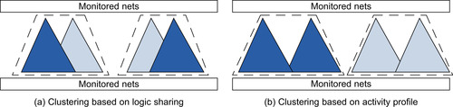 |
| Figure 23.17
Activity-based clustering
compared against the baseline solution. (a) Our baseline solution clusters logic gates by degree of sharing, while (b) activity-based clustering is based on the activation frequency of logic cones. The darkness of a cone in the picture is qualitatively proportional to its activation frequency. Clustering based on activity profile results in the consolidation of frequently activated logic cones.
|
The potential downside of this approach is in the higher gate duplication that would result from activity-based clustering. However, we expect that this cost will be negligible when compared with the significant reduction in the total number of macro-gates (and gates) dynamic simulations. This can be seen as a trade-off, shown in the figure by the lesser overlap of the cones. This trade-off is amortized by the significant reduction in the total number of macro-gate simulations that must be performed. We
plan to use profiling to estimate activity profiles, first simulating a micro test bench on a segmented circuit using the baseline clustering policy based on logic sharing. Once activity estimates of individual cones are computed, the segmentation process will be applied again, but this time cones will be added to macro-gates based on activation frequency. Future plans include a detailed study of the performance gain that can be obtained by this enhanced clustering method.
We also intend to explore the possible advantages of a more flexible segmentation scheme where the value of gap and lid are not constant throughout the entire netlist. Indeed, by allowing varying gap and lid values, we should be able to generate macro-gates with a narrower size range, leading to an even better thread utilization during simulation.
Related Work
For several decades the majority of the validation effort in industry has revolved around logic simulators. Initial works from the 1980s addressed several key algorithmic aspects that are still utilized in modern commercial solutions, including netlist compilation, scheduling solutions for event-driven simulators, propagation delays, and so on
[2]
and
[10]
. The exploration of parallel algorithms for simulation started at approximately the same time: Baker
et al
.
[1]
provide a comparative analysis of early attempts to parallelize event-driven simulation by partitioning the processing of individual events across multiple machines with fine granularity. Both shared memory multiprocessors
[9]
and distributed memory systems
[11]
have been targeted as the underlying parallel execution resource.
Only recently the effort of parallelizing simulation algorithms has started to target data-streaming architectures (single-instruction, multiple-data), as in the solution proposed by Perinkulam,
et al
.
[13]
. However, the communication overhead of that system had a high impact on overall performance, leading to no overall benefit. Another recent solution in this space introduced parallel fault simulation on a CUDA GPU target
[7]
, which derives its parallelism by simulating distinct fault patterns on distinct processing units, with no partitioning within individual simulations, nor in the design. In contrast, we target fast simulation of complex designs, which requires specialized algorithms to partition the netlist and leverages solutions to stress memory locality in order not to lose the performance advantage on memory access latency. We have performed preliminary studies in this direction using oblivious
[4]
and event-driven
[3]
simulation architectures. Moreover, we focus on optimizing the performance of individual simulation runs, in contrast with
[7]
, which optimizes over all faults simulations.
Recently, acceleration of many diverse computation-intensive processes using general-purpose graphics processing units (GP-GPU) has been explored, in several domains of EDA, such as power grid analysis
[14]
, statistical timing analysis
[8]
and fault table generation
[6]
. Utilizing GP-GPUs to accelerate few core algorithms that are shared across many EDA applications has also been proposed in
[5]
.
References
[1]
W. Baker, A. Mahmood, B. Carlson,
Parallel event-driven logic simulation algorithms: tutorial and comparative evaluation
,
IEEE J. Circuits Devices Syst.
143
(4
) (1996
)
177
–
185
.
[2]
Z. Barzilai, J. Carter, B. Rosen, J. Rutledge,
HSS–a high-speed simulator
,
IEEE Trans. Comput. Aided. Des.
6
(4
) (1987
)
601
–
617
.
[3]
D. Chatterjee, A. DeOrio, V. Bertacco,
Event-driven gate-level simulation with GP-GPUs
,
In:
Proceedings of the 46th Annual Design Automation Conference, 26–31 July 2009, San Francisco, California, DAC’09
(2009
)
ACM
,
New York
, pp.
557
–
562
.
[4]
D. Chatterjee, A. DeOrio, V. Bertacco,
GCS: high-performance gate-level simulation with GP-GPUs
,
In:
Proceedings of the Design, Automation & Test in Europe Conference & Exhibition, 20–24 April 2009, Nice, France, DATE’09
(2009
)
IEEE Computer Society
,
Washington, DC
, pp.
1332
–
1337
.
[5]
Y.S. Deng, B.D. Wang, S. Mu,
Taming irregular EDA applications on GPUs
,
In:
Proceedings of the 2009 International Conference on Computer-Aided Design, 02–05 November 2009, San Jose, California, ICCAD’09
(2009
)
ACM
,
New York
, pp.
539
–
546
.
[6]
K. Gulati, S. Khatri,
Fault table generation using graphics processing units
,
In:
Proceedings High Level Design Validation and Test Workshop, 2009. 4–6 November 2009, San Francisco, California, HLDVT
(2009
)
IEEE Computer Society
,
Washington, DC
, pp.
60
–
67
.
[7]
K. Gulati, S.P. Khatri,
Towards acceleration of fault simulation using graphics processing units
,
In:
Proceedings of the 45th Annual Design Automation Conference, 08–13 June 2008, Anaheim, California, DAC’08
(2008
)
ACM
,
New York
, pp.
822
–
827
.
[8]
K. Gulati, S.P. Khatri,
Accelerating statistical static timing analysis using graphics processing units
,
In:
Proceedings of the 2009 Asia and South Pacific Design Automation Conference, 19–22 January 2009, Yokohama, Japan
(2009
)
IEEE Press
,
Piscataway, NJ
, pp.
260
–
265
.
[9]
H.K. Kim, S.M. Chung,
Parallel logic simulation using time warp on shared-memory multiprocessors
,
In:
Proceedings of the 8th International Symposium on Parallel Processing, April 1994, Cancún, Mexico
(1994
)
IEEE Computer Society
,
Washington, DC
, pp.
942
–
948
.
[10]
D. Lewis,
A hierarchical compiled code event-driven logic simulator
,
IEEE Trans. Comput. Aided. Des.
10
(6
) (1991
)
726
–
737
.
[11]
Y. Matsumoto, K. Taki,
Parallel logic simulation on a distributed memory machine
,
In:
Proceedings of the 3rd European Conference on Design Automation, 16–19 March 1992 Brussels, Belgium, EDAC’92
(1992
)
IEEE Computer Society
,
Washington, DC
, pp.
76
–
80
.
[12]
Opencores,
http://www.opencores.org/
.
[13]
A. Perinkulam, S. Kundu, Logic simulation using graphics processors, in: Proceedings 14th International Test Synthesis Workshop, 5–7 March 2007, San Antonio, Texas, ITSW’07.
[14]
J. Shi, Y. Cai, W. Hou, L. Ma, S.X.-D. Tan, P.-H. Ho,
et al.
,
GPU friendly fast Poisson solver for structured power grid network analysis
,
In:
Proceedings of the 46th Annual Design Automation Conference, 26–31 July 2009, San Francisco, California, DAC’09
(2009
)
ACM
,
New York
, pp.
178
–
183
.
[15]
Sun microsystems OpenSPARC,
http://opensparc.net/
.
..................Content has been hidden....................
You can't read the all page of ebook, please click here login for view all page.