
Chapter 24. GPU-Based Parallel Computing for Fast Circuit Optimization
Yifang Liu and Jiang Hu
The progress of GPU (graphics processing unit) technology opens a new avenue for boosting computing power. This chapter exploits the GPU to accelerate VLSI circuit optimization. We present GPU-based parallel computing techniques and apply them on solving simultaneous gate sizing and threshold voltage assignment problem, which is often employed in practice for performance and power optimization. These techniques are aimed at utilizing the benefits of GPU through efficient task scheduling and memory organization. Compared against conventional sequential computation, our techniques can provide up to 56× speedup without any sacrifice on solution quality.
Fast circuit optimization technique is used during chip design. Although the pressure of time-to-market is almost never relieved, design complexity keeps growing along with transistor count. In addition, more and more issues need to be considered — from conventional objectives like performance and power to new concerns like process variability and transistor aging. On the other hand, the advancement of chip technology opens new avenues for boosting computing power. One example is the amazing progress of GPU technology. In the past five years, the computing performance of GPU has grown from about the same as a CPU to about 10 times that of a CPU in term of GFLOPS
[4]
. GPU is particularly good at coarse-grained parallelism and data-intensive computations. Recently, GPU-based parallel computation has been successfully applied for the speedup of fault simulation
[3]
and power-grid simulation
[2]
.
In this work, we propose GPU-based parallel computing techniques for simultaneous gate sizing and threshold voltage assignment. Gate sizing is a classic approach for optimizing performance and power of combinational circuits. Different size implementations of a gate realize the same gate logic, but present a trade-off between the gate's input capacitance and output resistance, thus affecting the signal propagation delay on the gate's fan-in and fan-out paths, as well as the balance between timing performance and power dissipation of the circuit. Threshold voltage (V
t
) assignment is a popular technique for reducing leakage power while meeting a timing performance requirement. It is a trade-off factor between the signal propagation delay and power consumption at a gate. Because both of these two circuit optimization methods essentially imply a certain implementation for a logic gate, it
is not difficult to perform them simultaneously. It is conceivable that a simultaneous approach is often superior to a separated one in terms of solution quality.
To demonstrate the GPU-based parallelization techniques, we use as an example of the simultaneous gate sizing and
V
t
assignment problem, which minimizes the power dissipation of a combinational circuit under timing (performance) constraint. The problem is formulated as follows.
Timing-Constrained Power Optimization:
Given the netlist of a combinational logic circuit
G
(V
,
E
), arrival times (AT) at its primary inputs, required arrival times (RAT) at its primary outputs, and a cell library, in which each gate
v
i
has a size implementation set
W
i
and a
V
t
implementation set
U
i
, select an implementation (a specific size and
V
t
level) for each gate to minimize the power dissipation under timing constraints, that is,
 where
w
i
and
u
i
are the size and the
V
t
level of gate
v
i
, respectively,
D
(v
j
, v
i
) is the signal propagation delay from gate
v
j
to gate
v
i
,
p
i
is the power consumption at gate
v
i
, and
I
(G
) is the primary inputs of the circuit.
where
w
i
and
u
i
are the size and the
V
t
level of gate
v
i
, respectively,
D
(v
j
, v
i
) is the signal propagation delay from gate
v
j
to gate
v
i
,
p
i
is the power consumption at gate
v
i
, and
I
(G
) is the primary inputs of the circuit.
For the optimization solution, we focus on discrete algorithm because (1) it can be directly applied with cell library-based timing and power models, and (2)
V
t
assignment is a highly discrete problem. Discrete gate sizing and
V
t
assignment faces two interdependent difficulties. First, the underlying topology of a combinational circuit is typically a DAG (directed acyclic graph). The path reconvergence of a DAG makes it difficult to carry out a systematic solution search like dynamic programming (DP). Second, the size of a combinational circuit can be very large, sometimes with dozens of thousands of gates. As a result, most of the existing methods are simple heuristics
[1]
. Recently, a Joint Relaxation and Restriction (JRR) algorithm
[5]
was proposed to handle the path reconvergence problem and enable a DP-like systematic solution search. Indeed, the systematic search
[5]
remarkably outperforms its previous work. To address the large problem size, a grid-based parallel gate sizing method was introduced in
[10]
. Although it can obtain high-solution quality with very fast speed, it concurrently uses 20 computers and entails significant network bandwidth. In contrast, GPU-based parallelism is much more cost-effective. The expense of a GPU card is only a few hundreds of dollars, and the local parallelism obviously causes no overhead on network traffic.
It is not straightforward to map a conventional sequential algorithm onto GPU computation and achieve desired speedup. In general, parallel computation implies that a large computation task needs to be partitioned to many threads. For the partitioning, one needs to decide its granularity levels, balance the computation load, and minimize the interactions among different threads. Managing data and memory is also important. One needs to properly allocate the data storage to various parts of the memory system of a GPU. Apart from general parallel computing issues, the characteristics of the GPU should be taken into account. For example, the parallelization should be SIMD (single instruction multiple data) in order to better exploit the advantages of GPU. In this work, we propose task-scheduling
techniques for performing gate-sizing/
V
t
assignment on the GPU. To the best of our knowledge, this is the first work on GPU-based combinational circuit optimization. In the experiment, we compare our parallel version of the joint relaxation and restriction algorithm
[5]
with its original sequential implementation. The results show that our parallelization achieves speedup of up to 56× and 39× on average. At the same time, our techniques can retain the exact same solution quality as
[5]
. Such speedup will allow many systematic optimization approaches, which were slow and previously regarded as impractical, to be widely adopted in realistic applications.
24.2. Core Method
24.2.1. Algorithm for Simultaneous Gate Sizing and
V
t
Assignment
We briefly review the simultaneous gate sizing and
V
t
assignment algorithm proposed in
[5]
, because the parallel techniques proposed here are built upon this algorithm. This algorithm has two phases: relaxation phase and restriction phase. It is called Joint Relaxation and Restriction (JRR). Each phase consists of two or more circuit traversals. Each traversal is a solution search in the same spirit as dynamic programming. The main structure of the algorithm is outlined in
Algorithm 1
. For the ease of description, we call a combination of certain size and
V
t
level as an implementation of a gate (or a node in the circuit graph).
The relaxation phase includes two circuit traversals: history consistency relaxation and history consistency restoration. The history consistency relaxation is a topological order traversal of the given circuit, from its primary inputs to its primary outputs. In the traversal, a set of partial solutions is propagated. Each solution is characterized by its arrival time (a
) and resistance (r
). A solution is pruned without further propagation if it is inferior on both
a
and
r
. This is very similar to the dynamic programming-based buffer insertion algorithm
[10]
. However, the topology here is a DAG as opposed to a tree in buffer insertion. Therefore, two fan-in edges
e
1
and
e
2
of a node
v
i
may have a common ancestor node
v
j
. When solutions from
e
1
and
e
2
are merged, normally one needs to ensure that they are based on the same implementation at
v
j
. This is called history consistency constraint. When a DP-like algorithm is applied directly on a DAG, this constraint requires all history information to be kept or traced, and consequently causes substantial computation and memory overhead. To overcome this difficulty, Liu and Hu
[5]
suggest to relax this constraint in the initial traversal; that is, solutions are allowed to be merged even if they are based on different implementations of their common ancestor
nodes. Although the resulting solutions are not legitimate, they provide a lower bound to the
a
at each node, which is useful for subsequent solution search.
In the second traversal of the relaxation phase, any history inconsistency resulted from the first iteration is resolved in a reverse topological order, from the primary outputs to the primary inputs. When a node is visited in the traversal, only one implementation is selected for the node. Hence, no history inconsistency should exist after the traversal is completed. The implementation selection at each node is to maximize the timing slack at the node. The slack can be easily calculated by the required arrival time (q
), which is propagated along with the traversal, and the
a
obtained in the previous traversal.
The solution at the end of the relaxation phase can be further improved. This is because the solution is based on the
a
obtained in the relaxation, which is not necessarily an accurate one. Because of the relaxation, the
a
is just a lower bound, which implies optimistic deviations. Such deviations are compensated in the restriction phase. In contrast to relaxation, where certain constraints are dropped, restriction imposes additional constraints to a problem. Both relaxation and restriction are for the purpose of making the solution search easy. A restricted search provides a pessimistic bound to the optimal solution. Using pessimistic bounds in the second phase can conceivably compensate the optimistic deviation of the relaxation phase.
The restriction phase consists of multiple circuit traversals with one reverse topological order traversal following each topological order traversal. Each topological order traversal generates a set of candidate solutions at each node, with certain restrictions. Each reverse topological order traversal selects only one solution in the same way as the history consistency restoration traversal in the relaxation phase. A topological order traversal starts with an initial solution inherited from the previous traversal. The candidate solution generation is also similar to the DP-based buffer insertion algorithm. The restriction is that only those candidate solutions based on the initial solution are propagated at every multifan-out node. For example, at a multifan-out node
v
i
, candidate solutions are generated according to their implementations, but only the candidates that are based on the initial solution of
v
i
are propagated toward their child nodes. By doing so, the history consistency can be maintained throughout the traversal. The candidate solutions that are not based on the initial solution are useful for the subsequent reverse topological order traversal.
The description so far is for the problem of maximizing timing slack. For problem formulations where timing performance, power consumption, and/or other objectives are considered simultaneously, one can apply the Lagrangian relaxation technique together with the algorithm of Joint Relaxation and Restriction
[5]
.
24.2.2. GPU-Based Parallelization
A GPU is usually composed of an array of multiprocessors, and each multiprocessor consists of multiple processing units (or ALUs). Each ALU is associated with a set of local registers, and all the ALUs of a multiprocessor share a control unit and some shared memory. There is normally no synchronization mechanism between different multiprocessors. A typical GPU may have over 100 ALUs. GPU is designed for SIMD parallelism. Therefore, an ideal usage of GPU is to execute identical instructions on a large volume of data, each element of which is processed by one thread.
The software program applied on GPU is called kernel function, which is executed on multiple ALUs in the basic unit of thread. The threads are organized in a two-level hierarchy. Multiple threads form a warp, and a set of warps constitutes a block. All warps of the same block run on the same
multiprocessor. This organization is for convenience of sharing memory and synchronization among thread executions. The thread blocks are often organized in a three-dimensional grid, just as threads in themselves are. The global memory for a GPU is usually a DRAM off the GPU chip, but on the same board as GPU. The latency of global memory access can be very high, owing to the small cache size. Similarly, loading the kernel function onto the GPU also takes a long time. In order to improve the efficiency of GPU usage, one needs to load data infrequently and make the ALUs dominate the overall program runtime.
Two-Level Task Scheduling
: Our GPU-based parallelism for gate sizing and
V
t
assignment is motivated by the observation that the algorithm repeats a few identical computations on many different gates. When evaluating the effect of an implementation (a specific gate and
V
t
level) for a gate, we compute its corresponding AT, RAT, and power dissipation. These few computations are repeated for many gates, sometimes hundreds of thousands of gates, and for multiple iterations
[5]
. Evidently, such repetitive computations on a large number of objects fit very well with SIMD parallelism.
We propose a two-level task-scheduling method that allocates the computations to multiple threads. At the first level, the computations for each gate are allocated to a set of thread blocks. The algorithm, software, and hardware units of this level are gate, thread block, and multiprocessor, respectively. Because different implementations of a gate share the same context (fan-in and fan-out characteristics), such allocation matches the shared context information with the shared memory for each thread block. At the second level, the evaluation of each gate implementation is assigned to a set of threads. The algorithm, software, and hardware units of this level are gate implementation, thread, and ALU, respectively. For each gate, the evaluations for all of its implementation options are independent of each other. Hence, it is convenient to parallelize them on multiple threads. The two-level task scheduling will be described in detail in the subsequent sections.
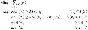
 |
| Figure 24.1. |
| A generic GPU hardware architecture.
|
24.3. Algorithms, Implementations, and Evaluations
24.3.1. Gate-Level Task Scheduling
We describe the gate-level task scheduling in the context of topological order traversal of the circuit. The techniques for reverse topological order traversal are almost the same. In a topological order
traversal, a gate is a
processed gate
if the computation of delay/power for all of its implementations is completed. A gate is called a
current gate
if all of its fan-in gates are processed gates. We term a gate as a
prospective gate
when all of its fan-in gates are either current gates or processed gates. In GPU-based parallel computing, multiple current gates can be processed at the same time because there is no interdependency among their computations. Current gates are also called
independent current gates
(ICG) because there is no computational interdependency among them. Because of the restriction of GPU computing bandwidth, the number of current gates that can be processed at the same time is limited. A critical problem here is how to select a subset of independent current gates for parallel processing. This subset is designated as
concurrent gate group
, which has a maximum allowed size.
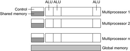
The way of forming a concurrent gate group may greatly affect the efficiency of utilizing the GPU-based parallelism. This can be illustrated by the example in
Figure 24.2
. In
Figure 24.2
, the processed gates, independent current gates, and prospective gates are represented by dashed, gray, and white rectangles, respectively. If the maximum group size is four, there could be at least two different ways of forming a concurrent gate group for the scenario of
Figure 24.2(a)
. In
Figure 24.2(b)
, {
G
1,
G
2,
G
3,
G
4} are selected to be the concurrent gate group. After they are processed, any four gates among {
G
5,
G
6,
G
7,
G
8,
G
9} may become the next concurrent gate group. Alternatively, we can choose {
G
2,
G
3,
G
4,
G
5} as in
Figure 24.2(c)
. However, after {
G
2,
G
3,
G
4,
G
5} are processed, we can include at most three gates {
G
1,
G
9,
G
10} for the next concurrent gate group because a fan-in gate for {
G
6,
G
7,
G
8} has not been processed yet. The selection of concurrent gates in
Figure 24.2(c)
is inferior to that in
Figure 24.2(b)
because
Figure 24.2(c)
cannot fully utilize the bandwidth of concurrent group size 4.
 |
| Figure 24.2
Processed gates: dashed rectangles; independent current gates: gray rectangles; prospective gates: solid white rectangles. For the scenario in (a), one can choose at most four independent current gates for the parallel processing. In (b): if
G
1,
G
2,
G
3, and
G
4 are selected, we may choose another four gates in
G
5,
G
6,
G
7,
G
8, and
G
9 for the next parallel processing. In (c): if
G
2,
G
3,
G
4, and
G
5 are selected, only three independent current gates
G
1,
G
9, and
G
10 are available for the next parallel processing.
|
The problem of finding a concurrent gate group among a set of independent current gates can be formulated as a max-throughput problem, which maximizes the minimum size of all concurrent gate groups. The max-throughput problem is very difficult to solve. Therefore, we will focus on a reduced problem: max-succeeding-group. Given a set of independent current gates, the max-succeeding-group problem asks to choose a subset of them as the concurrent gate group such that the size of the succeeding independent gate group is maximized. We show in the last section of this chapter that the max-succeeding-group problem is NP-complete.
Because the max-succeeding-group problem is NP-complete, we propose a linear-time heuristic to solve it. This heuristic iteratively examines the prospective gates and puts a few independent current gates into the concurrent gate group. For each prospective gate, we check its fan-in gates that are independent current gates. The number of such fan-in gates is called ICG (independent current gate) fan-in size. In each iteration, the prospective gate with the minimum ICG fan-in size is selected. Then, all of its ICG fan-in gates are put into the concurrent gate group. Afterward, the selected prospective gate will no longer be considered in subsequent iterations. At the same time, the selected ICG fan-in gates are not counted in the ICG fan-in size of the remaining prospective gates.
In the example in
Figure 24.2
, the prospective gate with the minimum ICG fan-in size is
G
9. When it is selected, gate
G
3 is put into the concurrent gate group. Then, the ICG fan-in size of
G
7 becomes 1, which is the minimum. This requires gate
G
1 to be put into the concurrent gate group. Next, any two of
G
2,
G
4, and
G
5 can be selected to form the concurrent gate group of size four.
Here is the rationale behind the heuristic. The maximum allowed size of a concurrent gate group can be treated as a budget. The goal is to maximize the number of succeeding ICGs. If a prospective gate has a small ICG fan-in size, selecting its ICG fan-in gates can increase the number of succeeding ICGs with the minimum usage of concurrent gate group budget.
This heuristic is performed on the CPU once. The result, which is the gate-level scheduling, is saved because the same schedule is employed repeatedly in the traversals of the JRR algorithm (see Section 2). The pseudocode for the concurrent gate selection heuristic is given in
Algorithm 2
. The minimum ICG fan-in size is updated each time an ICG fan-in size is updated, so the computation time is dominated by fan-in size updating. If the maximum fan-in size among all gates is
F
i
, each gate can be updated on its ICG fan-in size for at most
F
i
times. Thus, the time complexity of this heuristic is
O
(|
V
|
F
i
), where
V
denotes the set of nodes in the circuit.

24.3.2. Parallel Gate Implementation Evaluation
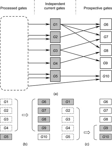
When processing a gate, we need to evaluate all of its implementations. It is not difficult to see that the evaluations for different implementations of the same gate are independent of each other. Therefore, we can allocate these evaluations into multiple threads without worrying about interdependence. These evaluations include a few common computations: the timing and power estimation for each implementation. Different implementations of the same gate also share some common data such as the parasitics of the fan-in and fan-out. According to this observation, the evaluations of implementations for the same gate are assigned to the same thread block and the same multiprocessor. Because all the ALUs of the same multiprocessor have access to a fast on-chip shared memory (see
Figure 24.3
), the shared data can be saved in the shared memory to reduce memory access time. Because the evaluation for an implementation of a gate involves computing it with all the implementations of gates on its fan-in.
Therefore, the number of parallel threads needed in one gate's implementation evaluation is the square of the number of implementations for each gate. For example, in the experiments in the Final Evaluation section, each gate has 24 possible implementations (4
V
t
levels and 6 sizes); thus, there are 576 threads in a thread block.
 |
| Figure 24.3
A multiprocessor with on-chip shared memory. Device memory is connected to the processors through on-chip caches.
|
In order to facilitate simultaneous memory access, the shared memory is usually divided into equal-sized banks. Memory requests on addresses that fall in different banks are able to be fulfilled simultaneously, while requested addresses falling in the same bank cause a bank conflict and the conflicting requests have to be serialized. In order to reduce the chance of bank conflict and avoid the cost of serialized access, we store all information of a gate in the same bank and separate it from that of other gates in other banks.
GPU global memory often has a memory-coalescing mechanism for improved access efficiency. When the data of connected gates in the circuit are saved to adjacent locations in the global memory, memory access requests from different threads in a warp would have a greater chance to be coalesced, and the access latency is thereby reduced. However, because of complex multiple-multiple connections between gates in the circuit, it is difficult to achieve efficient coalesced memory access. Therefore, we employ simple random memory access in this work.
GPU global memory contains a constant memory, which is a read-only region. This constant memory can be accessed by all ALUs through a constant cache (see
Figure 24.3
), which approximately halves the access latency if there is a hit in the cache. We save cell library data, which are constant, in the constant memory so that the data access time can be largely reduced.
Loading the kernel function to GPU can be very time-consuming. Sometimes, the loading time is comparable to time of all computations and memory access for one gate. Therefore, it is highly desirable to reduce the number of calls to the kernel function. Because the computation operations for all gates are the same, we load the computation instructions only once and apply them to all of the gates in the circuit. This is made possible by the fine-grained parallel threads and the precomputed gate-level task schedule (see
Section 3.3
). In other words, the gate-level task schedule is computed before the circuit optimization and saved in the GPU global memory. Once the kernel function is called, the optimization follows the schedule saved on GPU, and no kernel reloading is needed.
To reduce the idle time of the multiprocessors during memory access, we assign multiple thread blocks to a multiprocessor for concurrent execution. This arrangement has a positive impact on the performance because memory access takes a large portion of the total execution time of the kernel function.
24.4. Final Evaluation
In our experiment, the test cases are the ISCAS85 combinational circuits. They are synthesized by SIS
[8]
and their global placement is obtained by mPL
[9]
. The global placement is for the sake of including wire delay in the timing analysis. The cell library is based on 70 nm technology. Each gate has six different sizes and four
V
t
levels so that it has 24 options of implementation.
In order to test the runtime speedup of our parallel techniques, we compare our parallel version of the JRR algorithm
[5]
with its original sequential implementation. Regarding solution quality, we compare the results with another previous work
[6]
in addition to ensuring that the parallel JRR solutions are identical with those of sequential JRR. The method of Nguyen
et al
.
[6]
starts with gate sizing that
maximizes timing slack. Then, the slack is allocated to each gate using a linear programming guided by delay/power sensitivity. The slack allocated to each gate is further converted to power reduction by greedily choosing a gate implementation. We call this a method based on slack allocation (SA). The problem formulation for all these methods is to minimize total power dissipation subject to timing constraints. The power dissipation here includes both dynamic and leakage power. The timing evaluation accounts for both gate and wire delay. Because we do not have lookup table-based timing and power information for the cell library, we use the analytical model for power
[5]
and the Elmore model for delay computation. However, the JRR algorithm and our parallel techniques can be easily applied with lookup table-based models.
The SA method and sequential JRR algorithm are implemented in C++. The parallel JRR implementation includes two parts: one part is in C++ and runs on the host CPU; the other part runs on the GPU through CUDA (Compute Unified Device Architecture), a parallel programming model and interface developed by NVIDIA
[7]
. The major components of the parallel programming model and software environment include thread groups, shared memory, and thread synchronization. The experiment was performed on a Windows XP-based machine with an Intel core 2 duo CPU of 2.66GHz and 2GB of memory. The GPU is NVIDIA GeForce 9800GT, which has 14 multiprocessors, and each multiprocessor has eight ALUs. The GPU card has 512MB of off-chip memory. We set the maximum number of gates being parallel processed to four. Therefore, at most, 96 gate implementations are evaluated at one time.
The main results are listed in
Table 24.1
. Because all of these methods can satisfy the timing constraints, timing results are not included in the table. The solution quality can be evaluated by the results of power dissipation. One can see that JRR can reduce power by about 24% on average when compared with SA
[6]
. The parallel JRR achieves exactly the same power as the sequential JRR. Our parallel techniques provide runtime speedup from 10× to 56×. One can see that the speedup tends to be more significant when the circuit size grows. One of the reasons is that both small and large circuits have similar overhead for setup.
| Circuit | No. gates | SA [6] | Sequential JRR [5] | Parallel JRR | |||
|---|---|---|---|---|---|---|---|
| Power | Runtime | Power | Runtime | Runtime | Speedup | ||
| c432 | 289 | 703 | 1.7 | 701 | 3.25 | 0.317 | 10× |
| c499 | 539 | 1669 | 4.9 | 1590 | 6.27 | 0.295 | 21× |
| c880 | 340 | 1817 | 5.1 | 1050 | 3.61 | 0.328 | 11× |
| c1355 | 579 | 1385 | 3.3 | 1076 | 7.36 | 0.218 | 34× |
| c1908 | 722 | 2502 | 10.7 | 2296 | 9.20 | 0.327 | 28× |
| c2670 | 1082 | 3412 | 18.6 | 2509 | 15.70 | 0.376 | 42× |
| c3540 | 1208 | 4645 | 22.3 | 3830 | 21.30 | 0.515 | 41× |
| c5315 | 2440 | 8406 | 26.8 | 5023 | 64.88 | 1.156 | 56× |
| c6288 | 2342 | 13,685 | 19.2 | 12,356 | 53.47 | 1.295 | 41× |
| c7552 | 3115 | 9510 | 46.1 | 5949 | 67.44 | 1.595 | 42× |
| Average | 4773 | 15.87 | 3638 | 25.25 | 0.64 | 39× | |
| Norm. | 1.0 | 0.76 | |||||
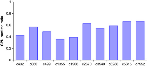
Figure 24.4
shows the ratio between the GPU runtime and the total runtime. Here, the GPU runtime is the runtime of the code on GPU after it is parallelized from a part of the sequential code. The ratio is mostly between 0.4 and 0.6 among all circuits, which means a majority of the sequential runtime is parallelized into GPU computing. Usually, larger circuits have higher GPU runtime percentage. This may be due to the higher parallel efficiency of larger circuits.
 |
| Figure 24.4
The ratio of GPU runtime over overall runtime.
|
In
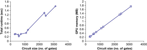
Figure 24.5
, the total runtime and GPU memory usage versus circuit size are plotted to show the runtime and memory scalability of our techniques. The main trend of the runtime curve indicates a linear dependence on circuit size. There are a few nonmonotone parts in the curve that can be explained by the fact that the runtime depends on not only the circuit size but also circuit topology. The memory curve exhibits a strong linear relationship with circuit size. At least for ISCAS85 benchmark circuits, we can conclude that our techniques scale well on both runtime and memory.
 |
| Figure 24.5
Runtime and GPU memory scalability.
|
It has long been a challenge to optimize a combinational circuit in a systematic, yet fast manner owing to its topological reconvergence and large size. A recent progress
[5]
suggests an effective solution to the reconvergence problem. This work addresses the large problem size by exploiting GPU-based parallelism. The proposed parallel techniques are integrated with the state-of-the-art gate sizing and
V
t
assignment algorithm
[5]
. These techniques and the integration effectively solve the challenge of combinational circuit optimization. A circuit with thousands of gates can be optimized with high quality in less than 2 seconds. The parallel techniques provide up to 56× runtime speedup. They also show an appealing trend that the speedup is more significant on large circuits. In the future, we will test these techniques on larger circuits, for example, circuits with hundreds of thousands of gates.
The problem of simultaneous gate sizing and
V
t
assignment is used in this work as an example to demonstrate the application of our GPU-based parallelization techniques. However, more general problems in circuit optimization can be solved by these techniques in combination with the optimization algorithm in
[5]
. Candidate problems, such as technology mapping, voltage assignment, and cell placement, will be explored with the method in future.
NP-Completeness
The NP-completeness of
max-succeeding-group
is proved by reducing the
CLIQUE
problem to an auxiliary problem
MIN-EDGECOVER
, which in turn is reduced to
MIN-DEPCOVER
. Then, we show that MIN-DEPCOVER is equivalent to max-succeeding-group.
Before getting into the first part of our proof, we introduce the concept of edge cover. An edge is covered by a node, if the node is its source or sink. The problem MIN-EDGECOVER asks if
b
nodes from the node set
V
in a graph
G
(V
,
E
) can be selected, such that the number of edges covered by the nodes is at most
a
.
Lemma 1
MIN-EDGECOVER
is NP-complete
.
Proof
First, MIN-EDGECOVER ∈ NP, because checking if a set of
b
nodes covers at most
a
edges takes linear time.
Second, MIN-EDGECOVER is NP-hard, because CLIQUE is polynomial-time reducible to MIN-EDGECOVER, i.e., CLIQUE ≤
P
MIN-EDGECOVER. We construct a function to transform a CLIQUE problem to a MIN-EDGECOVER problem. For a problem that asks if a
b
-node complete subgraph can be found in
G
(V
,
E
), the corresponding MIN-EDGECOVER problem is whether there exists a set of |
V
| −
b
nodes in
G
(V
,
E
) that covers at most |
E
| −
b
(b
− 1)/2 edges. If the answer to the first question is true, then the |
V
| −
b
nodes apart from the
b
nodes in the complete subgraph found in the first question are nodes that cover the |
E
| −
b
(b
− 1)/2 edges outside the complete subgraph. In this case, the answer to the second question is also true. On the other hand, if the answer to the second question is true, then at least
b
(b
− 1)/2 edges other than the |
E
| −
b
(b
− 1)/2 edges found in second question are between the rest
b
nodes. Then, the
b
nodes make a complete graph. Thus, the answer to the first question is true. Therefore, the answer to each of the two aforementioned problems is true if and only if the answer to the other is positive, too.
Because of the simple arithmetic calculation, the transform of the aforementioned reduction clearly runs in
O
(1) time. Therefore, CLIQUE ≤
P
MIN-EDGECOVER.
Next, in the second part of our proof, we show that MIN-EDGECOVER is polynomial-time reducible to the problem MIN-DEPCOVER, which is equivalent to MAX-INDEPSET. An independent graph is a directed graph
G
(V
,
E
′) with two sets of nodes
V
1
and
V
2
(V
=
V
1
⋃
V
2
,
V
1
⋂
V
2
= ∅), and every edge
e
′ ∈
E
′ originates from a node in
V
1
and ends at a node in
V
2
. A node
v
2
in
V
2
is said to be dependently covered by a node
v
1
in
V
1
, if there is an edge from
v
1
to
v
2
. MIN-DEPCOVER asks if a set of
b
nodes can be selected from
V
1
, so that at most
a
nodes in
V
2
are dependently covered.
Lemma 2
MIN-DEPCOVER
is NP-complete.
Proof
First, MIN-DEPCOVER ∈ NP, because checking if a set of
b
nodes in
V
1
dependently cover at most
a
nodes in
V
2
takes polynomial time.
Second, we verify that MIN-DEPCOVER is NP-hard by showing MIN-EDGECOVER ≤
P
MIN-DEPCOVER. We transform any given MIN-EDGECOVER problem on
G
(V
,
E
) into a MIN-DEPCOVER problem on
G
(V
1
⋃
V
2
,
E
′). Each node in
V
corresponds to a node in
V
1
, and each edge in
E
corresponds to a node in
V
2
. An edge
e
′ ∈
E
′ from node
v
1
∈
V
1
to
v
2
∈
V
2
exists if and only if the node
v
corresponding to
v
1
is adjacent to the edge
e
corresponding to
v
2
. If the answer to the first question is true, then there are
b
nodes in
V
1
that dependently cover at most
a
nodes in
V
2
, therefore, the answer to the second question is true, too. And vice versa, if the answer to the second question is true, then there are
b
nodes in
V
that cover at most
a
edges corresponding to
a
nodes in
V
2
. So the answer to the first question is true. Therefore, each of the positive answers to the two problems holds if and only if the other one holds.
During the construction of the corresponding MIN-DEPCOVER problem, given a MIN-EDGECOVER problem, going through every edge in
G
(V
,
E
) and its adjacent nodes takes
O
(E
) time. So the transform takes polynomial time. Consequently, MIN-EDGECOVER ≤
P
MIN-DEPCOVER.
By the two steps of reasoning that we just described, it is proved that MIN-DEPCOVER problem is NP-complete.
In the final part of our proof, we show that max-succeeding-group problem is NP-complete. Before getting into it, we review the concept in max-succeeding-group problem. The decision problem of max-succeeding-group asks if a set of
b
gates from current gate group can be chosen as concurrent gate group so that the size of the succeeding independent group is at least
a
.
Theorem 1
max-succeeding-group
is NP-complete
.
Proof
First, max-succeeding-group ∈ NP because it takes polynomial time to check if a set of
b
independent gates enable at least
a
prospective gates to become independent gates.
Second, we verify that max-succeeding-group is NP-hard by showing MIN-DEPCOVER ≤
P
max-succeeding-group. It is true simply because max-succeeding-group is equivalent to MIN-DEPCOVER. The situation that at least
a
gates in the prospective group are made independent by selecting
b
gates from the independent current set is the same as the situation that at most |
prospective_group
| –
a
gates in the prospective group are prevented from becoming independent gates by excluding |
independent_group
| –
b
independent gates from entering the concurrent group. The two aforementioned statements above are sufficient and necessary conditions to each other because they are equivalent.
Clearly, the preceding transform takes
O
(1) time; therefore, MIN-DEPCOVER ≤
P
max-succeeding-group.
In fact, the NP-completeness of MAX-THROUGHPUT can be verified by a straightforward polynomial-time transform that reduces max-succeeding-group to MAX-THROUGHPUT.
References
[1]
O. Coudert,
Gate sizing for constrained delay/power/area optimization
,
IEEE Trans. Very Large Scale Integr. Syst.
5
(4
) (1997
)
465
–
472
.
[2]
Z. Feng, P. Li,
Multigrid on GPU: tackling power grid analysis on parallel SIMT platforms
,
In:
ICCAD ’08: Proceedings of the 2008 IEEE/ACM International Conference on Computer-Aided Design
(2008
)
IEEE Press
,
Piscataway, NJ
, pp.
647
–
654
.
[3]
K. Gulati, S. Khatri,
Towards acceleration of fault simulation using graphics processing units
,
In:
DAC ’08: Proceedings of the 45th Annual Design Automation Conference
(2008
)
ACM
,
New York
, pp.
822
–
827
.
[4]
J. Owens, D. Luebke et al., A survey of general-purpose computation on graphics hardware, in: Eurographics ’05: Proceedings of 2005 Eurographics, Eurographics Association, 1207 Geneve, Switzerland.
[5]
Y. Liu, J. Hu, A new algorithm for simultaneous gate sizing and threshold voltage assignment, in: ISPD ’09: Proceedings of the 2009 International Symposium on Physical Design, ACM, New York, pp. 27–34.
[6]
D. Nguyen, A. Davare,
et al.
,
Minimization of dynamic and static power through joint assignment of threshold voltages and sizing optimization
,
In:
ISLPED ’03: Proceedings of the 2003 International Symposium on Low Power Electronics and Design
(2003
)
ACM
,
New York
, pp.
158
–
163
.
[7]
NVIDIA CUDA homepage,
http://www.nvidia.com/
.
[8]
E.M. Sentovich,
SIS: A System for Sequential Circuit Synthesis, Memorandum No. UCB/ERL M92/41, UCB Memorandum
. (1992
)
University of California
,
Berkeley
.
[9]
UCLA. CPMO-constrained placement by multilevel optimization, University of California at Los Angeles,
http://ballade.cs.ucla.edu/cpmo
.
[10]
L. Van Ginneken,
Buffer placement in distributed RC-tree networks for minimal elmore delay
,
In:
ISCS ’90: Proceedings of the 1990 International Symposium on Circuits and Systems
(1990
)
IEEE Press
,
Piscataway, NJ
.
[11]
T.-H. Wu, A. Davoodi,
Pars: fast and near-optimal grid-based cell sizing for library-based design
,
In:
ICCAD ’08: Proceedings of the 2008 IEEE/ACM International Conference on Computer-Aided Design
(2008
)
IEEE Press
,
Piscataway, NJ
, pp.
107
–
111
.
..................Content has been hidden....................
You can't read the all page of ebook, please click here login for view all page.