
3
Sequential Logic Design
3.1 Introduction
In the last chapter, we showed how to analyze and design combinational logic. The output of combinational logic depends only on current input values. Given a specification in the form of a truth table or Boolean equation, we can create an optimized circuit to meet the specification.
In this chapter, we will analyze and design sequential logic. The outputs of sequential logic depend on both current and prior input values. Hence, sequential logic has memory. Sequential logic might explicitly remember certain previous inputs, or it might distill the prior inputs into a smaller amount of information called the state of the system. The state of a digital sequential circuit is a set of bits called state variables that contain all the information about the past necessary to explain the future behavior of the circuit.
The chapter begins by studying latches and flip-flops, which are simple sequential circuits that store one bit of state. In general, sequential circuits are complicated to analyze. To simplify design, we discipline ourselves to build only synchronous sequential circuits consisting of combinational logic and banks of flip-flops containing the state of the circuit. The chapter describes finite state machines, which are an easy way to design sequential circuits. Finally, we analyze the speed of sequential circuits and discuss parallelism as a way to increase speed.
3.2 Latches and Flip-Flops
The fundamental building block of memory is a bistable element, an element with two stable states. Figure 3.1(a) shows a simple bistable element consisting of a pair of inverters connected in a loop. Figure 3.1(b) shows the same circuit redrawn to emphasize the symmetry. The inverters are cross-coupled, meaning that the input of I1 is the output of I2 and vice versa. The circuit has no inputs, but it does have two outputs, Q and ![]() Analyzing this circuit is different from analyzing a combinational circuit because it is cyclic: Q depends on
Analyzing this circuit is different from analyzing a combinational circuit because it is cyclic: Q depends on ![]() , and
, and ![]() depends on Q.
depends on Q.

Figure 3.1 Cross-coupled inverter pair
Consider the two cases, Q is 0 or Q is 1. Working through the consequences of each case, we have:
Just as Y is commonly used for the output of combinational logic, Q is commonly used for the output of sequential logic.
![]() Case I: Q = 0
Case I: Q = 0
As shown in Figure 3.2(a), I2 receives a FALSE input, Q, so it produces a TRUE output on ![]() I1 receives a TRUE input,
I1 receives a TRUE input, ![]() , so it produces a FALSE output on Q. This is consistent with the original assumption that Q = 0, so the case is said to be stable.
, so it produces a FALSE output on Q. This is consistent with the original assumption that Q = 0, so the case is said to be stable.
Figure 3.2 Bistable operation of cross-coupled inverters
![]() Case II: Q = 1
Case II: Q = 1
As shown in Figure 3.2(b), I2 receives a TRUE input and produces a FALSE output on ![]() I1 receives a FALSE input and produces a TRUE output on Q. This is again stable.
I1 receives a FALSE input and produces a TRUE output on Q. This is again stable.
Because the cross-coupled inverters have two stable states, Q = 0 and Q = 1, the circuit is said to be bistable. A subtle point is that the circuit has a third possible state with both outputs approximately halfway between 0 and 1. This is called a metastable state and will be discussed in Section 3.5.4.
An element with N stable states conveys log2N bits of information, so a bistable element stores one bit. The state of the cross-coupled inverters is contained in one binary state variable, Q. The value of Q tells us everything about the past that is necessary to explain the future behavior of the circuit. Specifically, if Q = 0, it will remain 0 forever, and if Q = 1, it will remain 1 forever. The circuit does have another node, ![]() , but
, but ![]() does not contain any additional information because if Q is known,
does not contain any additional information because if Q is known, ![]() is also known. On the other hand,
is also known. On the other hand, ![]() is also an acceptable choice for the state variable.
is also an acceptable choice for the state variable.
When power is first applied to a sequential circuit, the initial state is unknown and usually unpredictable. It may differ each time the circuit is turned on.
Although the cross-coupled inverters can store a bit of information, they are not practical because the user has no inputs to control the state. However, other bistable elements, such as latches and flip-flops, provide inputs to control the value of the state variable. The remainder of this section considers these circuits.
3.2.1 SR Latch
One of the simplest sequential circuits is the SR latch, which is composed of two cross-coupled NOR gates, as shown in Figure 3.3. The latch has two inputs, S and R, and two outputs, Q and ![]() The SR latch is similar to the cross-coupled inverters, but its state can be controlled through the S and R inputs, which set and reset the output Q.
The SR latch is similar to the cross-coupled inverters, but its state can be controlled through the S and R inputs, which set and reset the output Q.
Figure 3.3 SR latch schematic
A good way to understand an unfamiliar circuit is to work out its truth table, so that is where we begin. Recall that a NOR gate produces a FALSE output when either input is TRUE. Consider the four possible combinations of R and S.
![]() Case I: R = 1, S = 0
Case I: R = 1, S = 0
N1 sees at least one TRUE input, R, so it produces a FALSE output on Q. N2 sees both Q and S FALSE, so it produces a TRUE output on ![]()
![]() Case II: R = 0, S = 1
Case II: R = 0, S = 1
N1 receives inputs of 0 and ![]() Because we don’t yet know
Because we don’t yet know ![]() , we can’t determine the output Q. N2 receives at least one TRUE input, S, so it produces a FALSE output on
, we can’t determine the output Q. N2 receives at least one TRUE input, S, so it produces a FALSE output on ![]() Now we can revisit N1, knowing that both inputs are FALSE, so the output Q is TRUE.
Now we can revisit N1, knowing that both inputs are FALSE, so the output Q is TRUE.
![]() Case III: R = 1, S = 1
Case III: R = 1, S = 1
N1 and N2 both see at least one TRUE input (R or S), so each produces a FALSE output. Hence Q and ![]() are both FALSE.
are both FALSE.
![]() Case IV: R = 0, S = 0
Case IV: R = 0, S = 0
N1 receives inputs of 0 and ![]() Because we don’t yet know
Because we don’t yet know ![]() , we can’t determine the output. N2 receives inputs of 0 and Q. Because we don’t yet know Q, we can’t determine the output. Now we are stuck. This is reminiscent of the cross-coupled inverters. But we know that Q must either be 0 or 1. So we can solve the problem by checking what happens in each of these subcases.
, we can’t determine the output. N2 receives inputs of 0 and Q. Because we don’t yet know Q, we can’t determine the output. Now we are stuck. This is reminiscent of the cross-coupled inverters. But we know that Q must either be 0 or 1. So we can solve the problem by checking what happens in each of these subcases.
![]() Case IVa: Q = 0
Case IVa: Q = 0
Because S and Q are FALSE, N2 produces a TRUE output on ![]() , as shown in Figure 3.4(a). Now N1 receives one TRUE input,
, as shown in Figure 3.4(a). Now N1 receives one TRUE input, ![]() , so its output, Q, is FALSE, just as we had assumed.
, so its output, Q, is FALSE, just as we had assumed.

Figure 3.4 Bistable states of SR latch
![]() Case IVb: Q = 1
Case IVb: Q = 1
Because Q is TRUE, N2 produces a FALSE output on ![]() , as shown in Figure 3.4(b). Now N1 receives two FALSE inputs, R and
, as shown in Figure 3.4(b). Now N1 receives two FALSE inputs, R and ![]() , so its output, Q, is TRUE, just as we had assumed.
, so its output, Q, is TRUE, just as we had assumed.
Putting this all together, suppose Q has some known prior value, which we will call Qprev, before we enter Case IV. Qprev is either 0 or 1, and represents the state of the system. When R and S are 0, Q will remember this old value, Qprev, and ![]() will be its complement,
will be its complement, ![]() This circuit has memory.
This circuit has memory.
The truth table in Figure 3.5 summarizes these four cases. The inputs S and R stand for Set and Reset. To set a bit means to make it TRUE. To reset a bit means to make it FALSE. The outputs, Q and ![]() , are normally complementary. When R is asserted, Q is reset to 0 and
, are normally complementary. When R is asserted, Q is reset to 0 and ![]() does the opposite. When S is asserted, Q is set to 1 and
does the opposite. When S is asserted, Q is set to 1 and ![]() does the opposite. When neither input is asserted, Q remembers its old value, Qprev. Asserting both S and R simultaneously doesn’t make much sense because it means the latch should be set and reset at the same time, which is impossible. The poor confused circuit responds by making both outputs 0.
does the opposite. When neither input is asserted, Q remembers its old value, Qprev. Asserting both S and R simultaneously doesn’t make much sense because it means the latch should be set and reset at the same time, which is impossible. The poor confused circuit responds by making both outputs 0.
Figure 3.5 SR latch truth table
The SR latch is represented by the symbol in Figure 3.6. Using the symbol is an application of abstraction and modularity. There are various ways to build an SR latch, such as using different logic gates or transistors. Nevertheless, any circuit element with the relationship specified by the truth table in Figure 3.5 and the symbol in Figure 3.6 is called an SR latch.

Figure 3.6 SR latch symbol
Like the cross-coupled inverters, the SR latch is a bistable element with one bit of state stored in Q. However, the state can be controlled through the S and R inputs. When R is asserted, the state is reset to 0. When S is asserted, the state is set to 1. When neither is asserted, the state retains its old value. Notice that the entire history of inputs can be accounted for by the single state variable Q. No matter what pattern of setting and resetting occurred in the past, all that is needed to predict the future behavior of the SR latch is whether it was most recently set or reset.
3.2.2 D Latch
The SR latch is awkward because it behaves strangely when both S and R are simultaneously asserted. Moreover, the S and R inputs conflate the issues of what and when. Asserting one of the inputs determines not only what the state should be but also when it should change. Designing circuits becomes easier when these questions of what and when are separated. The D latch in Figure 3.7(a) solves these problems. It has two inputs. The data input, D, controls what the next state should be. The clock input, CLK, controls when the state should change.
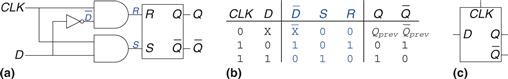
Figure 3.7 D latch: (a) schematic, (b) truth table, (c) symbol
Again, we analyze the latch by writing the truth table, given in Figure 3.7(b). For convenience, we first consider the internal nodes ![]() , S, and R. If CLK = 0, both S and R are FALSE, regardless of the value of D. If CLK = 1, one AND gate will produce TRUE and the other FALSE, depending on the value of D. Given S and R, Q and
, S, and R. If CLK = 0, both S and R are FALSE, regardless of the value of D. If CLK = 1, one AND gate will produce TRUE and the other FALSE, depending on the value of D. Given S and R, Q and ![]() are determined using Figure 3.5. Observe that when CLK = 0, Q remembers its old value, Qprev. When CLK = 1, Q = D. In all cases,
are determined using Figure 3.5. Observe that when CLK = 0, Q remembers its old value, Qprev. When CLK = 1, Q = D. In all cases, ![]() is the complement of Q, as would seem logical. The D latch avoids the strange case of simultaneously asserted R and S inputs.
is the complement of Q, as would seem logical. The D latch avoids the strange case of simultaneously asserted R and S inputs.
Putting it all together, we see that the clock controls when data flows through the latch. When CLK = 1, the latch is transparent. The data at D flows through to Q as if the latch were just a buffer. When CLK = 0, the latch is opaque. It blocks the new data from flowing through to Q, and Q retains the old value. Hence, the D latch is sometimes called a transparent latch or a level-sensitive latch. The D latch symbol is given in Figure 3.7(c).
The D latch updates its state continuously while CLK = 1. We shall see later in this chapter that it is useful to update the state only at a specific instant in time. The D flip-flop described in the next section does just that.
Some people call a latch open or closed rather than transparent or opaque. However, we think those terms are ambiguous—does open mean transparent like an open door, or opaque, like an open circuit?
The precise distinction between flip-flops and latches is somewhat muddled and has evolved over time. In common industry usage, a flip-flop is edge-triggered. In other words, it is a bistable element with a clock input. The state of the flip-flop changes only in response to a clock edge, such as when the clock rises from 0 to 1. Bistable elements without an edge-triggered clock are commonly called latches.
The term flip-flop or latch by itself usually refers to a D flip-flop or D latch, respectively, because these are the types most commonly used in practice.
3.2.3 D FIip-Flop
A D flip-flop can be built from two back-to-back D latches controlled by complementary clocks, as shown in Figure 3.8(a). The first latch, L1, is called the master. The second latch, L2, is called the slave. The node between them is named N1. A symbol for the D flip-flop is given in Figure 3.8(b). When the ![]() output is not needed, the symbol is often condensed as in Figure 3.8(c).
output is not needed, the symbol is often condensed as in Figure 3.8(c).
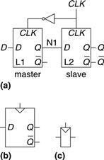
Figure 3.8 D flip-flop: (a) schematic, (b) symbol, (c) condensed symbol
When CLK = 0, the master latch is transparent and the slave is opaque. Therefore, whatever value was at D propagates through to N1. When CLK = 1, the master goes opaque and the slave becomes transparent. The value at N1 propagates through to Q, but N1 is cut off from D. Hence, whatever value was at D immediately before the clock rises from 0 to 1 gets copied to Q immediately after the clock rises. At all other times, Q retains its old value, because there is always an opaque latch blocking the path between D and Q.
In other words, a D flip-flop copies D to Q on the rising edge of the clock, and remembers its state at all other times. Reread this definition until you have it memorized; one of the most common problems for beginning digital designers is to forget what a flip-flop does. The rising edge of the clock is often just called the clock edge for brevity. The D input specifies what the new state will be. The clock edge indicates when the state should be updated.
A D flip-flop is also known as a master-slave flip-flop, an edge-triggered flip-flop, or a positive edge-triggered flip-flop. The triangle in the symbols denotes an edge-triggered clock input. The ![]() output is often omitted when it is not needed.
output is often omitted when it is not needed.
Example 3.1 Flip-Flop Transistor Count
How many transistors are needed to build the D flip-flop described in this section?
Solution
A NAND or NOR gate uses four transistors. A NOT gate uses two transistors. An AND gate is built from a NAND and a NOT, so it uses six transistors. The SR latch uses two NOR gates, or eight transistors. The D latch uses an SR latch, two AND gates, and a NOT gate, or 22 transistors. The D flip-flop uses two D latches and a NOT gate, or 46 transistors. Section 3.2.7 describes a more efficient CMOS implementation using transmission gates.
3.2.4 Register
An N-bit register is a bank of N flip-flops that share a common CLK input, so that all bits of the register are updated at the same time. Registers are the key building block of most sequential circuits. Figure 3.9 shows the schematic and symbol for a four-bit register with inputs D3:0 and outputs Q3:0. D3:0 and Q3:0 are both 4-bit busses.
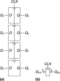
Figure 3.9 A 4-bit register: (a) schematic and (b) symbol
3.2.5 Enabled Flip-Flop
An enabled flip-flop adds another input called EN or ENABLE to determine whether data is loaded on the clock edge. When EN is TRUE, the enabled flip-flop behaves like an ordinary D flip-flop. When EN is FALSE, the enabled flip-flop ignores the clock and retains its state. Enabled flip-flops are useful when we wish to load a new value into a flip-flop only some of the time, rather than on every clock edge.
Figure 3.10 shows two ways to construct an enabled flip-flop from a D flip-flop and an extra gate. In Figure 3.10(a), an input multiplexer chooses whether to pass the value at D, if EN is TRUE, or to recycle the old state from Q, if EN is FALSE. In Figure 3.10(b), the clock is gated. If EN is TRUE, the CLK input to the flip-flop toggles normally. If EN is FALSE, the CLK input is also FALSE and the flip-flop retains its old value. Notice that EN must not change while CLK = 1, lest the flip-flop see a clock glitch (switch at an incorrect time). Generally, performing logic on the clock is a bad idea. Clock gating delays the clock and can cause timing errors, as we will see in Section 3.5.3, so do it only if you are sure you know what you are doing. The symbol for an enabled flip-flop is given in Figure 3.10(c).
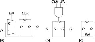
Figure 3.10 Enabled flip-flop: (a, b) schematics, (c) symbol
3.2.6 Resettable Flip-Flop
A resettable flip-flop adds another input called RESET. When RESET is FALSE, the resettable flip-flop behaves like an ordinary D flip-flop. When RESET is TRUE, the resettable flip-flop ignores D and resets the output to 0. Resettable flip-flops are useful when we want to force a known state (i.e., 0) into all the flip-flops in a system when we first turn it on.
Such flip-flops may be synchronously or asynchronously resettable. Synchronously resettable flip-flops reset themselves only on the rising edge of CLK. Asynchronously resettable flip-flops reset themselves as soon as RESET becomes TRUE, independent of CLK.
Figure 3.11(a) shows how to construct a synchronously resettable flip-flop from an ordinary D flip-flop and an AND gate. When ![]() is FALSE, the AND gate forces a 0 into the input of the flip-flop. When
is FALSE, the AND gate forces a 0 into the input of the flip-flop. When ![]() is TRUE, the AND gate passes D to the flip-flop. In this example,
is TRUE, the AND gate passes D to the flip-flop. In this example, ![]() is an active low signal, meaning that the reset signal performs its function when it is 0, not 1. By adding an inverter, the circuit could have accepted an active high reset signal instead. Figures 3.11(b) and 3.11(c) show symbols for the resettable flip-flop with active high reset.
is an active low signal, meaning that the reset signal performs its function when it is 0, not 1. By adding an inverter, the circuit could have accepted an active high reset signal instead. Figures 3.11(b) and 3.11(c) show symbols for the resettable flip-flop with active high reset.
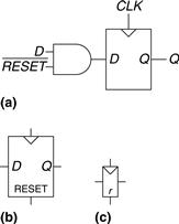
Figure 3.11 Synchronously resettable flip-flop: (a) schematic, (b, c) symbols
Asynchronously resettable flip-flops require modifying the internal structure of the flip-flop and are left to you to design in Exercise 3.13; however, they are frequently available to the designer as a standard component.
As you might imagine, settable flip-flops are also occasionally used. They load a 1 into the flip-flop when SET is asserted, and they too come in synchronous and asynchronous flavors. Resettable and settable flip-flops may also have an enable input and may be grouped into N-bit registers.
3.2.7 Transistor-Level Latch and Flip-Flop Designs*
Example 3.1 showed that latches and flip-flops require a large number of transistors when built from logic gates. But the fundamental role of a latch is to be transparent or opaque, much like a switch. Recall from Section 1.7.7 that a transmission gate is an efficient way to build a CMOS switch, so we might expect that we could take advantage of transmission gates to reduce the transistor count.
A compact D latch can be constructed from a single transmission gate, as shown in Figure 3.12(a). When CLK = 1 and ![]() = 0, the transmission gate is ON, so D flows to Q and the latch is transparent. When CLK = 0 and
= 0, the transmission gate is ON, so D flows to Q and the latch is transparent. When CLK = 0 and ![]() = 1, the transmission gate is OFF, so Q is isolated from D and the latch is opaque. This latch suffers from two major limitations:
= 1, the transmission gate is OFF, so Q is isolated from D and the latch is opaque. This latch suffers from two major limitations:
![]() Floating output node: When the latch is opaque, Q is not held at its value by any gates. Thus Q is called a floating or dynamic node. After some time, noise and charge leakage may disturb the value of Q.
Floating output node: When the latch is opaque, Q is not held at its value by any gates. Thus Q is called a floating or dynamic node. After some time, noise and charge leakage may disturb the value of Q.
![]() No buffers: The lack of buffers has caused malfunctions on several commercial chips. A spike of noise that pulls D to a negative voltage can turn on the nMOS transistor, making the latch transparent, even when CLK = 0. Likewise, a spike on D above VDD can turn on the pMOS transistor even when CLK = 0. And the transmission gate is symmetric, so it could be driven backward with noise on Q affecting the input D. The general rule is that neither the input of a transmission gate nor the state node of a sequential circuit should ever be exposed to the outside world, where noise is likely.
No buffers: The lack of buffers has caused malfunctions on several commercial chips. A spike of noise that pulls D to a negative voltage can turn on the nMOS transistor, making the latch transparent, even when CLK = 0. Likewise, a spike on D above VDD can turn on the pMOS transistor even when CLK = 0. And the transmission gate is symmetric, so it could be driven backward with noise on Q affecting the input D. The general rule is that neither the input of a transmission gate nor the state node of a sequential circuit should ever be exposed to the outside world, where noise is likely.

Figure 3.12 D latch schematic
Figure 3.12(b) shows a more robust 12-transistor D latch used on modern commercial chips. It is still built around a clocked transmission gate, but it adds inverters I1 and I2 to buffer the input and output. The state of the latch is held on node N1. Inverter I3 and the tristate buffer, T1, provide feedback to turn N1 into a static node. If a small amount of noise occurs on N1 while CLK = 0, T1 will drive N1 back to a valid logic value.
Figure 3.13 shows a D flip-flop constructed from two static latches controlled by ![]() and CLK. Some redundant internal inverters have been removed, so the flip-flop requires only 20 transistors.
and CLK. Some redundant internal inverters have been removed, so the flip-flop requires only 20 transistors.
This circuit assumes CLK and ![]() are both available. If not, two more transistors are needed for a CLK inverter.
are both available. If not, two more transistors are needed for a CLK inverter.
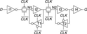
Figure 3.13 D flip-flop schematic
3.2.8 Putting It All Together
Latches and flip-flops are the fundamental building blocks of sequential circuits. Remember that a D latch is level-sensitive, whereas a D flip-flop is edge-triggered. The D latch is transparent when CLK = 1, allowing the input D to flow through to the output Q. The D flip-flop copies D to Q on the rising edge of CLK. At all other times, latches and flip-flops retain their old state. A register is a bank of several D flip-flops that share a common CLK signal.
Example 3.2 Flip-Flop and Latch Comparison
Ben Bitdiddle applies the D and CLK inputs shown in Figure 3.14 to a D latch and a D flip-flop. Help him determine the output, Q, of each device.
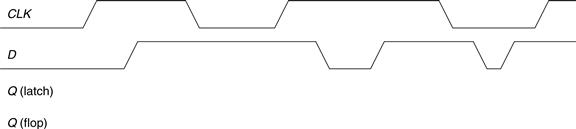
Figure 3.14 Example waveforms
Solution
Figure 3.15 shows the output waveforms, assuming a small delay for Q to respond to input changes. The arrows indicate the cause of an output change. The initial value of Q is unknown and could be 0 or 1, as indicated by the pair of horizontal lines. First consider the latch. On the first rising edge of CLK, D = 0, so Q definitely becomes 0. Each time D changes while CLK = 1, Q also follows. When D changes while CLK = 0, it is ignored. Now consider the flip-flop. On each rising edge of CLK, D is copied to Q. At all other times, Q retains its state.

Figure 3.15 Solution waveforms
3.3 Synchronous Logic Design
In general, sequential circuits include all circuits that are not combinational—that is, those whose output cannot be determined simply by looking at the current inputs. Some sequential circuits are just plain kooky. This section begins by examining some of those curious circuits. It then introduces the notion of synchronous sequential circuits and the dynamic discipline. By disciplining ourselves to synchronous sequential circuits, we can develop easy, systematic ways to analyze and design sequential systems.
3.3.1 Some Problematic Circuits
Example 3.3 Astable Circuits
Alyssa P. Hacker encounters three misbegotten inverters who have tied themselves in a loop, as shown in Figure 3.16. The output of the third inverter is fed back to the first inverter. Each inverter has a propagation delay of 1 ns. Determine what the circuit does.
![]()
Figure 3.16 Three-inverter loop
Solution
Suppose node X is initially 0. Then Y = 1, Z = 0, and hence X = 1, which is inconsistent with our original assumption. The circuit has no stable states and is said to be unstable or astable. Figure 3.17 shows the behavior of the circuit. If X rises at time 0, Y will fall at 1 ns, Z will rise at 2 ns, and X will fall again at 3 ns. In turn, Y will rise at 4 ns, Z will fall at 5 ns, and X will rise again at 6 ns, and then the pattern will repeat. Each node oscillates between 0 and 1 with a period (repetition time) of 6 ns. This circuit is called a ring oscillator.
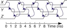
Figure 3.17 Ring oscillator waveforms
The period of the ring oscillator depends on the propagation delay of each inverter. This delay depends on how the inverter was manufactured, the power supply voltage, and even the temperature. Therefore, the ring oscillator period is difficult to accurately predict. In short, the ring oscillator is a sequential circuit with zero inputs and one output that changes periodically.
Example 3.4 Race Conditions
Ben Bitdiddle designed a new D latch that he claims is better than the one in Figure 3.7 because it uses fewer gates. He has written the truth table to find the output, Q, given the two inputs, D and CLK, and the old state of the latch, Qprev. Based on this truth table, he has derived Boolean equations. He obtains Qprev by feeding back the output, Q. His design is shown in Figure 3.18. Does his latch work correctly, independent of the delays of each gate?

Figure 3.18 An improved (?) D latch
Solution
Figure 3.19 shows that the circuit has a race condition that causes it to fail when certain gates are slower than others. Suppose CLK = D = 1. The latch is transparent and passes D through to make Q = 1. Now, CLK falls. The latch should remember its old value, keeping Q = 1. However, suppose the delay through the inverter from CLK to ![]() is rather long compared to the delays of the AND and OR gates. Then nodes N1 and Q may both fall before
is rather long compared to the delays of the AND and OR gates. Then nodes N1 and Q may both fall before ![]() rises. In such a case, N2 will never rise, and Q becomes stuck at 0.
rises. In such a case, N2 will never rise, and Q becomes stuck at 0.
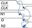
Figure 3.19 Latch waveforms illustrating race condition
This is an example of asynchronous circuit design in which outputs are directly fed back to inputs. Asynchronous circuits are infamous for having race conditions where the behavior of the circuit depends on which of two paths through logic gates is fastest. One circuit may work, while a seemingly identical one built from gates with slightly different delays may not work. Or the circuit may work only at certain temperatures or voltages at which the delays are just right. These malfunctions are extremely difficult to track down.
3.3.2 Synchronous Sequential Circuits
The previous two examples contain loops called cyclic paths, in which outputs are fed directly back to inputs. They are sequential rather than combinational circuits. Combinational logic has no cyclic paths and no races. If inputs are applied to combinational logic, the outputs will always settle to the correct value within a propagation delay. However, sequential circuits with cyclic paths can have undesirable races or unstable behavior. Analyzing such circuits for problems is time-consuming, and many bright people have made mistakes.
To avoid these problems, designers break the cyclic paths by inserting registers somewhere in the path. This transforms the circuit into a collection of combinational logic and registers. The registers contain the state of the system, which changes only at the clock edge, so we say the state is synchronized to the clock. If the clock is sufficiently slow, so that the inputs to all registers settle before the next clock edge, all races are eliminated. Adopting this discipline of always using registers in the feedback path leads us to the formal definition of a synchronous sequential circuit.
Recall that a circuit is defined by its input and output terminals and its functional and timing specifications. A sequential circuit has a finite set of discrete states {S0, S1,…, Sk−1}. A synchronous sequential circuit has a clock input, whose rising edges indicate a sequence of times at which state transitions occur. We often use the terms current state and next state to distinguish the state of the system at the present from the state to which it will enter on the next clock edge. The functional specification details the next state and the value of each output for each possible combination of current state and input values. The timing specification consists of an upper bound, tpcq, and a lower bound, tccq, on the time from the rising edge of the clock until the output changes, as well as setup and hold times, tsetup and thold, that indicate when the inputs must be stable relative to the rising edge of the clock.
tpcq stands for the time of propagation from clock to Q, where Q indicates the output of a synchronous sequential circuit. tccq stands for the time of contamination from clock to Q. These are analogous to tpd and tcd in combinational logic.
The rules of synchronous sequential circuit composition teach us that a circuit is a synchronous sequential circuit if it consists of interconnected circuit elements such that
![]() Every circuit element is either a register or a combinational circuit
Every circuit element is either a register or a combinational circuit
![]() At least one circuit element is a register
At least one circuit element is a register
This definition of a synchronous sequential circuit is sufficient, but more restrictive than necessary. For example, in high-performance microprocessors, some registers may receive delayed or gated clocks to squeeze out the last bit of performance or power. Similarly, some microprocessors use latches instead of registers. However, the definition is adequate for all of the synchronous sequential circuits covered in this book and for most commercial digital systems.
Sequential circuits that are not synchronous are called asynchronous.
A flip-flop is the simplest synchronous sequential circuit. It has one input, D, one clock, CLK, one output, Q, and two states, {0, 1}. The functional specification for a flip-flop is that the next state is D and that the output, Q, is the current state, as shown in Figure 3.20.

Figure 3.20 Flip-flop current state and next state
We often call the current state variable S and the next state variable S′. In this case, the prime after S indicates next state, not inversion. The timing of sequential circuits will be analyzed in Section 3.5.
Two other common types of synchronous sequential circuits are called finite state machines and pipelines. These will be covered later in this chapter.
Example 3.5 Synchronous Sequential Circuits
Which of the circuits in Figure 3.21 are synchronous sequential circuits?
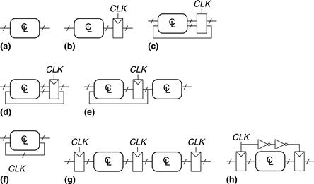
Figure 3.21 Example circuits
Solution
Circuit (a) is combinational, not sequential, because it has no registers. (b) is a simple sequential circuit with no feedback. (c) is neither a combinational circuit nor a synchronous sequential circuit, because it has a latch that is neither a register nor a combinational circuit. (d) and (e) are synchronous sequential logic; they are two forms of finite state machines, which are discussed in Section 3.4. (f) is neither combinational nor synchronous sequential, because it has a cyclic path from the output of the combinational logic back to the input of the same logic but no register in the path. (g) is synchronous sequential logic in the form of a pipeline, which we will study in Section 3.6. (h) is not, strictly speaking, a synchronous sequential circuit, because the second register receives a different clock signal than the first, delayed by two inverter delays.
3.3.3 Synchronous and Asynchronous Circuits
Asynchronous design in theory is more general than synchronous design, because the timing of the system is not limited by clocked registers. Just as analog circuits are more general than digital circuits because analog circuits can use any voltage, asynchronous circuits are more general than synchronous circuits because they can use any kind of feedback. However, synchronous circuits have proved to be easier to design and use than asynchronous circuits, just as digital are easier than analog circuits. Despite decades of research on asynchronous circuits, virtually all digital systems are essentially synchronous.
Of course, asynchronous circuits are occasionally necessary when communicating between systems with different clocks or when receiving inputs at arbitrary times, just as analog circuits are necessary when communicating with the real world of continuous voltages. Furthermore, research in asynchronous circuits continues to generate interesting insights, some of which can improve synchronous circuits too.
3.4 Finite State Machines
Synchronous sequential circuits can be drawn in the forms shown in Figure 3.22. These forms are called finite state machines (FSMs). They get their name because a circuit with k registers can be in one of a finite number (2k) of unique states. An FSM has M inputs, N outputs, and k bits of state. It also receives a clock and, optionally, a reset signal. An FSM consists of two blocks of combinational logic, next state logic and output logic, and a register that stores the state. On each clock edge, the FSM advances to the next state, which was computed based on the current state and inputs. There are two general classes of finite state machines, characterized by their functional specifications. In Moore machines, the outputs depend only on the current state of the machine. In Mealy machines, the outputs depend on both the current state and the current inputs. Finite state machines provide a systematic way to design synchronous sequential circuits given a functional specification. This method will be explained in the remainder of this section, starting with an example.
Moore and Mealy machines are named after their promoters, researchers who developed automata theory, the mathematical underpinnings of state machines, at Bell Labs.
Edward F. Moore (1925–2003), not to be confused with Intel founder Gordon Moore, published his seminal article, Gedanken-experiments on Sequential Machines in 1956. He subsequently became a professor of mathematics and computer science at the University of Wisconsin.
George H. Mealy published A Method of Synthesizing Sequential Circuits in 1955. He subsequently wrote the first Bell Labs operating system for the IBM 704 computer. He later joined Harvard University.

Figure 3.22 Finite state machines: (a) Moore machine, (b) Mealy machine
3.4.1 FSM Design Example
To illustrate the design of FSMs, consider the problem of inventing a controller for a traffic light at a busy intersection on campus. Engineering students are moseying between their dorms and the labs on Academic Ave. They are busy reading about FSMs in their favorite textbook and aren’t looking where they are going. Football players are hustling between the athletic fields and the dining hall on Bravado Boulevard. They are tossing the ball back and forth and aren’t looking where they are going either. Several serious injuries have already occurred at the intersection of these two roads, and the Dean of Students asks Ben Bitdiddle to install a traffic light before there are fatalities.
Ben decides to solve the problem with an FSM. He installs two traffic sensors, TA and TB, on Academic Ave. and Bravado Blvd., respectively. Each sensor indicates TRUE if students are present and FALSE if the street is empty. He also installs two traffic lights, LA and LB, to control traffic. Each light receives digital inputs specifying whether it should be green, yellow, or red. Hence, his FSM has two inputs, TA and TB, and two outputs, LA and LB. The intersection with lights and sensors is shown in Figure 3.23. Ben provides a clock with a 5-second period. On each clock tick (rising edge), the lights may change based on the traffic sensors. He also provides a reset button so that Physical Plant technicians can put the controller in a known initial state when they turn it on. Figure 3.24 shows a black box view of the state machine.
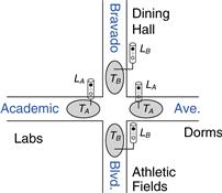
Figure 3.23 Campus map
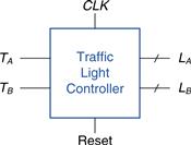
Figure 3.24 Black box view of finite state machine
Ben’s next step is to sketch the state transition diagram, shown in Figure 3.25, to indicate all the possible states of the system and the transitions between these states. When the system is reset, the lights are green on Academic Ave. and red on Bravado Blvd. Every 5 seconds, the controller examines the traffic pattern and decides what to do next. As long as traffic is present on Academic Ave., the lights do not change. When there is no longer traffic on Academic Ave., the light on Academic Ave. becomes yellow for 5 seconds before it turns red and Bravado Blvd.’s light turns green. Similarly, the Bravado Blvd. light remains green as long as traffic is present on the boulevard, then turns yellow and eventually red.
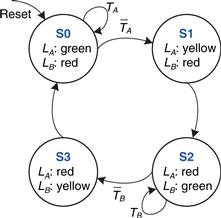
Figure 3.25 State transition diagram
In a state transition diagram, circles represent states and arcs represent transitions between states. The transitions take place on the rising edge of the clock; we do not bother to show the clock on the diagram, because it is always present in a synchronous sequential circuit. Moreover, the clock simply controls when the transitions should occur, whereas the diagram indicates which transitions occur. The arc labeled Reset pointing from outer space into state S0 indicates that the system should enter that state upon reset, regardless of what previous state it was in. If a state has multiple arcs leaving it, the arcs are labeled to show what input triggers each transition. For example, when in state S0, the system will remain in that state if TA is TRUE and move to S1 if TA is FALSE. If a state has a single arc leaving it, that transition always occurs regardless of the inputs. For example, when in state S1, the system will always move to S2. The value that the outputs have while in a particular state are indicated in the state. For example, while in state S2, LA is red and LB is green.
Ben rewrites the state transition diagram as a state transition table (Table 3.1), which indicates, for each state and input, what the next state, S′, should be. Note that the table uses don’t care symbols (X) whenever the next state does not depend on a particular input. Also note that Reset is omitted from the table. Instead, we use resettable flip-flops that always go to state S0 on reset, independent of the inputs.
Table 3.1 State transition table

The state transition diagram is abstract in that it uses states labeled {S0, S1, S2, S3} and outputs labeled {red, yellow, green}. To build a real circuit, the states and outputs must be assigned binary encodings. Ben chooses the simple encodings given in Tables 3.2 and 3.3. Each state and each output is encoded with two bits: S1:0, LA1:0, and LB1:0.
Notice that states are designated as S0, S1, etc. The subscripted versions, S0, S1, etc., refer to the state bits.
Table 3.2 State encoding
| State | Encoding S1:0 |
| S0 | 00 |
| S1 | 01 |
| S2 | 10 |
| S3 | 11 |
Table 3.3 Output encoding
| Output | Encoding L1:0 |
| green | 00 |
| yellow | 01 |
| red | 10 |
Ben updates the state transition table to use these binary encodings, as shown in Table 3.4. The revised state transition table is a truth table specifying the next state logic. It defines next state, S′, as a function of the current state, S, and the inputs.
Table 3.4 State transition table with binary encodings
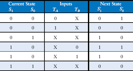
From this table, it is straightforward to read off the Boolean equations for the next state in sum-of-products form.
![]() (3.1)
(3.1)
The equations can be simplified using Karnaugh maps, but often doing it by inspection is easier. For example, the TB and ![]() terms in the
terms in the ![]() equation are clearly redundant. Thus
equation are clearly redundant. Thus ![]() reduces to an XOR operation. Equation 3.2 gives the simplified next state equations.
reduces to an XOR operation. Equation 3.2 gives the simplified next state equations.
![]() (3.2)
(3.2)
Similarly, Ben writes an output table (Table 3.5) indicating, for each state, what the output should be in that state. Again, it is straightforward to read off and simplify the Boolean equations for the outputs. For example, observe that LA1 is TRUE only on the rows where S1 is TRUE.
Table 3.5 Output table

 (3.3)
(3.3)
Finally, Ben sketches his Moore FSM in the form of Figure 3.22(a). First, he draws the 2-bit state register, as shown in Figure 3.26(a). On each clock edge, the state register copies the next state, S′1:0, to become the state S1:0. The state register receives a synchronous or asynchronous reset to initialize the FSM at startup. Then, he draws the next state logic, based on Equation 3.2, which computes the next state from the current state and inputs, as shown in Figure 3.26(b). Finally, he draws the output logic, based on Equation 3.3, which computes the outputs from the current state, as shown in Figure 3.26(c).
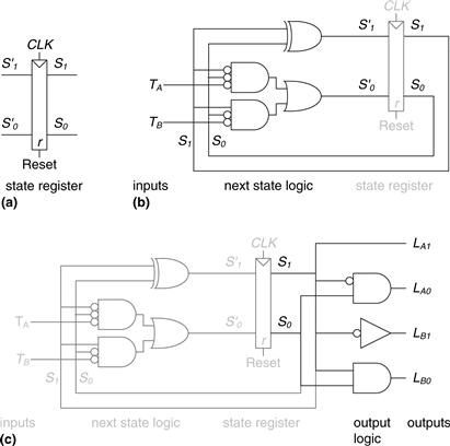
Figure 3.26 State machine circuit for traffic light controller
Figure 3.27 shows a timing diagram illustrating the traffic light controller going through a sequence of states. The diagram shows CLK, Reset, the inputs TA and TB, next state S′, state S, and outputs LA and LB. Arrows indicate causality; for example, changing the state causes the outputs to change, and changing the inputs causes the next state to change. Dashed lines indicate the rising edges of CLK when the state changes.
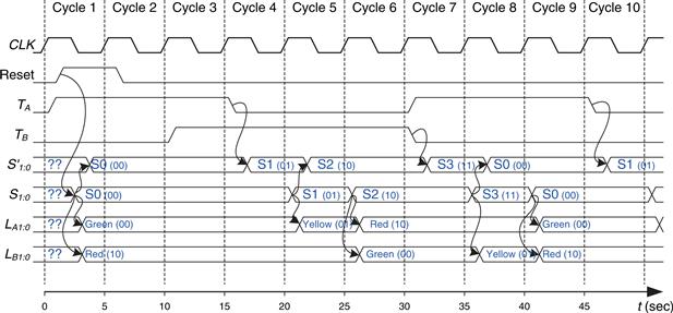
Figure 3.27 Timing diagram for traffic light controller
The clock has a 5-second period, so the traffic lights change at most once every 5 seconds. When the finite state machine is first turned on, its state is unknown, as indicated by the question marks. Therefore, the system should be reset to put it into a known state. In this timing diagram, S immediately resets to S0, indicating that asynchronously resettable flip-flops are being used. In state S0, light LA is green and light LB is red.
This schematic uses some AND gates with bubbles on the inputs. They might be constructed with AND gates and input inverters, with NOR gates and inverters for the non-bubbled inputs, or with some other combination of gates. The best choice depends on the particular implementation technology.
In this example, traffic arrives immediately on Academic Ave. Therefore, the controller remains in state S0, keeping LA green even though traffic arrives on Bravado Blvd. and starts waiting. After 15 seconds, the traffic on Academic Ave. has all passed through and TA falls. At the following clock edge, the controller moves to state S1, turning LA yellow. In another 5 seconds, the controller proceeds to state S2 in which LA turns red and LB turns green. The controller waits in state S2 until all the traffic on Bravado Blvd. has passed through. It then proceeds to state S3, turning LB yellow. 5 seconds later, the controller enters state S0, turning LB red and LA green. The process repeats.
Despite Ben’s best efforts, students don’t pay attention to traffic lights and collisions continue to occur. The Dean of Students next asks him and Alyssa to design a catapult to throw engineering students directly from their dorm roofs through the open windows of the lab, bypassing the troublesome intersection all together. But that is the subject of another textbook.
3.4.2 State Encodings
In the previous example, the state and output encodings were selected arbitrarily. A different choice would have resulted in a different circuit. A natural question is how to determine the encoding that produces the circuit with the fewest logic gates or the shortest propagation delay. Unfortunately, there is no simple way to find the best encoding except to try all possibilities, which is infeasible when the number of states is large. However, it is often possible to choose a good encoding by inspection, so that related states or outputs share bits. Computer-aided design (CAD) tools are also good at searching the set of possible encodings and selecting a reasonable one.
One important decision in state encoding is the choice between binary encoding and one-hot encoding. With binary encoding, as was used in the traffic light controller example, each state is represented as a binary number. Because K binary numbers can be represented by log2K bits, a system with K states only needs log2K bits of state.

In one-hot encoding, a separate bit of state is used for each state. It is called one-hot because only one bit is “hot” or TRUE at any time. For example, a one-hot encoded FSM with three states would have state encodings of 001, 010, and 100. Each bit of state is stored in a flip-flop, so one-hot encoding requires more flip-flops than binary encoding. However, with one-hot encoding, the next-state and output logic is often simpler, so fewer gates are required. The best encoding choice depends on the specific FSM.
Example 3.6 FSM State Encoding
A divide-by-N counter has one output and no inputs. The output Y is HIGH for one clock cycle out of every N. In other words, the output divides the frequency of the clock by N. The waveform and state transition diagram for a divide-by-3 counter is shown in Figure 3.28. Sketch circuit designs for such a counter using binary and one-hot state encodings.
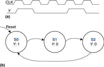
Figure 3.28 Divide-by-3 counter (a) waveform and (b) state transition diagram
Solution
Tables 3.6 and 3.7 show the abstract state transition and output tables before encoding.
Table 3.6 Divide-by-3 counter state transition table
| Current State | Next State |
| S0 | S1 |
| S1 | S2 |
| S2 | S0 |
Table 3.7 Divide-by-3 counter output table
| Current State | Output |
| S0 | 1 |
| S1 | 0 |
| S2 | 0 |
Table 3.8 compares binary and one-hot encodings for the three states.
Table 3.8 One-hot and binary encodings for divide-by-3 counter

The binary encoding uses two bits of state. Using this encoding, the state transition table is shown in Table 3.9. Note that there are no inputs; the next state depends only on the current state. The output table is left as an exercise to the reader. The next-state and output equations are:
![]() (3.4)
(3.4)
![]() (3.5)
(3.5)
Table 3.9 State transition table with binary encoding
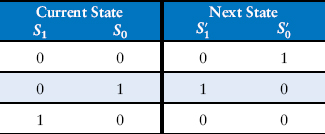
The one-hot encoding uses three bits of state. The state transition table for this encoding is shown in Table 3.10 and the output table is again left as an exercise to the reader. The next-state and output equations are as follows:
![]() (3.6)
(3.6)
![]() (3.7)
(3.7)
Table 3.10 State transition table with one-hot encoding

Figure 3.29 shows schematics for each of these designs. Note that the hardware for the binary encoded design could be optimized to share the same gate for Y and S′0. Also observe that the one-hot encoding requires both settable (s) and resettable (r) flip-flops to initialize the machine to S0 on reset. The best implementation choice depends on the relative cost of gates and flip-flops, but the one-hot design is usually preferable for this specific example.
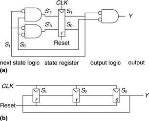
Figure 3.29 Divide-by-3 circuits for (a) binary and (b) one-hot encodings
A related encoding is the one-cold encoding, in which K states are represented with K bits, exactly one of which is FALSE.
3.4.3 Moore and Mealy Machines
So far, we have shown examples of Moore machines, in which the output depends only on the state of the system. Hence, in state transition diagrams for Moore machines, the outputs are labeled in the circles. Recall that Mealy machines are much like Moore machines, but the outputs can depend on inputs as well as the current state. Hence, in state transition diagrams for Mealy machines, the outputs are labeled on the arcs instead of in the circles. The block of combinational logic that computes the outputs uses the current state and inputs, as was shown in Figure 3.22(b).
An easy way to remember the difference between the two types of finite state machines is that a Moore machine typically has more states than a Mealy machine for a given problem.
Example 3.7 Moore Versus Mealy Machines
Alyssa P. Hacker owns a pet robotic snail with an FSM brain. The snail crawls from left to right along a paper tape containing a sequence of 1’s and 0’s. On each clock cycle, the snail crawls to the next bit. The snail smiles when the last two bits that it has crawled over are, from left to right, 01. Design the FSM to compute when the snail should smile. The input A is the bit underneath the snail’s antennae. The output Y is TRUE when the snail smiles. Compare Moore and Mealy state machine designs. Sketch a timing diagram for each machine showing the input, states, and output as Alyssa’s snail crawls along the sequence 0100110111.
Solution
The Moore machine requires three states, as shown in Figure 3.30(a). Convince yourself that the state transition diagram is correct. In particular, why is there an arc from S2 to S1 when the input is 0?
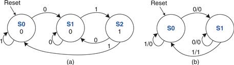
Figure 3.30 FSM state transition diagrams: (a) Moore machine, (b) Mealy machine
In comparison, the Mealy machine requires only two states, as shown in Figure 3.30(b). Each arc is labeled as A/Y. A is the value of the input that causes that transition, and Y is the corresponding output.
Tables 3.11 and 3.12 show the state transition and output tables for the Moore machine. The Moore machine requires at least two bits of state. Consider using a binary state encoding: S0 = 00, S1 = 01, and S2 = 10. Tables 3.13 and 3.14 rewrite the state transition and output tables with these encodings.
Table 3.11 Moore state transition table
| Current State S |
Input A |
Next State S′ |
| S0 | 0 | S1 |
| S0 | 1 | S0 |
| S1 | 0 | S1 |
| S1 | 1 | S2 |
| S2 | 0 | S1 |
| S2 | 1 | S0 |
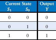
Table 3.12 Moore output table
| Current State S |
Output Y |
| S0 | 0 |
| S1 | 0 |
| S2 | 1 |
Table 3.13 Moore state transition table with state encodings

Table 3.14 Moore output table with state encodings
From these tables, we find the next state and output equations by inspection. Note that these equations are simplified using the fact that state 11 does not exist. Thus, the corresponding next state and output for the non-existent state are don’t cares (not shown in the tables). We use the don’t cares to minimize our equations.
![]() (3.8)
(3.8)
![]() (3.9)
(3.9)
Table 3.15 shows the combined state transition and output table for the Mealy machine. The Mealy machine requires only one bit of state. Consider using a binary state encoding: S0 = 0 and S1 = 1. Table 3.16 rewrites the state transition and output table with these encodings.
Table 3.15 Mealy state transition and output table
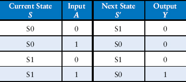
Table 3.16 Mealy state transition and output table with state encodings

From these tables, we find the next state and output equations by inspection.
![]() (3.10)
(3.10)
![]() (3.11)
(3.11)
The Moore and Mealy machine schematics are shown in Figure 3.31. The timing diagrams for each machine are shown in Figure 3.32 (see page 135). The two machines follow a different sequence of states. Moreover, the Mealy machine’s output rises a cycle sooner because it responds to the input rather than waiting for the state change. If the Mealy output were delayed through a flip-flop, it would match the Moore output. When choosing your FSM design style, consider when you want your outputs to respond.
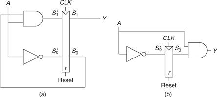
Figure 3.31 FSM schematics for (a) Moore and (b) Mealy machines
Figure 3.32 Timing diagrams for Moore and Mealy machines
3.4.4 Factoring State Machines
Designing complex FSMs is often easier if they can be broken down into multiple interacting simpler state machines such that the output of some machines is the input of others. This application of hierarchy and modularity is called factoring of state machines.
Example 3.8 Unfactored and Factored State Machines
Modify the traffic light controller from Section 3.4.1 to have a parade mode, which keeps the Bravado Boulevard light green while spectators and the band march to football games in scattered groups. The controller receives two more inputs: P and R. Asserting P for at least one cycle enters parade mode. Asserting R for at least one cycle leaves parade mode. When in parade mode, the controller proceeds through its usual sequence until LB turns green, then remains in that state with LB green until parade mode ends.
First, sketch a state transition diagram for a single FSM, as shown in Figure 3.33(a). Then, sketch the state transition diagrams for two interacting FSMs, as shown in Figure 3.33(b). The Mode FSM asserts the output M when it is in parade mode. The Lights FSM controls the lights based on M and the traffic sensors, TA and TB.
Figure 3.33 (a) single and (b) factored designs for modified traffic light controller FSM
Solution
Figure 3.34(a) shows the single FSM design. States S0 to S3 handle normal mode. States S4 to S7 handle parade mode. The two halves of the diagram are almost identical, but in parade mode, the FSM remains in S6 with a green light on Bravado Blvd. The P and R inputs control movement between these two halves. The FSM is messy and tedious to design. Figure 3.34(b) shows the factored FSM design. The mode FSM has two states to track whether the lights are in normal or parade mode. The Lights FSM is modified to remain in S2 while M is TRUE.

Figure 3.34 State transition diagrams: (a) unfactored, (b) factored
3.4.5 Deriving an FSM from a Schematic
Deriving the state transition diagram from a schematic follows nearly the reverse process of FSM design. This process can be necessary, for example, when taking on an incompletely documented project or reverse engineering somebody else’s system.
![]() Examine circuit, stating inputs, outputs, and state bits.
Examine circuit, stating inputs, outputs, and state bits.
![]() Write next state and output equations.
Write next state and output equations.
![]() Create next state and output tables.
Create next state and output tables.
![]() Reduce the next state table to eliminate unreachable states.
Reduce the next state table to eliminate unreachable states.
![]() Assign each valid state bit combination a name.
Assign each valid state bit combination a name.
![]() Rewrite next state and output tables with state names.
Rewrite next state and output tables with state names.
In the final step, be careful to succinctly describe the overall purpose and function of the FSM—do not simply restate each transition of the state transition diagram.
Example 3.9 Deriving an FSM From Its Circuit
Alyssa P. Hacker arrives home, but her keypad lock has been rewired and her old code no longer works. A piece of paper is taped to it showing the circuit diagram in Figure 3.35. Alyssa thinks the circuit could be a finite state machine and decides to derive the state transition diagram to see if it helps her get in the door.

Figure 3.35 Circuit of found FSM for Example 3.9
Solution
Alyssa begins by examining the circuit. The input is A1:0 and the output is Unlock. The state bits are already labeled in Figure 3.35. This is a Moore machine because the output depends only on the state bits. From the circuit, she writes down the next state and output equations directly:
 (3.12)
Next, she writes down the next state and output tables from the equations, as shown in Tables 3.17 and 3.18, first placing 1’s in the tables as indicated by Equation 3.12. She places 0’s everywhere else.
Table 3.17 Next state table derived from circuit in Figure 3.35

Table 3.18 Output table derived from circuit in Figure 3.35
Alyssa reduces the table by removing unused states and combining rows using don’t cares. The S1:0 = 11 state is never listed as a possible next state in Table 3.17, so rows with this current state are removed. For current state S1:0 = 10, the next state is always S1:0 = 00, independent of the inputs, so don’t cares are inserted for the inputs. The reduced tables are shown in Tables 3.19 and 3.20.
Table 3.19 Reduced next state table
Table 3.20 Reduced output table
She assigns names to each state bit combination: S0 is S1:0 = 00, S1 is S1:0 = 01, and S2 is S1:0 = 10. Tables 3.21 and 3.22 show the next state and output tables with state names.
Table 3.21 Symbolic next state table
| Current State S |
Input A |
Next State S′ |
| S0 | 0 | S0 |
| S0 | 1 | S0 |
| S0 | 2 | S0 |
| S0 | 3 | S1 |
| S1 | 0 | S0 |
| S1 | 1 | S2 |
| S1 | 2 | S0 |
| S1 | 3 | S0 |
| S2 | X | S0 |
Table 3.22 Symbolic output table
| Current State S |
Output Unlock |
| S0 | 0 |
| S1 | 0 |
| S2 | 1 |
Alyssa writes down the state transition diagram shown in Figure 3.36 using Tables 3.21 and 3.22. By inspection, she can see that the finite state machine unlocks the door only after detecting an input value, A1:0, of three followed by an input value of one. The door is then locked again. Alyssa tries this code on the door key pad and the door opens!
Figure 3.36 State transition diagram of found FSM from Example 3.9
3.4.6 FSM Review
Finite state machines are a powerful way to systematically design sequential circuits from a written specification. Use the following procedure to design an FSM:
![]() Identify the inputs and outputs.
Identify the inputs and outputs.
![]() Sketch a state transition diagram.
Sketch a state transition diagram.
– Write a state transition table.
– Write a combined state transition and output table.
![]() Select state encodings—your selection affects the hardware design.
Select state encodings—your selection affects the hardware design.
![]() Write Boolean equations for the next state and output logic.
Write Boolean equations for the next state and output logic.
We will repeatedly use FSMs to design complex digital systems throughout this book.
3.5 Timing of Sequential Logic
Recall that a flip-flop copies the input D to the output Q on the rising edge of the clock. This process is called sampling D on the clock edge. If D is stable at either 0 or 1 when the clock rises, this behavior is clearly defined. But what happens if D is changing at the same time the clock rises?
This problem is similar to that faced by a camera when snapping a picture. Imagine photographing a frog jumping from a lily pad into the lake. If you take the picture before the jump, you will see a frog on a lily pad. If you take the picture after the jump, you will see ripples in the water. But if you take it just as the frog jumps, you may see a blurred image of the frog stretching from the lily pad into the water. A camera is characterized by its aperture time, during which the object must remain still for a sharp image to be captured. Similarly, a sequential element has an aperture time around the clock edge, during which the input must be stable for the flip-flop to produce a well-defined output.

The aperture of a sequential element is defined by a setup time and a hold time, before and after the clock edge, respectively. Just as the static discipline limited us to using logic levels outside the forbidden zone, the dynamic discipline limits us to using signals that change outside the aperture time. By taking advantage of the dynamic discipline, we can think of time in discrete units called clock cycles, just as we think of signal levels as discrete 1’s and 0’s. A signal may glitch and oscillate wildly for some bounded amount of time. Under the dynamic discipline, we are concerned only about its final value at the end of the clock cycle, after it has settled to a stable value. Hence, we can simply write A[n], the value of signal A at the end of the nth clock cycle, where n is an integer, rather than A(t), the value of A at some instant t, where t is any real number.
The clock period has to be long enough for all signals to settle. This sets a limit on the speed of the system. In real systems, the clock does not reach all flip-flops at precisely the same time. This variation in time, called clock skew, further increases the necessary clock period.
Sometimes it is impossible to satisfy the dynamic discipline, especially when interfacing with the real world. For example, consider a circuit with an input coming from a button. A monkey might press the button just as the clock rises. This can result in a phenomenon called metastability, where the flip-flop captures a value partway between 0 and 1 that can take an unlimited amount of time to resolve into a good logic value. The solution to such asynchronous inputs is to use a synchronizer, which has a very small (but nonzero) probability of producing an illegal logic value.
We expand on all of these ideas in the rest of this section.
3.5.1 The Dynamic Discipline
So far, we have focused on the functional specification of sequential circuits. Recall that a synchronous sequential circuit, such as a flip-flop or FSM, also has a timing specification, as illustrated in Figure 3.37. When the clock rises, the output (or outputs) may start to change after the clock-to-Q contamination delay, tccq, and must definitely settle to the final value within the clock-to-Q propagation delay, tpcq. These represent the fastest and slowest delays through the circuit, respectively. For the circuit to sample its input correctly, the input (or inputs) must have stabilized at least some setup time, tsetup, before the rising edge of the clock and must remain stable for at least some hold time, thold, after the rising edge of the clock. The sum of the setup and hold times is called the aperture time of the circuit, because it is the total time for which the input must remain stable.

Figure 3.37 Timing specification for synchronous sequential circuit
The dynamic discipline states that the inputs of a synchronous sequential circuit must be stable during the setup and hold aperture time around the clock edge. By imposing this requirement, we guarantee that the flip-flops sample signals while they are not changing. Because we are concerned only about the final values of the inputs at the time they are sampled, we can treat signals as discrete in time as well as in logic levels.
3.5.2 System Timing
The clock period or cycle time, Tc, is the time between rising edges of a repetitive clock signal. Its reciprocal, fc = 1/Tc, is the clock frequency. All else being the same, increasing the clock frequency increases the work that a digital system can accomplish per unit time. Frequency is measured in units of Hertz (Hz), or cycles per second: 1 megahertz (MHz) = 106 Hz, and 1 gigahertz (GHz) = 109 Hz.
In the three decades from when one of the authors’ families bought an Apple II+ computer to the present time of writing, microprocessor clock frequencies have increased from 1 MHz to several GHz, a factor of more than 1000. This speedup partially explains the revolutionary changes computers have made in society.
Figure 3.38(a) illustrates a generic path in a synchronous sequential circuit whose clock period we wish to calculate. On the rising edge of the clock, register R1 produces output (or outputs) Q1. These signals enter a block of combinational logic, producing D2, the input (or inputs) to register R2. The timing diagram in Figure 3.38(b) shows that each output signal may start to change a contamination delay after its input changes and settles to the final value within a propagation delay after its input settles. The gray arrows represent the contamination delay through R1 and the combinational logic, and the blue arrows represent the propagation delay through R1 and the combinational logic. We analyze the timing constraints with respect to the setup and hold time of the second register, R2.
Figure 3.38 Path between registers and timing diagram
Setup Time Constraint
Figure 3.39 is the timing diagram showing only the maximum delay through the path, indicated by the blue arrows. To satisfy the setup time of R2, D2 must settle no later than the setup time before the next clock edge. Hence, we find an equation for the minimum clock period:
![]() (3.13)
(3.13)

Figure 3.39 Maximum delay for setup time constraint
In commercial designs, the clock period is often dictated by the Director of Engineering or by the marketing department (to ensure a competitive product). Moreover, the flip-flop clock-to-Q propagation delay and setup time, tpcq and tsetup, are specified by the manufacturer. Hence, we rearrange Equation 3.13 to solve for the maximum propagation delay through the combinational logic, which is usually the only variable under the control of the individual designer.
![]() (3.14)
(3.14)
The term in parentheses, tpcq + tsetup, is called the sequencing overhead. Ideally, the entire cycle time Tc would be available for useful computation in the combinational logic, tpd. However, the sequencing overhead of the flip-flop cuts into this time. Equation 3.14 is called the setup time constraint or max-delay constraint, because it depends on the setup time and limits the maximum delay through combinational logic.
If the propagation delay through the combinational logic is too great, D2 may not have settled to its final value by the time R2 needs it to be stable and samples it. Hence, R2 may sample an incorrect result or even an illegal logic level, a level in the forbidden region. In such a case, the circuit will malfunction. The problem can be solved by increasing the clock period or by redesigning the combinational logic to have a shorter propagation delay.
Hold Time Constraint
The register R2 in Figure 3.38(a) also has a hold time constraint. Its input, D2, must not change until some time, thold, after the rising edge of the clock. According to Figure 3.40, D2 might change as soon as tccq + tcd after the rising edge of the clock. Hence, we find
![]() (3.15)
(3.15)
Figure 3.40 Minimum delay for hold time constraint
Again, tccq and thold are characteristics of the flip-flop that are usually outside the designer’s control. Rearranging, we can solve for the minimum contamination delay through the combinational logic:
![]() (3.16)
(3.16)
Equation 3.16 is also called the hold time constraint or min-delay constraint because it limits the minimum delay through combinational logic.
We have assumed that any logic elements can be connected to each other without introducing timing problems. In particular, we would expect that two flip-flops may be directly cascaded as in Figure 3.41 without causing hold time problems.
![]()
Figure 3.41 Back-to-back flip-flops
In such a case, tcd = 0 because there is no combinational logic between flip-flops. Substituting into Equation 3.16 yields the requirement that
![]() (3.17)
(3.17)
In other words, a reliable flip-flop must have a hold time shorter than its contamination delay. Often, flip-flops are designed with thold = 0, so that Equation 3.17 is always satisfied. Unless noted otherwise, we will usually make that assumption and ignore the hold time constraint in this book.
Nevertheless, hold time constraints are critically important. If they are violated, the only solution is to increase the contamination delay through the logic, which requires redesigning the circuit. Unlike setup time constraints, they cannot be fixed by adjusting the clock period. Redesigning an integrated circuit and manufacturing the corrected design takes months and millions of dollars in today’s advanced technologies, so hold time violations must be taken extremely seriously.
Putting It All Together
Sequential circuits have setup and hold time constraints that dictate the maximum and minimum delays of the combinational logic between flip-flops. Modern flip-flops are usually designed so that the minimum delay through the combinational logic is 0—that is, flip-flops can be placed back-to-back. The maximum delay constraint limits the number of consecutive gates on the critical path of a high-speed circuit, because a high clock frequency means a short clock period.
Example 3.10 Timing Analysis
Ben Bitdiddle designed the circuit in Figure 3.42. According to the data sheets for the components he is using, flip-flops have a clock-to-Q contamination delay of 30 ps and a propagation delay of 80 ps. They have a setup time of 50 ps and a hold time of 60 ps. Each logic gate has a propagation delay of 40 ps and a contamination delay of 25 ps. Help Ben determine the maximum clock frequency and whether any hold time violations could occur. This process is called timing analysis.
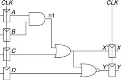
Figure 3.42 Sample circuit for timing analysis
Solution
Figure 3.43(a) shows waveforms illustrating when the signals might change. The inputs, A to D, are registered, so they only change shortly after CLK rises.
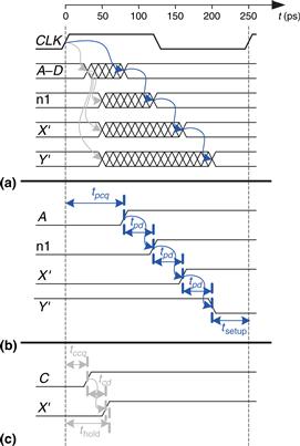
Figure 3.43 Timing diagram: (a) general case, (b) critical path, (c) short path
The critical path occurs when B = 1, C = 0, D = 0, and A rises from 0 to 1, triggering n1 to rise, X′ to rise, and Y′ to fall, as shown in Figure 3.43(b). This path involves three gate delays. For the critical path, we assume that each gate requires its full propagation delay. Y′ must setup before the next rising edge of the CLK. Hence, the minimum cycle time is
![]() (3.18)
(3.18)
The maximum clock frequency is fc = 1/Tc = 4 GHz.
A short path occurs when A = 0 and C rises, causing X′ to rise, as shown in Figure 3.43(c). For the short path, we assume that each gate switches after only a contamination delay. This path involves only one gate delay, so it may occur after tccq + tcd = 30 + 25 = 55 ps. But recall that the flip-flop has a hold time of 60 ps, meaning that X′ must remain stable for 60 ps after the rising edge of CLK for the flip-flop to reliably sample its value. In this case, X′ = 0 at the first rising edge of CLK, so we want the flip-flop to capture X = 0. Because X′ did not hold stable long enough, the actual value of X is unpredictable. The circuit has a hold time violation and may behave erratically at any clock frequency.
Example 3.11 Fixing Hold Time Violations
Alyssa P. Hacker proposes to fix Ben’s circuit by adding buffers to slow down the short paths, as shown in Figure 3.44. The buffers have the same delays as other gates. Determine the maximum clock frequency and whether any hold time problems could occur.
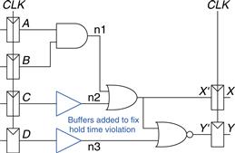
Figure 3.44 Corrected circuit to fix hold time problem
Solution
Figure 3.45 shows waveforms illustrating when the signals might change. The critical path from A to Y is unaffected, because it does not pass through any buffers. Therefore, the maximum clock frequency is still 4 GHz. However, the short paths are slowed by the contamination delay of the buffer. Now X′ will not change until tccq + 2tcd = 30 + 2 × 25 = 80 ps. This is after the 60 ps hold time has elapsed, so the circuit now operates correctly.

Figure 3.45 Timing diagram with buffers to fix hold time problem
This example had an unusually long hold time to illustrate the point of hold time problems. Most flip-flops are designed with thold < tccq to avoid such problems. However, some high-performance microprocessors, including the Pentium 4, use an element called a pulsed latch in place of a flip-flop. The pulsed latch behaves like a flip-flop but has a short clock-to-Q delay and a long hold time. In general, adding buffers can usually, but not always, solve hold time problems without slowing the critical path.
3.5.3 Clock Skew*
In the previous analysis, we assumed that the clock reaches all registers at exactly the same time. In reality, there is some variation in this time. This variation in clock edges is called clock skew. For example, the wires from the clock source to different registers may be of different lengths, resulting in slightly different delays, as shown in Figure 3.46. Noise also results in different delays. Clock gating, described in Section 3.2.5, further delays the clock. If some clocks are gated and others are not, there will be substantial skew between the gated and ungated clocks. In Figure 3.46, CLK2 is early with respect to CLK1, because the clock wire between the two registers follows a scenic route. If the clock had been routed differently, CLK1 might have been early instead. When doing timing analysis, we consider the worst-case scenario, so that we can guarantee that the circuit will work under all circumstances.
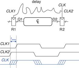
Figure 3.46 Clock skew caused by wire delay
Figure 3.47 adds skew to the timing diagram from Figure 3.38. The heavy clock line indicates the latest time at which the clock signal might reach any register; the hashed lines show that the clock might arrive up to tskew earlier.
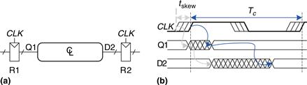
Figure 3.47 Timing diagram with clock skew
First, consider the setup time constraint shown in Figure 3.48. In the worst case, R1 receives the latest skewed clock and R2 receives the earliest skewed clock, leaving as little time as possible for data to propagate between the registers.
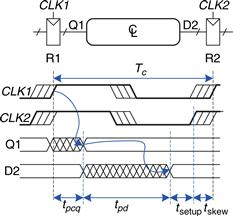
Figure 3.48 Setup time constraint with clock skew
The data propagates through the register and combinational logic and must setup before R2 samples it. Hence, we conclude that
![]() (3.19)
(3.19)
![]() (3.20)
(3.20)
Next, consider the hold time constraint shown in Figure 3.49. In the worst case, R1 receives an early skewed clock, CLK1, and R2 receives a late skewed clock, CLK2. The data zips through the register and combinational logic but must not arrive until a hold time after the late clock. Thus, we find that
![]() (3.21)
(3.21)
![]() (3.22)
(3.22)

Figure 3.49 Hold time constraint with clock skew
In summary, clock skew effectively increases both the setup time and the hold time. It adds to the sequencing overhead, reducing the time available for useful work in the combinational logic. It also increases the required minimum delay through the combinational logic. Even if thold = 0, a pair of back-to-back flip-flops will violate Equation 3.22 if tskew > tccq. To prevent serious hold time failures, designers must not permit too much clock skew. Sometimes flip-flops are intentionally designed to be particularly slow (i.e., large tccq), to prevent hold time problems even when the clock skew is substantial.
Example 3.12 Timing Analysis with Clock Skew
Revisit Example 3.10 and assume that the system has 50 ps of clock skew.
Solution
The critical path remains the same, but the setup time is effectively increased by the skew. Hence, the minimum cycle time is
![]() (3.23)
(3.23)
The maximum clock frequency is fc = 1/Tc = 3.33 GHz.
The short path also remains the same at 55 ps. The hold time is effectively increased by the skew to 60 + 50 = 110 ps, which is much greater than 55 ps. Hence, the circuit will violate the hold time and malfunction at any frequency. The circuit violated the hold time constraint even without skew. Skew in the system just makes the violation worse.
Example 3.13 Fixing Hold Time Violations
Revisit Example 3.11 and assume that the system has 50 ps of clock skew.
Solution
The critical path is unaffected, so the maximum clock frequency remains 3.33 GHz.
The short path increases to 80 ps. This is still less than thold + tskew = 110 ps, so the circuit still violates its hold time constraint.
To fix the problem, even more buffers could be inserted. Buffers would need to be added on the critical path as well, reducing the clock frequency. Alternatively, a better flip-flop with a shorter hold time might be used.
3.5.4 Metastability
As noted earlier, it is not always possible to guarantee that the input to a sequential circuit is stable during the aperture time, especially when the input arrives from the external world. Consider a button connected to the input of a flip-flop, as shown in Figure 3.50. When the button is not pressed, D = 0. When the button is pressed, D = 1. A monkey presses the button at some random time relative to the rising edge of CLK. We want to know the output Q after the rising edge of CLK. In Case I, when the button is pressed much before CLK, Q = 1. In Case II, when the button is not pressed until long after CLK, Q = 0. But in Case III, when the button is pressed sometime between tsetup before CLK and thold after CLK, the input violates the dynamic discipline and the output is undefined.
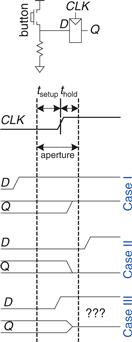
Figure 3.50 Input changing before, after, or during aperture
Metastable State
When a flip-flop samples an input that is changing during its aperture, the output Q may momentarily take on a voltage between 0 and VDD that is in the forbidden zone. This is called a metastable state. Eventually, the flip-flop will resolve the output to a stable state of either 0 or 1. However, the resolution time required to reach the stable state is unbounded.

The metastable state of a flip-flop is analogous to a ball on the summit of a hill between two valleys, as shown in Figure 3.51. The two valleys are stable states, because a ball in the valley will remain there as long as it is not disturbed. The top of the hill is called metastable because the ball would remain there if it were perfectly balanced. But because nothing is perfect, the ball will eventually roll to one side or the other. The time required for this change to occur depends on how nearly well balanced the ball originally was. Every bistable device has a metastable state between the two stable states.
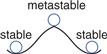
Figure 3.51 Stable and metastable states
Resolution Time
If a flip-flop input changes at a random time during the clock cycle, the resolution time, tres, required to resolve to a stable state is also a random variable. If the input changes outside the aperture, then tres = tpcq. But if the input happens to change within the aperture, tres can be substantially longer. Theoretical and experimental analyses (see Section 3.5.6) have shown that the probability that the resolution time, tres, exceeds some arbitrary time, t, decreases exponentially with t:
![]() (3.24)
(3.24)
where Tc is the clock period, and T0 and τ are characteristic of the flip-flop. The equation is valid only for t substantially longer than tpcq.
Intuitively, T0/Tc describes the probability that the input changes at a bad time (i.e., during the aperture time); this probability decreases with the cycle time, Tc. τ is a time constant indicating how fast the flip-flop moves away from the metastable state; it is related to the delay through the cross-coupled gates in the flip-flop.
In summary, if the input to a bistable device such as a flip-flop changes during the aperture time, the output may take on a metastable value for some time before resolving to a stable 0 or 1. The amount of time required to resolve is unbounded, because for any finite time, t, the probability that the flip-flop is still metastable is nonzero. However, this probability drops off exponentially as t increases. Therefore, if we wait long enough, much longer than tpcq, we can expect with exceedingly high probability that the flip-flop will reach a valid logic level.
3.5.5 Synchronizers
Asynchronous inputs to digital systems from the real world are inevitable. Human input is asynchronous, for example. If handled carelessly, these asynchronous inputs can lead to metastable voltages within the system, causing erratic system failures that are extremely difficult to track down and correct. The goal of a digital system designer should be to ensure that, given asynchronous inputs, the probability of encountering a metastable voltage is sufficiently small. “Sufficiently” depends on the context. For a cell phone, perhaps one failure in 10 years is acceptable, because the user can always turn the phone off and back on if it locks up. For a medical device, one failure in the expected life of the universe (1010 years) is a better target. To guarantee good logic levels, all asynchronous inputs should be passed through synchronizers.
A synchronizer, shown in Figure 3.52, is a device that receives an asynchronous input D and a clock CLK. It produces an output Q within a bounded amount of time; the output has a valid logic level with extremely high probability. If D is stable during the aperture, Q should take on the same value as D. If D changes during the aperture, Q may take on either a HIGH or LOW value but must not be metastable.

Figure 3.52 Synchronizer symbol
Figure 3.53 shows a simple way to build a synchronizer out of two flip-flops. F1 samples D on the rising edge of CLK. If D is changing at that time, the output D2 may be momentarily metastable. If the clock period is long enough, D2 will, with high probability, resolve to a valid logic level before the end of the period. F2 then samples D2, which is now stable, producing a good output Q.
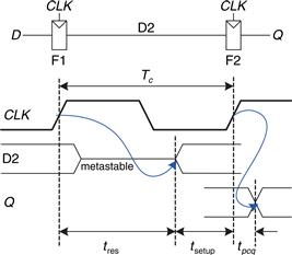
Figure 3.53 Simple synchronizer
We say that a synchronizer fails if Q, the output of the synchronizer, becomes metastable. This may happen if D2 has not resolved to a valid level by the time it must setup at F2—that is, if tres > Tc − tsetup. According to Equation 3.24, the probability of failure for a single input change at a random time is
![]() (3.25)
(3.25)
The probability of failure, P(failure), is the probability that the output Q will be metastable upon a single change in D. If D changes once per second, the probability of failure per second is just P(failure). However, if D changes N times per second, the probability of failure per second is N times as great:
![]() (3.26)
(3.26)
System reliability is usually measured in mean time between failures (MTBF). As the name suggests, MTBF is the average amount of time between failures of the system. It is the reciprocal of the probability that the system will fail in any given second
![]() (3.27)
(3.27)
Equation 3.27 shows that the MTBF improves exponentially as the synchronizer waits for a longer time, Tc. For most systems, a synchronizer that waits for one clock cycle provides a safe MTBF. In exceptionally high-speed systems, waiting for more cycles may be necessary.
Example 3.14 Synchronizer for FSM Input
The traffic light controller FSM from Section 3.4.1 receives asynchronous inputs from the traffic sensors. Suppose that a synchronizer is used to guarantee stable inputs to the controller. Traffic arrives on average 0.2 times per second. The flip-flops in the synchronizer have the following characteristics: τ = 200 ps, T0 = 150 ps, and tsetup = 500 ps. How long must the synchronizer clock period be for the MTBF to exceed 1 year?
Solution
1 year ≈ π × 107 seconds. Solve Equation 3.27.
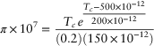 (3.28)
This equation has no closed form solution. However, it is easy enough to solve by guess and check. In a spreadsheet, try a few values of Tc and calculate the MTBF until discovering the value of Tc that gives an MTBF of 1 year: Tc = 3.036 ns.
3.5.6 Derivation of Resolution Time*
Equation 3.24 can be derived using a basic knowledge of circuit theory, differential equations, and probability. This section can be skipped if you are not interested in the derivation or if you are unfamiliar with the mathematics.
A flip-flop output will be metastable after some time, t, if the flip-flop samples a changing input (causing a metastable condition) and the output does not resolve to a valid level within that time after the clock edge. Symbolically, this can be expressed as
![]() (3.29)
(3.29)
We consider each probability term individually. The asynchronous input signal switches between 0 and 1 in some time, tswitch, as shown in Figure 3.54. The probability that the input changes during the aperture around the clock edge is
![]() (3.30)
(3.30)

Figure 3.54 Input timing
If the flip-flop does enter metastability—that is, with probability P(samples changing input)—the time to resolve from metastability depends on the inner workings of the circuit. This resolution time determines P(unresolved), the probability that the flip-flop has not yet resolved to a valid logic level after a time t. The remainder of this section analyzes a simple model of a bistable device to estimate this probability.
A bistable device uses storage with positive feedback. Figure 3.55(a) shows this feedback implemented with a pair of inverters; this circuit’s behavior is representative of most bistable elements. A pair of inverters behaves like a buffer. Let us model it as having the symmetric DC transfer characteristics shown in Figure 3.55(b), with a slope of G. The buffer can deliver only a finite amount of output current; we can model this as an output resistance, R. All real circuits also have some capacitance C that must be charged up. Charging the capacitor through the resistor causes an RC delay, preventing the buffer from switching instantaneously. Hence, the complete circuit model is shown in Figure 3.55(c), where vout(t) is the voltage of interest conveying the state of the bistable device.
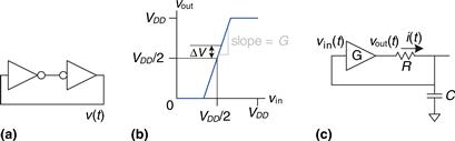
Figure 3.55 Circuit model of bistable device
The metastable point for this circuit is vout(t) = vin(t) = VDD/2; if the circuit began at exactly that point, it would remain there indefinitely in the absence of noise. Because voltages are continuous variables, the chance that the circuit will begin at exactly the metastable point is vanishingly small. However, the circuit might begin at time 0 near metastability at vout(0) = VDD/2 + ΔV for some small offset ΔV. In such a case, the positive feedback will eventually drive vout(t) to VDD if ΔV > 0 and to 0 if ΔV < 0. The time required to reach VDD or 0 is the resolution time of the bistable device.
The DC transfer characteristic is nonlinear, but it appears linear near the metastable point, which is the region of interest to us. Specifically, if vin(t) = VDD/2 + ΔV/G, then vout(t) = VDD/2 + ΔV for small ΔV. The current through the resistor is i(t) = (vout(t) − vin(t))/R. The capacitor charges at a rate dvin(t)/dt = i(t)/C. Putting these facts together, we find the governing equation for the output voltage.
![]() (3.31)
(3.31)
This is a linear first-order differential equation. Solving it with the initial condition vout(0) = VDD/2 + ΔV gives
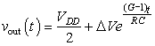 (3.32)
Figure 3.56 plots trajectories for vout(t) given various starting points. vout(t) moves exponentially away from the metastable point VDD/2 until it saturates at VDD or 0. The output eventually resolves to 1 or 0. The amount of time this takes depends on the initial voltage offset (ΔV) from the metastable point (VDD/2).

Figure 3.56 Resolution trajectories
Solving Equation 3.32 for the resolution time tres, such that vout(tres) = VDD or 0, gives
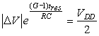 (3.33)
![]() (3.34)
(3.34)
In summary, the resolution time increases if the bistable device has high resistance or capacitance that causes the output to change slowly. It decreases if the bistable device has high gain, G. The resolution time also increases logarithmically as the circuit starts closer to the metastable point (ΔV → 0).
Define τ as ![]() . Solving Equation 3.34 for ΔV finds the initial offset, ΔVres, that gives a particular resolution time, tres:
. Solving Equation 3.34 for ΔV finds the initial offset, ΔVres, that gives a particular resolution time, tres:
![]() (3.35)
(3.35)
Suppose that the bistable device samples the input while it is changing. It measures a voltage, vin(0), which we will assume is uniformly distributed between 0 and VDD. The probability that the output has not resolved to a legal value after time tres depends on the probability that the initial offset is sufficiently small. Specifically, the initial offset on vout must be less than ΔVres, so the initial offset on vin must be less than ΔVres/G. Then the probability that the bistable device samples the input at a time to obtain a sufficiently small initial offset is
![]() (3.36)
(3.36)
Putting this all together, the probability that the resolution time exceeds some time t is given by the following equation:
![]() (3.37)
(3.37)
Observe that Equation 3.37 is in the form of Equation 3.24, where T0 = (tswitch + tsetup + thold)/G and τ = RC/(G − 1). In summary, we have derived Equation 3.24 and shown how T0 and τ depend on physical properties of the bistable device.
3.6 Parallelism
The speed of a system is characterized by the latency and throughput of information moving through it. We define a token to be a group of inputs that are processed to produce a group of outputs. The term conjures up the notion of placing subway tokens on a circuit diagram and moving them around to visualize data moving through the circuit. The latency of a system is the time required for one token to pass through the system from start to end. The throughput is the number of tokens that can be produced per unit time.

Example 3.15 Cookie Throughput and Latency
Ben Bitdiddle is throwing a milk and cookies party to celebrate the installation of his traffic light controller. It takes him 5 minutes to roll cookies and place them on his tray. It then takes 15 minutes for the cookies to bake in the oven. Once the cookies are baked, he starts another tray. What is Ben’s throughput and latency for a tray of cookies?
Solution
In this example, a tray of cookies is a token. The latency is 1/3 hour per tray. The throughput is 3 trays/hour.
As you might imagine, the throughput can be improved by processing several tokens at the same time. This is called parallelism, and it comes in two forms: spatial and temporal. With spatial parallelism, multiple copies of the hardware are provided so that multiple tasks can be done at the same time. With temporal parallelism, a task is broken into stages, like an assembly line. Multiple tasks can be spread across the stages. Although each task must pass through all stages, a different task will be in each stage at any given time so multiple tasks can overlap. Temporal parallelism is commonly called pipelining. Spatial parallelism is sometimes just called parallelism, but we will avoid that naming convention because it is ambiguous.
Example 3.16 Cookie Parallelism
Ben Bitdiddle has hundreds of friends coming to his party and needs to bake cookies faster. He is considering using spatial and/or temporal parallelism.
Spatial Parallelism: Ben asks Alyssa P. Hacker to help out. She has her own cookie tray and oven.
Temporal Parallelism: Ben gets a second cookie tray. Once he puts one cookie tray in the oven, he starts rolling cookies on the other tray rather than waiting for the first tray to bake.
What is the throughput and latency using spatial parallelism? Using temporal parallelism? Using both?
Solution
The latency is the time required to complete one task from start to finish. In all cases, the latency is 1/3 hour. If Ben starts with no cookies, the latency is the time needed for him to produce the first cookie tray.
The throughput is the number of cookie trays per hour. With spatial parallelism, Ben and Alyssa each complete one tray every 20 minutes. Hence, the throughput doubles, to 6 trays/hour. With temporal parallelism, Ben puts a new tray in the oven every 15 minutes, for a throughput of 4 trays/hour. These are illustrated in Figure 3.57.
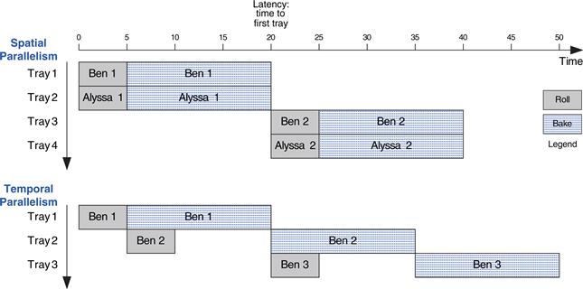
Figure 3.57 Spatial and temporal parallelism in the cookie kitchen
If Ben and Alyssa use both techniques, they can bake 8 trays/hour.
Consider a task with latency L. In a system with no parallelism, the throughput is 1/L. In a spatially parallel system with N copies of the hardware, the throughput is N/L. In a temporally parallel system, the task is ideally broken into N steps, or stages, of equal length. In such a case, the throughput is also N/L, and only one copy of the hardware is required. However, as the cookie example showed, finding N steps of equal length is often impractical. If the longest step has a latency L1, the pipelined throughput is 1/L1.
Pipelining (temporal parallelism) is particularly attractive because it speeds up a circuit without duplicating the hardware. Instead, registers are placed between blocks of combinational logic to divide the logic into shorter stages that can run with a faster clock. The registers prevent a token in one pipeline stage from catching up with and corrupting the token in the next stage.
Figure 3.58 shows an example of a circuit with no pipelining. It contains four blocks of logic between the registers. The critical path passes through blocks 2, 3, and 4. Assume that the register has a clock-to-Q propagation delay of 0.3 ns and a setup time of 0.2 ns. Then the cycle time is Tc = 0.3 + 3 + 2 + 4 + 0.2 = 9.5 ns. The circuit has a latency of 9.5 ns and a throughput of 1/9.5 ns = 105 MHz.

Figure 3.58 Circuit with no pipelining
Figure 3.59 shows the same circuit partitioned into a two-stage pipeline by adding a register between blocks 3 and 4. The first stage has a minimum clock period of 0.3 + 3 + 2 + 0.2 = 5.5 ns. The second stage has a minimum clock period of 0.3 + 4 + 0.2 = 4.5 ns. The clock must be slow enough for all stages to work. Hence, Tc = 5.5 ns. The latency is two clock cycles, or 11 ns. The throughput is 1/5.5 ns = 182 MHz. This example shows that, in a real circuit, pipelining with two stages almost doubles the throughput and slightly increases the latency. In comparison, ideal pipelining would exactly double the throughput at no penalty in latency. The discrepancy comes about because the circuit cannot be divided into two exactly equal halves and because the registers introduce more sequencing overhead.
Figure 3.59 Circuit with two-stage pipeline
Figure 3.60 shows the same circuit partitioned into a three-stage pipeline. Note that two more registers are needed to store the results of blocks 1 and 2 at the end of the first pipeline stage. The cycle time is now limited by the third stage to 4.5 ns. The latency is three cycles, or 13.5 ns. The throughput is 1/4.5 ns = 222 MHz. Again, adding a pipeline stage improves throughput at the expense of some latency.
Figure 3.60 Circuit with three-stage pipeline
Although these techniques are powerful, they do not apply to all situations. The bane of parallelism is dependencies. If a current task is dependent on the result of a prior task, rather than just prior steps in the current task, the task cannot start until the prior task has completed. For example, if Ben wants to check that the first tray of cookies tastes good before he starts preparing the second, he has a dependency that prevents pipelining or parallel operation. Parallelism is one of the most important techniques for designing high-performance digital systems. Chapter 7 discusses pipelining further and shows examples of handling dependencies.
3.7 Summary
This chapter has described the analysis and design of sequential logic. In contrast to combinational logic, whose outputs depend only on the current inputs, sequential logic outputs depend on both current and prior inputs. In other words, sequential logic remembers information about prior inputs. This memory is called the state of the logic.
Anyone who could invent logic whose outputs depend on future inputs would be fabulously wealthy!
Sequential circuits can be difficult to analyze and are easy to design incorrectly, so we limit ourselves to a small set of carefully designed building blocks. The most important element for our purposes is the flip-flop, which receives a clock and an input D and produces an output Q. The flip-flop copies D to Q on the rising edge of the clock and otherwise remembers the old state of Q. A group of flip-flops sharing a common clock is called a register. Flip-flops may also receive reset or enable control signals.
Although many forms of sequential logic exist, we discipline ourselves to use synchronous sequential circuits because they are easy to design. Synchronous sequential circuits consist of blocks of combinational logic separated by clocked registers. The state of the circuit is stored in the registers and updated only on clock edges.
Finite state machines are a powerful technique for designing sequential circuits. To design an FSM, first identify the inputs and outputs of the machine and sketch a state transition diagram, indicating the states and the transitions between them. Select an encoding for the states, and rewrite the diagram as a state transition table and output table, indicating the next state and output given the current state and input. From these tables, design the combinational logic to compute the next state and output, and sketch the circuit.
Synchronous sequential circuits have a timing specification including the clock-to-Q propagation and contamination delays, tpcq and tccq, and the setup and hold times, tsetup and thold. For correct operation, their inputs must be stable during an aperture time that starts a setup time before the rising edge of the clock and ends a hold time after the rising edge of the clock. The minimum cycle time Tc of the system is equal to the propagation delay tpd through the combinational logic plus tpcq + tsetup of the register. For correct operation, the contamination delay through the register and combinational logic must be greater than thold. Despite the common misconception to the contrary, hold time does not affect the cycle time.
Overall system performance is measured in latency and throughput. The latency is the time required for a token to pass from start to end. The throughput is the number of tokens that the system can process per unit time. Parallelism improves system throughput.
Exercises
Exercise 3.1 Given the input waveforms shown in Figure 3.61, sketch the output, Q, of an SR latch.

Figure 3.61 Input waveforms of SR latch for Exercise 3.1
Exercise 3.2 Given the input waveforms shown in Figure 3.62, sketch the output, Q, of an SR latch.

Figure 3.62 Input waveforms of SR latch for Exercise 3.2
Exercise 3.3 Given the input waveforms shown in Figure 3.63, sketch the output, Q, of a D latch.
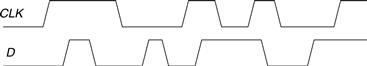
Figure 3.63 Input waveforms of D latch or flip-flop for Exercises 3.3 and 3.5
Exercise 3.4 Given the input waveforms shown in Figure 3.64, sketch the output, Q, of a D latch.

Figure 3.64 Input waveforms of D latch or flip-flop for Exercises 3.4 and 3.6
Exercise 3.5 Given the input waveforms shown in Figure 3.63, sketch the output, Q, of a D flip-flop.
Exercise 3.6 Given the input waveforms shown in Figure 3.64, sketch the output, Q, of a D flip-flop.
Exercise 3.7 Is the circuit in Figure 3.65 combinational logic or sequential logic? Explain in a simple fashion what the relationship is between the inputs and outputs. What would you call this circuit?
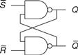
Figure 3.65 Mystery circuit
Exercise 3.8 Is the circuit in Figure 3.66 combinational logic or sequential logic? Explain in a simple fashion what the relationship is between the inputs and outputs. What would you call this circuit?
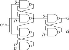
Figure 3.66 Mystery circuit
Exercise 3.9 The toggle (T) flip-flop has one input, CLK, and one output, Q. On each rising edge of CLK, Q toggles to the complement of its previous value. Draw a schematic for a T flip-flop using a D flip-flop and an inverter.
Exercise 3.10 A JK flip-flop receives a clock and two inputs, J and K. On the rising edge of the clock, it updates the output, Q. If J and K are both 0, Q retains its old value. If only J is 1, Q becomes 1. If only K is 1, Q becomes 0. If both J and K are 1, Q becomes the opposite of its present state.
(a) Construct a JK flip-flop using a D flip-flop and some combinational logic.
(b) Construct a D flip-flop using a JK flip-flop and some combinational logic.
(c) Construct a T flip-flop (see Exercise 3.9) using a JK flip-flop.
Exercise 3.11 The circuit in Figure 3.67 is called a Muller C-element. Explain in a simple fashion what the relationship is between the inputs and output.
Figure 3.67 Muller C-element
Exercise 3.12 Design an asynchronously resettable D latch using logic gates.
Exercise 3.13 Design an asynchronously resettable D flip-flop using logic gates.
Exercise 3.14 Design a synchronously settable D flip-flop using logic gates.
Exercise 3.15 Design an asynchronously settable D flip-flop using logic gates.
Exercise 3.16 Suppose a ring oscillator is built from N inverters connected in a loop. Each inverter has a minimum delay of tcd and a maximum delay of tpd. If N is odd, determine the range of frequencies at which the oscillator might operate.
Exercise 3.17 Why must N be odd in Exercise 3.16?
Exercise 3.18 Which of the circuits in Figure 3.68 are synchronous sequential circuits? Explain.
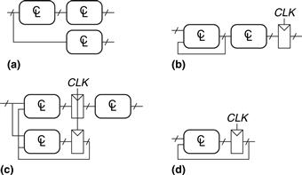
Figure 3.68 Circuits
Exercise 3.19 You are designing an elevator controller for a building with 25 floors. The controller has two inputs: UP and DOWN. It produces an output indicating the floor that the elevator is on. There is no floor 13. What is the minimum number of bits of state in the controller?
Exercise 3.20 You are designing an FSM to keep track of the mood of four students working in the digital design lab. Each student’s mood is either HAPPY (the circuit works), SAD (the circuit blew up), BUSY (working on the circuit), CLUELESS (confused about the circuit), or ASLEEP (face down on the circuit board). How many states does the FSM have? What is the minimum number of bits necessary to represent these states?
Exercise 3.21 How would you factor the FSM from Exercise 3.20 into multiple simpler machines? How many states does each simpler machine have? What is the minimum total number of bits necessary in this factored design?
Exercise 3.22 Describe in words what the state machine in Figure 3.69 does. Using binary state encodings, complete a state transition table and output table for the FSM. Write Boolean equations for the next state and output and sketch a schematic of the FSM.

Figure 3.69 State transition diagram
Exercise 3.23 Describe in words what the state machine in Figure 3.70 does. Using binary state encodings, complete a state transition table and output table for the FSM. Write Boolean equations for the next state and output and sketch a schematic of the FSM.
Figure 3.70 State transition diagram
Exercise 3.24 Accidents are still occurring at the intersection of Academic Avenue and Bravado Boulevard. The football team is rushing into the intersection the moment light B turns green. They are colliding with sleep-deprived CS majors who stagger into the intersection just before light A turns red. Extend the traffic light controller from Section 3.4.1 so that both lights are red for 5 seconds before either light turns green again. Sketch your improved Moore machine state transition diagram, state encodings, state transition table, output table, next state and output equations, and your FSM schematic.
Exercise 3.25 Alyssa P. Hacker’s snail from Section 3.4.3 has a daughter with a Mealy machine FSM brain. The daughter snail smiles whenever she slides over the pattern 1101 or the pattern 1110. Sketch the state transition diagram for this happy snail using as few states as possible. Choose state encodings and write a combined state transition and output table using your encodings. Write the next state and output equations and sketch your FSM schematic.
Exercise 3.26 You have been enlisted to design a soda machine dispenser for your department lounge. Sodas are partially subsidized by the student chapter of the IEEE, so they cost only 25 cents. The machine accepts nickels, dimes, and quarters. When enough coins have been inserted, it dispenses the soda and returns any necessary change. Design an FSM controller for the soda machine. The FSM inputs are Nickel, Dime, and Quarter, indicating which coin was inserted. Assume that exactly one coin is inserted on each cycle. The outputs are Dispense, ReturnNickel, ReturnDime, and ReturnTwoDimes. When the FSM reaches 25 cents, it asserts Dispense and the necessary Return outputs required to deliver the appropriate change. Then it should be ready to start accepting coins for another soda.
Exercise 3.27 Gray codes have a useful property in that consecutive numbers differ in only a single bit position. Table 3.23 lists a 3-bit Gray code representing the numbers 0 to 7. Design a 3-bit modulo 8 Gray code counter FSM with no inputs and three outputs. (A modulo N counter counts from 0 to N − 1, then repeats. For example, a watch uses a modulo 60 counter for the minutes and seconds that counts from 0 to 59.) When reset, the output should be 000. On each clock edge, the output should advance to the next Gray code. After reaching 100, it should repeat with 000.
Table 3.23 3-bit Gray code
Exercise 3.28 Extend your modulo 8 Gray code counter from Exercise 3.27 to be an UP/DOWN counter by adding an UP input. If UP = 1, the counter advances to the next number. If UP = 0, the counter retreats to the previous number.
Exercise 3.29 Your company, Detect-o-rama, would like to design an FSM that takes two inputs, A and B, and generates one output, Z. The output in cycle n, Zn, is either the Boolean AND or OR of the corresponding input An and the previous input An-1, depending on the other input, Bn:
![]()
(a) Sketch the waveform for Z given the inputs shown in Figure 3.71.
Figure 3.71 FSM input waveforms
(b) Is this FSM a Moore or a Mealy machine?
(c) Design the FSM. Show your state transition diagram, encoded state transition table, next state and output equations, and schematic.
Exercise 3.30 Design an FSM with one input, A, and two outputs, X and Y. X should be 1 if A has been 1 for at least three cycles altogether (not necessarily consecutively). Y should be 1 if A has been 1 for at least two consecutive cycles. Show your state transition diagram, encoded state transition table, next state and output equations, and schematic.
Exercise 3.31 Analyze the FSM shown in Figure 3.72. Write the state transition and output tables and sketch the state transition diagram. Describe in words what the FSM does.

Figure 3.72 FSM schematic
Exercise 3.32 Repeat Exercise 3.31 for the FSM shown in Figure 3.73. Recall that the s and r register inputs indicate set and reset, respectively.
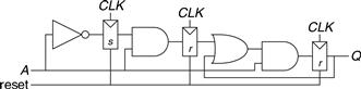
Figure 3.73 FSM schematic
Exercise 3.33 Ben Bitdiddle has designed the circuit in Figure 3.74 to compute a registered four-input XOR function. Each two-input XOR gate has a propagation delay of 100 ps and a contamination delay of 55 ps. Each flip-flop has a setup time of 60 ps, a hold time of 20 ps, a clock-to-Q maximum delay of 70 ps, and a clock-to-Q minimum delay of 50 ps.
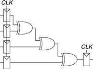
Figure 3.74 Registered four-input XOR circuit
(a) If there is no clock skew, what is the maximum operating frequency of the circuit?
(b) How much clock skew can the circuit tolerate if it must operate at 2 GHz?
(c) How much clock skew can the circuit tolerate before it might experience a hold time violation?
(d) Alyssa P. Hacker points out that she can redesign the combinational logic between the registers to be faster and tolerate more clock skew. Her improved circuit also uses three two-input XORs, but they are arranged differently. What is her circuit? What is its maximum frequency if there is no clock skew? How much clock skew can the circuit tolerate before it might experience a hold time violation?
Exercise 3.34 You are designing an adder for the blindingly fast 2-bit RePentium Processor. The adder is built from two full adders such that the carry out of the first adder is the carry in to the second adder, as shown in Figure 3.75. Your adder has input and output registers and must complete the addition in one clock cycle. Each full adder has the following propagation delays: 20 ps from Cin to Cout or to Sum (S), 25 ps from A or B to Cout, and 30 ps from A or B to S. The adder has a contamination delay of 15 ps from Cin to either output and 22 ps from A or B to either output. Each flip-flop has a setup time of 30 ps, a hold time of 10 ps, a clock-to-Q propagation delay of 35 ps, and a clock-to-Q contamination delay of 21 ps.

Figure 3.75 2-bit adder schematic
(a) If there is no clock skew, what is the maximum operating frequency of the circuit?
(b) How much clock skew can the circuit tolerate if it must operate at 8 GHz?
(c) How much clock skew can the circuit tolerate before it might experience a hold time violation?
Exercise 3.35 A field programmable gate array (FPGA) uses configurable logic blocks (CLBs) rather than logic gates to implement combinational logic. The Xilinx Spartan 3 FPGA has propagation and contamination delays of 0.61 and 0.30 ns, respectively, for each CLB. It also contains flip-flops with propagation and contamination delays of 0.72 and 0.50 ns, and setup and hold times of 0.53 and 0 ns, respectively.
(a) If you are building a system that needs to run at 40 MHz, how many consecutive CLBs can you use between two flip-flops? Assume there is no clock skew and no delay through wires between CLBs.
(b) Suppose that all paths between flip-flops pass through at least one CLB. How much clock skew can the FPGA have without violating the hold time?
Exercise 3.36 A synchronizer is built from a pair of flip-flops with tsetup = 50 ps, T0 = 20 ps, and τ = 30 ps. It samples an asynchronous input that changes 108 times per second. What is the minimum clock period of the synchronizer to achieve a mean time between failures (MTBF) of 100 years?
Exercise 3.37 You would like to build a synchronizer that can receive asynchronous inputs with an MTBF of 50 years. Your system is running at 1 GHz, and you use sampling flip-flops with τ = 100 ps, T0 = 110 ps, and tsetup = 70 ps. The synchronizer receives a new asynchronous input on average 0.5 times per second (i.e., once every 2 seconds). What is the required probability of failure to satisfy this MTBF? How many clock cycles would you have to wait before reading the sampled input signal to give that probability of error?
Exercise 3.38 You are walking down the hallway when you run into your lab partner walking in the other direction. The two of you first step one way and are still in each other’s way. Then you both step the other way and are still in each other’s way. Then you both wait a bit, hoping the other person will step aside. You can model this situation as a metastable point and apply the same theory that has been applied to synchronizers and flip-flops. Suppose you create a mathematical model for yourself and your lab partner. You start the unfortunate encounter in the metastable state. The probability that you remain in this state after t seconds is ![]() τ indicates your response rate; today, your brain has been blurred by lack of sleep and has τ = 20 seconds.
τ indicates your response rate; today, your brain has been blurred by lack of sleep and has τ = 20 seconds.
(a) How long will it be until you have 99% certainty that you will have resolved from metastability (i.e., figured out how to pass one another)?
(b) You are not only sleepy, but also ravenously hungry. In fact, you will starve to death if you don’t get going to the cafeteria within 3 minutes. What is the probability that your lab partner will have to drag you to the morgue?
Exercise 3.39 You have built a synchronizer using flip-flops with T0 = 20 ps and τ = 30 ps. Your boss tells you that you need to increase the MTBF by a factor of 10. By how much do you need to increase the clock period?
Exercise 3.40 Ben Bitdiddle invents a new and improved synchronizer in Figure 3.76 that he claims eliminates metastability in a single cycle. He explains that the circuit in box M is an analog “metastability detector” that produces a HIGH output if the input voltage is in the forbidden zone between VIL and VIH. The metastability detector checks to determine whether the first flip-flop has produced a metastable output on D2. If so, it asynchronously resets the flip-flop to produce a good 0 at D2. The second flip-flop then samples D2, always producing a valid logic level on Q. Alyssa P. Hacker tells Ben that there must be a bug in the circuit, because eliminating metastability is just as impossible as building a perpetual motion machine. Who is right? Explain, showing Ben’s error or showing why Alyssa is wrong.

Figure 3.76 “New and improved” synchronizer
Interview Questions
The following exercises present questions that have been asked at interviews for digital design jobs.
Question 3.1 Draw a state machine that can detect when it has received the serial input sequence 01010.
Question 3.2 Design a serial (one bit at a time) two’s complementer FSM with two inputs, Start and A, and one output, Q. A binary number of arbitrary length is provided to input A, starting with the least significant bit. The corresponding bit of the output appears at Q on the same cycle. Start is asserted for one cycle to initialize the FSM before the least significant bit is provided.
Question 3.3 What is the difference between a latch and a flip-flop? Under what circumstances is each one preferable?
Question 3.4 Design a 5-bit counter finite state machine.
Question 3.5 Design an edge detector circuit. The output should go HIGH for one cycle after the input makes a 0 → 1 transition.
Question 3.6 Describe the concept of pipelining and why it is used.
Question 3.7 Describe what it means for a flip-flop to have a negative hold time.
Question 3.8 Given signal A, shown in Figure 3.77, design a circuit that produces signal B.
![]()
Figure 3.77 Signal waveforms
Question 3.9 Consider a block of logic between two registers. Explain the timing constraints. If you add a buffer on the clock input of the receiver (the second flip-flop), does the setup time constraint get better or worse?