
Chapter 4
Nanotechnology
Chapter Contents
4.1 Top-Down, Bottom-Up
4.1.1 Nanolithography
4.1.2 Introduction to the Need for New Lithographic Techniques
4.1.3 Nanolithographic Techniques
4.1.4 Top-Down Nanolithographic Principles
4.1.5 Nanolithographic Technologies for the Microelectronics Industry
Deep Ultraviolet (DUV) Lithography
Extreme Ultraviolet (EUV) Lithography
4.1.6 Nanoimprint Technology
4.1.7 Case Studies: Nanoimprint Applications
4.1.8 Emerging Nanolithographic Technologies
Multiple E-Beam/Ion-Beam Lithography
4.1.9 Nanolithography in R&D
DUV Interference Nanolithography
EUV Interference Nanolithography
4.1.10 LIL Development at MESA+ NanoLab NL
Multi-exposures and Novel Resist Systems for 266 nm LIL
4.1.11 Case Study: Laser Interference Lithography Nanoarrays for Cell Biology
4.1.12 Concluding Remarks on Emerging Nanolithography
4.2 Nanomaterials
4.2.1 Ordered Oxides
4.2.2 Oxide Nanoarrays: Definitions and Background
Natural versus Artificial Oxide Nanoarrays
Oxide Metamaterials: How Do They Differ from Nanoarrays?
Curiosity-Driven Research on Nanoscale Metamaterials
Application-Driven Research on Nanoscale Oxide Metamaterials
4.2.3 Principles of Oxide Nanoarray Fabrication
Lithographic-Assisted Oxide Nanoarrays
Bio-inspired and Biotemplated Oxide Nanoarrays
4.2.4 Ordered Oxides in Medical Applications
Novel Nanoarrays in Diagnostics
Perspectives on Nanoarray in Therapy
4.3 Where Are We?
4.4 Where to Go from Here?
At the same time as processes to shape matter at ever smaller scales, starting with the work piece (Chapters 2 and 3) were developing, another trend appeared. The first set of techniques and processes are referred to collectively as the top-down approach; the new trend considers manufacturing from the bottom-up, relying on processes known from materials sciences and chemical synthesis. This is not new – nature has become a strong source of inspiration for designers who follow the bottom-up approach in many fields. Process development in the engineering sciences has not only focused on copying from the large to the small, but has also borrowed design strategies from nature and made them into novel, artificially created functions. The latter is often called biomimetics or biomimickry, and has found its way into a range of applications, from self-healing materials in aircraft design to reconstructive medicine. Eventually, the combination of top-down and bottom-up techniques will allow for even more functionality to be combined within a single miniaturized device.
The basic principles of such advanced fabrication methods are the processes of self-assembly and replication. In this context, replication is often referred to as templating. Today, artificially produced devices that can interact intimately with natural body functions are regularly used to replace lost abilities, and have become fully accepted in society. Some examples are artificial limbs, artificial heart valves and vascular-type systems, stents, heart pace makers, cochlear implants, as well as other electrodes which interact with the brain or nervous system such as retina implants and muscle stimulators. At the interface between articifical and biological materials (e.g., implant surface) bionanotechnology gains a particular importance. As well as biomedical engineers, specialists in other fields benefit from these nanoscale developments, for example, in the microelectronics industry (polymer electronics, single-molecule transistor, etc.), or in the further development of novel, advanced microfabrication processes.
In general, better more cost-effective fabrication technology is one of the important drivers for innovation that will lead to an increasing number of novel industrial applications. It is important to stress that nanotechnology is not a single discipline but a field of technology facilitating either the controlled creation, the study of phenomena, or the manipulation of matter at nanoscale dimensions. The fact that highly ordered material systems can be created within a film or bulk structure at the nanoscale facilities often a novel working mechanism but it is the order maintained across multiple length scales that is directly related to control of a system’s functions. One can conclude that it is this advanced, man-made, control of functionality down to the nanoscale which characterizes the field of nanotechnology across all scientific disciplines.
A general overview of nanofabrication is given in the book Micro-Nanofabrication by Zheng Cui, which presents the principles, capabilities and limits of nanofabrication in the current context of microsystems technologies [1]. I have also written recent reviews on nanolithography for parallel fabrication of nanoarrays in general, and oxide nanoarrays in particular [2, 3]. The following sections will provide an introduction into the field of nanotechnology with specific reference to ordered systems (arrays) and then an overview for further reading on the topic.
4.1 Top-Down, Bottom-Up
Initially, there was only one philosophy: the philosophy of miniaturization. In engineering terms, this means that the individual building blocks of a system will become smaller and smaller in size, or will replaced by integrated components requiring less space, since assembly is now omitted. The layers deposited throughout a variety of processes are now definable atom-by-atom. This is a tremendous paradigm shift in microtechnology. Consequently, adding the entire field of materials engineering to microsystems technology demands a clarification of the terminology that is used in this field. Historically, electrical and mechanical engineering relied on top-down techniques, while materials and chemical engineering worked from the bottom-up and aimed at modifying a material’s properties. In real-world systems, experts from both fields combine their separate approaches, and nanotechnology could be considered as a meeting point, where the focus is on the definition of features and processes (e.g., electron transfer) at a scale of a few nanometers. Figure 4.1 illustrates these two opposite approaches to nanotechnology, top-down and bottom-up, with examples of their applications.
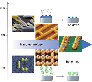
Figure 4.1 Top-down and bottom-up nanotechnology. In nanolithographic methods, generating structures at the nanoscale from the top-down maskless or through a mask, patterning can be achieved by writing or printing (from a mask or mold). When a mold is used for imprinting the technique is sometimes also called stamping. In nanotechnology from the bottom-up by self-organization of species, like molecules and solid-state architectures (nanocrystals, quantum dots) from the atomic to the mesoscopic scale, we can distinguish either pure self-assembly or combination thereof with a predefined template generated from the top-down. If such a combination is used we often also call these techniques nanolithography. Shown (clockwise from top) are: an electron microscopy image of a nanomechanical electrometer obtained by e-beam (top-down); patterned film of carbon nanotubes obtained by microcontact printing and catalytic growth (template-assisted bottom-up); a single carbon nanotube connecting two electrodes (electrodes by top-down, whereas positional assembly of the carbon nanotube onto the electrodes is performed manually utilizing the tip of a scanning probe); a regular metal–organic nanoporous network integration of iron atoms and functional molecules, where the iron atoms act as a template in the coordination of the molecules (self-organization from the bottom-up, sometimes also called coordination chemistry); and seven carbon monoxide molecules form the letter ‘C’ positioned with the tip of a scanning tunneling microscope.
Image originally taken from http://www.physics.ubc.ca/stm/, reprinted from [4] by permission from
4.1.1 Nanolithography
This section provides an overview of nanolithographic techniques, focusing on nanoarrays. Using patterning techniques such as lithography, we normally aim for a higher order architecture similar to functional systems in nature. Inspired by its wealth of complexity these architectures are translated into technical devices such as, for example, those found in integrated circuitry or other systems in which structural elements work as discrete building blocks in microdevices. Ordered artificial nanostructures (arrays of pillars, holes and wires) have shown particular properties, and bring about the opportunity to modify and tune the device operation. Moreover, these nanostructures open new applications, for example, the nanoscale control of spin direction within a nanomagnet. We can then look for applications where this unique property of the smallest manufactured element is repetitively used – with respect to spin, this would be in nanopatterned magnetic media for data storage.
These highly ordered, parallel manufactured nanostructures are generally called nanoarrays. Most of these applications require massively parallel produced nanopatterns which can be directly realized by laser interference (areas up to 4 cm2 are easily achieved with a Lloyd’s mirror set-up). In this overview we will further highlight the application of laser interference as a tool for nanofabrication, and its utilization as a primary patterning method for nanoimprint applications. Laser interference has great potential for producing simple (dots, lines, ellipses) and periodically repetitive patterns which could potentially be used in a range of devices, including nanostructuring for photonic crystal devices, high resolution patterned media, and surface modifications of medical implants. Laser interference lithography on the other hand clearly has limitations in terms of pattern freedom.
The unique properties of nanostructured surfaces have found applications in biomedical nanoarrays, either for diagnostic or functional assays, including catalytic reactions on chip. Bio-inspired, templated nanoarrays will be discussed in terms of how they fit with other massively parallel nanolithographic techniques currently under development in nanotechnological applications.
4.1.2 Introduction to the Need for New Lithographic Techniques
The vast amount of publications concerning lithographic techniques, which are capable of forming structures with lateral dimensions below 100 nm, suggest that high-end exposure techniques are well established. Particularly, in microelectronic systems, production machines are currently under development which are capable of reaching the 32 nm node, which is defined as the average half-pitch within a semiconductor pattern. Ultimate resolution, i.e., controlling functional elements at the molecule, atom, electron or spin scale, remains the major goal for further lithography research. This research field has consequently been branded nanolithography. A selection of nanolithographic techniques are of particular interest for their ability to produce massively parallel, repetitive nanostructures. Each technique needs to be evaluated on the basis of the following three criteria:
1. capability of the lithographic technique to resolve lateral features at a scale below 500 nm,
2. provision of an extremely high ordering across the desired manufacturing area, and
3. distinct positional control of placing, and ability to address an individual feature within the system.
A single feature reduced to the nanoscale (e.g., a dot) may by itself already possess remarkable properties, like unique electron transport properties, that are yet to be fully discovered [5]. Applications which make use of the repetitive nature of uniform nanostructures across a large manufacturing area have already demonstrated their potential, e.g., in patterned media (PM) for data storage [6].
This overview is a compilation of the literature which discussed major recent nanolithographic principles used in the pattern transfer of these massively parallel nanostructures. It is important to distinguish these nanoarrays with geometrical features at the nanoscale from biological screening arrays containing nanolitre-sized wells, which are also called nanoarrays [7].
Often the research on nanolithography for the fabrication of a nanoarray is dedicated to a specific application field, such as the fabrication of data storage media, photonic crystals and nanoarrays for diagnostics. For a better understanding of how these lithographic techniques may be characterized, Figure 4.2 shows the relation between the length scales of interest and their extreme demands on placement accuracy to achieve the required high ordering of the nanofeatures. Ideally, nanoarrays can be produced across the full area of an industrial scale wafer surface – generally a diameter of 6 inches or more, although for many devices such extreme large-area and continuous patterning may not be required. Considering that defect-free patterning across the area of a typical microelectronic silicon die of 26 × 33 mm2 is already a major challenge, we define here an area of 1 cm2 as large.
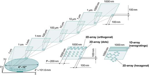
Figure 4.2 Definition of lithographically manufactured nanoarrays consisting nanofeatures at the scale of 100 nm.
Reproduced from reference [2] with permission from IOP Publishing.
Figure 4.3 presents two kinds of nanoarray layouts: the continuous and the discontinuous nanoarray, where the latter is defined by repetitive clusters of nanoscale features that in themselves are also ordered. Comparing nanoarrays to a continuous thin-film layer of the same material can deliver novel properties to the layer. One example of this is a photonic crystal. Such crystals have tunable optical properties for guiding light within them, in a way that is defined by the lateral feature size, shape and periodicity of the individual nanostructures. These nanostructured materials are often called metamaterials (see section 4.2).

Figure 4.3 Definition of (A) discontinuous and (B) continuous nanoarrays, and (C) possible errors. Both (A) and (B) can deliver metamaterial properties dependent on the combination of the dimension of the single feature and the meta-period (Pmeta) of its repetition within the array. A field is defined here by 1000 × 1000 nm2. Alignment errors, positioning from field to field (stitching), overlay errors and placement errors within one field can occur. These errors will depend on the lithographic technique and are not generally defined. A typical microelectronic chip (die) covers, e.g. an area of 26 × 33 mm2. In the semiconductor industry a roadmap is assembled to illustrate lithographic needs for innovation. A novel lithography technique must guarantee a certain degree of fault-free structuring within the patterning fields across the die. Of course, the exact definition of feature tolerances highly depends on the function of a device. For semiconductor devices a summary of these definitions can be found at [10].
Reproduced from reference [2] with permission from IOP Publishing.
Finally, we need to define the difference between the lithography and the pattern transfer step (see also Chapter 2). Generally, transfer means that a pattern is carried over from one layer to another. These layers are either chosen for their masking, functional, or sacrificial nature, such as for example a silicon nitride layer on silicon, where the nitride layer protects the silicon during etching.
Typically, lithography employs a resist layer. This layer is normally a polymer that is sensitive to light of a certain wavelength and etch-resistant in the transfer step – hence the name resist. Recently, a range of inorganic resists have been indentified, for example, sol-gel based resists in nanoimprint lithography [8]. The pattern is transferred from the mask to the resist by an exposure step, from a resist to an underlying functional layer by etching, or from a resist to an added layer by deposition and lift-off. Many varieties of process sequence for pattern transfer are known and several extensive texts are available, for example, Handbook of Microlithography, Micromachining and Microfabrication [9].
At a length scale below the lateral width of 500 nm, it becomes extremely difficult to fabricate structures from the top-down using 365 nm-ultraviolet (UV) photolithographic techniques through a mask, because of diffraction of the light at the mask openings. Moving to a shorter wavelength, specifically deep ultraviolet (DUV), is practicable, for the sub-500 nm domain, but few such industrial systems are accessible to researchers in the field of nanotechnology. Since these machines are dedicated to electronics, they will not be reviewed in detail here, but briefly discussed in the context of next generation nanolithography principles (section 4.1.3). Features can be made quite reliably, even down to a few nanometers, by electron-beam lithography, however. Current, state-of-the-art electron beam (e-beam) lithography is an indispensable technique for the fabrication of templates (also named masters or molds) for nanotechnological applications. This top-down technique is extremely slow and, as shown in Figure 4.3, this type of pattern delineation produces stitching errors and discontinuities in nanoarrays. Electron beam lithography (EBL) has been considered as an option. It has so far failed to become the flagship of nanotechnological production techniques because it uses a serial write process. On the other hand there are emerging very promising new parallel particle beam lithography systems, using so-called multiple electron-beam/ion-beam sources on the market for maskless lithography, e.g., Mapper Lithography BV [11]. Mapper’s machine uses over 10,000 beams to scan the wafer surface for direct write circuit patterns, and aims at 22 nm lithography without the need for expensive masks.
In the field of medical applications a multitude of nanoarrays can be found in use for diagnostic purposes. Functional arrays, for synthesis also exists, for example those which exploit enzyme reactions on a chip. In section 4.1.6 we will discuss nanoimprinting as it is the most popular nanotechnology currently explored in research. Nanoimprint lithography is a top-down, template-assisted, nanolithographic method, which already reaches production standards for cost-effective pattern transfer, exploiting the existing semiconductor mask standards for template fabrication. An overview of self-assembly techniques from the bottom-up, exploring biological substrates such as DNA, is given in section 4.1.8.
If interference is utilized, the initial lithographic step can be performed without a mask or template, which can be an advantage for some applications, e.g. applications with relatively low production volumes. Although only briefly mentioned in section 4.1.9, the development of maskless techniques such as interference lithography (IL), are considered as important alternatives to photo-, e-beam, self-assembly and nanoimprint lithographic techniques, specifically for patterning very large-area periodic nanostructures.
Over the last two decades, many new resist systems have appeared in lithography, and the stringent demands for innovation in the semiconductor industry have fostered tremendous technical improvements in exposure tools. A new exposure tool initially requires the definition of a process line, specifically with respect to nanolithography. An example of this is IL nanofabrication, used at the MESA+ Nanolab NL. Periodic nanostructures are achieved in a single, maskless lithography step and e.g., recording experiments in a diversity of specifically designed PM materials including the development of read/write technology at the nanoscale can readily take place. Beyond this specific application, the MESA+ Laser IL (LIL) system has also been used for a variety of experiments which study photonic crystals, hierarchical nanostructures produced by self-organized (templated) assembly, and also the creation of nanostructured surfaces for the investigation of a novel class of biomaterials exposing nanotopographically designed surfaces to biological systems. These approaches will be discussed in section 4.1.11.
In sum, this overview presents the technological aspects of a selection of nanolithographic processes for nanoarrays. It may also offer a starting point for the further development of specific design rules for massively parallel nanoapplications. This section also discusses the broad field of available nanolithographic routes for the fabrication of nanostructures with a focus on arrays, but is by no means limited to this specifically challenging nanopattern. Choice of nanolithographic fabrication technology depends on the size and shape of the individual nanostructure, and the requirements of the extent of periodicity within the nanoarray; the field of application also has some influence. Various examples of nanoarray applications in information storage and medicine are presented in the following sections.
4.1.3 Nanolithographic Techniques
The basic principles of lithography have already been described in Chapter 2. Figure 4.4 illustrates the four lithographic methods, which use a masking layer, patterned through either lithographic exposure (illumination, A and B), or imprinting (C) via a photomask or template. In comparison Figure 4.4D depicts the patterning of a masking layer by self-assembly. The actual transfer of the functional material by deposition, lift-off, etching or layer-by-layer deposition is strictly speaking not part of the lithographic step [12]. This difference is often not made clear, since it is automatically assumed that lithography is carried out for the subsequent shaping of the work piece by pattern transfer steps.
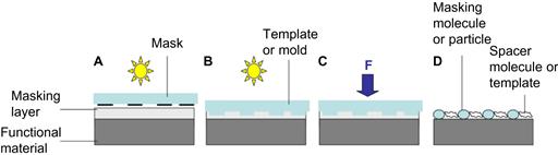
Figure 4.4 Principles of lithographic methods. Lithography utilizes in its strict definition a masking layer. A variety of technologies exist to generate such a masking layer. In most cases the mask or template fabrication process by itself is also a lithographic process using a direct-write method, mostly e-beam lithography. Although stencil masks, e.g., fabricated by techniques such as focused ion-milling are possible, they are not broadly established in manufacturing. The most established technique is (A) photolithography through a so-called chromium mask. Due to the resolution limitations in photolithography, often nanofeatures at the nanometer scale are transferred by nanoimprinting either utilizing a wet process, hardening a polymeric layer through UV exposure (B), or by the application of a (C) thermal process pressing a template into a thermoplastic layer. Alternatively, a masking layer can be generated by (D) self-assembly, where in some of these self-assembly nanolithographic techniques the spacer or template molecule can be omitted. The common aspect of lithographic techniques is here defined as the fact that the pattern generated in the masking layer is subsequently transferred into a functional material.
Reproduced from reference [2] with permission from IOP Publishing.
Within the field of nanotechnology this distinction between lithography and pattern transfer has been weakened in the exploration of novel nanostructuring methods, particularly since techniques such as scanning probe lithography produce a functional nanostructure directly, e.g., by dip-pen lithography. Several outstanding contributions have been made to the field of direct-write scanning probe lithography techniques by the Mirkin Research Group at the Northwestern University Evanston, IL, USA. These researchers utilize multiple cantilevers fabricated by microelectromechanical systems’ technology to increase throughput. One of their specific foci is controlling architectures on the 1–100 nm length scale, demonstrating dip-pen massively parallel pattern transfer in nanomedicine, examples of which are described elsewhere [13–16]. It is, however, too early to categorize any of these lithographic techniques in terms of their importance for the field of miniaturization. According to Figure 4.4 it is much more important to ask the question if a masking or templating layer is needed. The choice of a specific transfer process may deliver certain benefits in respect of the realization of the functional properties of a nanoarray. Of course, this conclusion may be valid for many other designs, too.
4.1.4 Top-Down Nanolithographic Principles
The e-beam direct-write approach offers the highest pattern fidelity (freedom of shape, accuracy, and precision of features and overlay) of all existing top-down nanolithographic methods, but it is mainly used to produce masks and template structures because it is slow. In combination with nanoimprinting, however, it provides a versatile and cost-effective route for the fabrication of many interesting nanodevices. So far, no better technique exists in template manufacture. Although laser interference lithography (LIL) is a much faster and cheaper method for maskless massively parallel patterning, it cannot compete with e-beam lithography in waferscale pattern uniformity and freedom of pattern geometry. These drawbacks of LIL may be due to the lack of suitable large-area mirrors or other suitable interference optics, but 193 nm-deep ultraviolet (DUV) and extreme ultraviolet (EUV) stepper and scanner techniques are emerging lithographic technologies for the semiconductor industry that already offer very high precision and resolution.
Since these technologies are mainly restricted to very high volume production only a brief overview will be given here. Work on these new light sources was initiated by the contributions of Bokor and Oldham [17, 18] amongst others. Maskless techniques, including multiple electron/ion-beam lithography and maskless DUV/EUV interference lithography may at some point overcome the limitation of low throughput in e-beam lithography, at least for specific periodic structures. The selection of a nanolithographic manufacturing technique will always be a compromise between machine cost, speed (wafer throughput) and pattern fidelity (resolution and process stability). In high volume production, where throughput is the major criterion for choosing a specific lithography technique, template replication processes may succeed classical photolithography, but the initial costs making a 1:1 template can be high.
This is similar to the situation in the 1980s, when x-ray lithography (lithography with x-rays as the illumination source) was considered to be the next generation lithography technique for optical lithographic techniques. The definition of an appropriate cost model for nanodevices based on any one of the nanolithographic strategies goes beyond the scope of this overview.
A totally different template-free approach to nanoarray fabrication is also worth mentioning. Materials can be manipulated by low-dose electron beams. If a thin-film polymer is exposed to the transmission electron microscope, the real-time, direct manipulation of the polymer chain aggregate structure becomes possible in two dimensions. The polymer melts, and the chains move by attraction toward preferred electron concentrations within the beam. The principle may be compared to other direct energetic beam-induced surface tension gradients yielding the formation of patterns in material by laser interference metallurgy [19, 20] but the work is, as yet, highly experimental. New machine architectures, novel resists and etch-through processes for lithographic pattern transfer are also being developed, as recently reviewed by Argitis et al. [21]. The Proceedings of SPIE – The International Society for Optical Engineering is an invaluable information resource for details of novel processes, often those which are linked to commercial facilities, e.g., volume 6923 (2008), Advances in Resist Materials and Processing Technology XXV.
4.1.5 Nanolithographic Technologies for the Microelectronics Industry
Deep Ultraviolet (DUV) Lithography
DUV is a key enabling technology which uses 193 nm excimer lasers to produce commercial chips at the 90 nm technology node. Validation of the 193 nm immersion scanner at IMEC’s 300 mm wafer fab facility in Leuven, Belgium, is a clear milestone toward ensuring the availability of a cost-effective technology at 65 nm and may even be extended to the 45 nm node for microelectronics. Many publications have been presented concerning this technological development, of which only a few are cited here [22–26]. The development consists of the definition of a suitable light source, optics and other hardware aspects of such a lithography system, including mask technology, immersion liquid and defect analysis [27].
Extreme Ultraviolet (EUV) Lithography
EUV is considered to be one of the key enabling technologies, much as DUV. The technique is hoped to fill the gap in the semiconductor roadmap towards the 22 nm node for production. A recent trend to overcome the absolute limit of the photolithographic method, is to use the “More than Moore” concept [28–35], hence only a few players are developing EUV as a next generation lithography tool [36–41], including IMEC in Europe and the Lawrence Berkeley National Laboratory in CA, USA. The technique is approaching already the 32-nm node generation of very-large-scale integrated (VLSI) electronics by optical lithography utilizing a 248 nm-laser source, hence EUV is still one of the top candidates for industry to adopt in production. Although investment costs are very high EUV offers very reliable access to high resolution nanostructures, which will clearly be able to satisfy the market needs for high volume nanoelectronic device production for some time to come.
4.1.6 Nanoimprint Technology
Some very good papers have been published concerning the development and application of nanoimprint lithography as a massively parallel pattern transfer technique suitable for industry (principle illustrated in Figure 4.4B and C). Evolved from hot embossing at the microscale, thermoplastic nanoimprint lithography was first developed by Chou’s group [42–44]. Morton et al. have also demonstrated wafer-scale patterning of sub-40 nm diameter and high aspect ratio (> 50 : 1) silicon pillar arrays by nanoimprint and etching [45]. Further developments in this area of research have led to a combination of imprinting and UV exposure, so-called step-and-flash imprinting. This process has been investigated and brought to production standards contributions mainly by Willson (University of Texas, USA) and Resnick (Molecular Imprints, Inc.) who have together published more than 20 papers concerning step-and-flash imprint lithography [46]. Willson’s group continues to develop and optimize materials and processes for this technology [47]. These techniques are at the frontier of nanopatterning and include hybrid techniques such as physical-confined colloidal lithography.
4.1.7 Case Studies: Nanoimprint Applications
Patterned Magnetic Media
Before we start describing the specific nanoimprint processes let us recap some background on patterned magnetic media and the impact of nanoscale in this field of research. Researchers at the Hitachi San Jose Research Center, CA, USA, beautifully presented in Solid State Technology a cover article concerning the patterning of hard disk drives [48]. Given the fact that this vision was presented around two years ago, and the first mention of perpendicular patterned media substrates for data storage was made about 10 years ago, we can conclude that technological development needs transit time (time-to-market) to progress from the research laboratory to industry. The development of robust fabrication technologies is a significant part of this progression [49, 50].
Figure 4.5 illustrates the concept of patterned media (PM), comparing single domain magnetic islands with classical multiple grain media, which suggests a solution to the thermal stability problem by the use of a predefined magnetic dot per bit [51]. Realizing dots at a size of 25 nm diameter and periodicity of 35 nm, within a cost-effective high-volume production process is still a major challenge in nanofabrication. UV-cure nanoimprint lithography is one of the emerging technologies that show the capability to achieve both the high required throughput and resolution for this class of device.
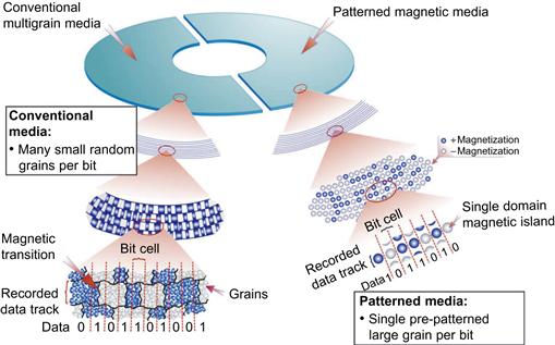
Figure 4.5 Overview of granular versus patterned media (PM) for data storage. Comparing granular media with PM, the novel concept consists of an array of magnetic islands created in the form of a dot. One dot represents a single domain, i.e., spin-direction. One dot is either “written” or “non-written”. In the creation of spatially separated magnetic islands a higher resolution and lower noise level can be achieved than in conventional media.
Reproduced from reference [52] with permission
Moritz et al. have reviewed the use of PM disk fabrication [53]. They demonstrated ultrahigh-density magnetic recording by two ways of patterning: a) direct e-beam lithography and subsequent reactive ion etching, and b) nanoimprinting. The nanoimprint technology delivers polymer arrays with features as small as 30 nm, with a pitch of 60 nm, which are subsequently coated with a Co-Pt multilayer with perpendicular magnetic anisotropy.
Terris and Thomson have reviewed self-assembled PM technology [54], which also requires the development of novel read/write technology. One approach can also be found in MEMS technology based on a cantilever design for atomic force microscopy originally introduced by Rohrer and Binnig [55, 56]. More recent examples of patterned media are given in a review by Terris et al., who also refer to nanoimprinting as one of the emerging possibilities for the cost-effective nanofabrication of PM disks [57], but the authors do not give an opinion as to whether any of these processes will be cost-effective to introduce.
Random Access Memory
A 6 nm half-pitch lines and 0.04 μm2 static random access memory (SRAM) pattern by nanoimprint lithography has been demonstrated by Austin et al. [58]. The authors manufactured a specific high resolution mold by cleavage of a GaAs superlattice grown by molecular beam epitaxy. With these type of patterns they reached the limit of reliable SEM inspection, however, it is suggested that the UV curable nanoimprint process will support line width even smaller than 6 nm.
Surface-Acoustic-Wave Devices
Researchers at the Paul-Drude Institut für Festkörperelektronik, Berlin, Germany, have fabricated surface-acoustic-wave (SAW) transducers operating in the GHz range on LiNbO3 using thermal imprint lithography [59]. The width of the metal lines was 170 nm at a period of 600 nm. Although these SAW devices do not challenge the resolution limit of this technology, which is currently of the order of 10 nm, they are an interesting example of devices having large volume applications in telecommunication.
4.1.8 Emerging Nanolithographic Technologies
Multiple E-Beam/Ion-Beam Lithography
This is a rather different approach to the development of DUV and EUV scanners. It follows the idea of upgrading the wafer throughput of direct e-beam/ion-beam lithography by directing multiple beams in parallel across the wafer area [60–68]. These maskless, massively parallel patterning techniques aim for critical dimensions at the 50 nm line width. Several researchers have demonstrated the potential of such a lithography concept by fabricating multiple-beamlet arrays utilizing MEMS technology. It is not yet possible to assess the position of these emerging technologies on the industrial roadmap.
Templated Nanoarrays
Label-free and high-resolution protein/DNA nanoarrays are an important development within medical diagnostics. Sinensky and Belcher described such an array using Kelvin probe force microscopy as a detection technique [69]. With their method of probing surface-bound target biomolecules, they show that nanoarray diagnostics at 10 nm resolution are potentially possible. Although there is no elaboration of nanolithographic fabrication strategies mentioned in their paper, and their choice of dip-pen nanolithography (DPN) over other nanolithography techniques may be arbitrary, the question of what are the specific requirements for this class of nanoarrays remains. Utilization of one of the following templating techniques is quite interesting and may also be suitable for the fabrication of such nanoarrays.
Reaching the resolution limit of physical templating by top-down lithographic techniques many other substrates including biological are explored. Lee et al., for example, reported the ordering of quantum dots using genetically engineered viruses by fabricating highly ordered composite materials in their publication in Science [70]. In their paper, highly ordered, A7-ZnS, self-supporting viral films are produced. Figure 4.6 gives an overview of the engineering length scales involved in such film. This example demonstrates the extent of the possiblities for self-assembly. A similar process is presented by Huang et al., who demonstrated a programmable assembly of nanoarchitecture, also using genetically engineered viruses [71].
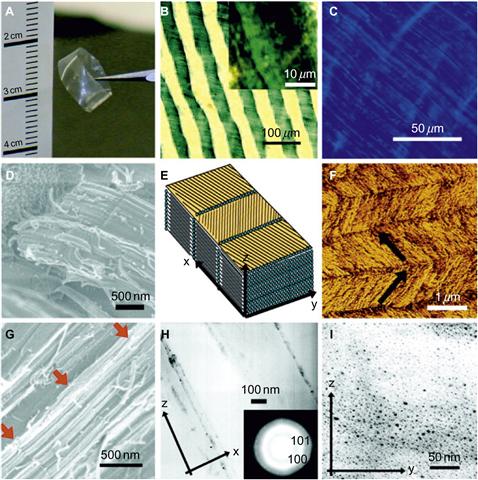
Figure 4.6 Characterization of A7-ZnS film. (A) Photograph of A7-ZnS viral film. (B) POM (20) birefringent dark and bright band patterns (periodic length 72.8 μm) were observed. These band patterns are optically active, and their patterns reverse depending on the angles between polarizer and analyzer. (C) Photoluminescent image, with an excitation wavelength of 350 nm and with filtering below 400 nm, shows 1-μm stripe patterns (50). (D) SEM images of highly packed three-dimensional bulk film structure. (E) Schematic structural diagram of the A7-ZnS composite film. (F) AFM image of the free surface. The phage forms parallel aligned herringbone patterns that have almost right angles between the adjacent director (arrows). (G) SEM image showing the close-packed lamellar structure of phage and nanocrystal layers (diagonal, thick arrows) in the inner areas of the film. (H) Low-resolution TEM image of cross section of A7-ZnS film, with 20 nm × 2 μm ZnS nanocrystal stripe pattern aligned between one phage length in the x–z direction of film; the inset shows an electron diffraction pattern of ZnS wurtzite structure. (I) Low-resolution TEM image of film viewed in the y–z direction, showing ZnS nanocrystals.
Reproduced from reference [70] with permission from the
Alternative templates to phages can be used, such as DNA. In 2006, Feldkamp et al. [193] compiled a review of rational design for DNA nanoarchitectures, in which DNA is used as a building block at the nanometer length scale. This is a technology concept that could offer a large variety of designs for self-assembled supramolecular arrays and other scaffolds, from which it may be possible to form biosynthetic, mechanical and logical nanodevices. To avoid replicating data from this review, we will limit this overview to DNA-based techniques that have been applied to form highly ordered nanoarrays, and have been published over the last few years. For example, Becerril et al. have reported the use of DNA-templates for nickel nanostructures [72]. These nickel nanomaterials may be applied directly as catalytic platforms, or used for the selective binding of protein assemblies. This concept has been demonstrated for the reversible association of a histidine-tagged phosducin-like protein.
Another example of the exploitation of the inherent recognition and self-assembly capabilities of DNA is described by Wang et al. [73]. This group have synthesized and characterized a matrix assembly of single-wall carbon nanotubes (SWNTs), that were functionalized with carboxylic groups and single-stranded DNA (ssDNA) demonstrating negative differential resistance in the biotemplated interfaces of the matrix structure. Combinations of this bio-coordination chemistry will produce a diversity of nanoelectronic effects which have yet to be investigated.
More established fabrication techniques for bio-nanoarrays include the electrochemically controlled assembly of DNA and protein biomolecules onto gold nanoelectrodes, and templating protein assemblies on micro-contact printed surfaces. Huang et al. describe a dynamically configurable biomolecular array, produced by adjusting the electrochemical potential applied at the nanoelectrode allowing for a variety of combinatorial interactions [74]. In other work, Iversen et al. describe a functional nanoarray exploring SNAP-tag proteins affinity bound to patterns of streptavidin modified with BG-biotin that has been stamped onto a surface by micro-contact printing (microCP) [75]. Also electrical-field assisted nanofabrication can be utilized to form multilayered structures composed of biomolecule-derivatized nanoparticles. In the study by Dehlinger et al., a microelectrode-array device facilitates the rapid parallel electrophoretic transport and binding of biotin and streptavidin fluorescent nanoparticles to specific sites on a microarray [76]. Chhabra et al. discuss a spatially addressable multiprotein nanoarray based on aptamer-tagged DNA templated nanoarchi- tectures [77].
Han Yan’s group and their collaborators in the Arizona State University, USA, have published around 50 papers dedicated to DNA-tile-based self-assembly and its application to biosensors. One of these contributions is particularly worth mentioning in the context of nanotechnology, since it describes the phenomenon of multivalency, through which it is possible to assemble multiple molecules while controlling the spacing between them [78]. Another route being explored extensively in self-assembly is the utilization of pore-type structures, of which an overview is given by Hirst et al. [79]. They describe how specific gelator molecules can be assembled for functional nanoscale architectures. Synthetic chemistry that exploits the supramolecular structures that form in molecular gels can be applied as nanostructured scaffold, e.g., for the regrowth of nerve cells, but has also gained interest in nanoelectronics. Use of this type of smart polymeric gel to redefine the limits of biomedical devices has been also described by Chaterji et al., who summarized recent progress in the development and application of polymeric gels based on defining their properties, describing stimuli response and illustrating applications of smartly designed gels to microfluidics [80].
Parallel arrays of geometric nanowells for assembling curtains of DNA with controlled lateral dispersion have been recently described by Visnapuu et al. [81]. In their paper, a process is demonstrated that allows the assembly and visualization of curtains comprising thousands of individual DNA molecules, organized at a diffusion barrier on a lipid bilayer-coated surface. The curtains are made by a combination of geometric barrier pattern with nanofabrication utilizing single-molecule optical microscopy. Unfortunately, the full scale of these fascinating applications of nanoarrays and their fabrication strategies cannot be discussed here. There is, however, much further information available in the literature; for example, Tang et al. describe recognition imaging and highly ordered molecular templating of bacterial S-layer nanoarrays containing affinity tags, and Zhang et al. present the production of nanopatterns by a combination of e-beam lithography and self-assembled monolayers for an antibody nanoarray [82, 83]. In addition, Chen and Li contemplated a record of nanotechnology: moving from microarrays toward nanoarrays [84]. A review of the development of high-throughput methods for functional analysis of diatom genes is given by Montsant et al., and Lynch et al. address functional protein nanoarrays for biomarker profiling [85, 86].
Final mention will be made of the efforts to produce three-dimensional architectures utilizing protein templating. A fairly recent attempt by Allred et al. describes the three-dimensional architecture of inorganic nanoarrays electrodeposited through a surface-layer protein mask [87].
Geometrically constrained inorganic templates as well as biomolecules have been explored for their potential for templating in nanoarrays. For example, nanofabrication of plasmonic structures is reviewed by Henzie et al. who describe the exceptional optical properties present in arrays generated by soft lithography techniques [88]. Hierarchically structured nickel nanoring and hollow sphere arrays were generated by morphology inheritance based on an ordered through-pore template and electrodeposition by Duan et al. [89]. Dipping an alumina template (AAO) into a colloid solution forms a colloidal monolayer with fine structures on the nanoscale. The formation of such morphologies is attributed to preferential growth along the inner wall of the alumina pores. The fine structure of the nanoflakelet originates from a morphology inheritance process of the transitional product Ni(OH)2, which gives the final nanostructured Ni crystals their desirable magnetic properties. These structures may find application in the fields of catalysis, magnetics, optoelectrics, surface-enhanced Raman scattering (SERS), and other new nanodevices.
The self-organized structure of alumina has been utilized for template formation for some time. Her et al. have demonstrated the fabrication of nanostructured titania [90]. Their paper describes the formation of thin film titania by spin-coating in the sol-gel state and subsequent nanoimprinting using an alumina template to yield a dense array of nanopoles. Nanopores in titania were also achieved by utilizing a suitable mold structure. These nanoarrays may also be useful for solar cell, photocatalytic and sensing applications. Kim et al. have demonstrated that fibroblast cells respond to the nanotopology of polymeric surfaces (PMMA) replicated by AAO nanoimprinting [91]. This area of research is potentially of great interest for tissue regeneration of bone. The investigation of osteoblast response to large-area scalable biomaterial nanotopographies has been facilitated by the lithographic techniques discussed here, specifically laser interference lithography as developed at MESA+ [92].
A large number of combinations of materials have been investigated to determine their potential for producing ordered, self-organized nanodot arrays. For example, Meletis and Jiang described the formation of cobalt nanodots in diamond-like carbon thin films that were deposited by magnetron sputtering in a plasma-assisted Ar/CH4 discharge [93]. Cobalt dots of 5 nm diameter, separated by 1–2 nm DLC (diamond like carbon) boundaries and arranged in hexagonal arrays, were produced on silicon substrates. They demonstrate ultrahigh resolution. Such well-ordered magnetic nanodots are promising for the next generation of patterned magnetic media. This class of templated nanoarrays also contains nanoscale structures formed by block copolymer deposition, which generally behaves, in its self-organized ordering, in a similar way to submicron inorganic colloidal self-assembly on surfaces [94, 95].
Colloidal self-assembly has also been used in early applications of massively parallel pattern transfer, known as colloidal, particle, block copolymer or nanosphere lithography, depending on the specific materials being used [96, 97]. However, the self-assembly of a thin film of, for example, a spherical-morphology block copolymer is also mentioned as block copolymer micelle nanolithography, and it can be specifically templated using an array of nanoscale topographical elements that act as surrogates for the minority domains of the block copolymer. This technique has been demonstrated by several authors and is also called guided self-assembly or graphoepitaxy [98–104]. Although it is a nanopatterning technique that is straightforward and fairly simple to use, and has a large variety of design parameters, the difficulty in controlling long-range order and the defects experienced are a major challenge to applying this technique in real-world devices [105]. We also investigated guided self-assembly at the MESA+ Institute for Nanotechnology utilizing block copolymer, nanocrystals and supramolecular systems deposited onto templates fabricated by lithography, such as LIL. This topic will be discussed further, in section 4.1.10.
Confined synthesis is the final class of these novel templated techniques to be mentioned, Fan et al. demonstrated the hierarchical nanofabrication of microporous crystals with ordered mesoporosity, realized through confined growth within a three-dimensionally ordered mesoporous carbon, synthesized by replication of colloidal crystals composed of size-tunable silica beads of about 10–40 nm diameter [106]. Moreover, the authors revealed novel crystal morphologies, consisting of faceted crystal outgrowths from primary crystalline particles, thus providing new insight into constricted crystal growth mechanisms underlying confined synthesis.
4.1.9 Nanolithography in R&D
The formation of patterns by interference lithographic processes (IL) can be carried out with any type of coherent light source. However, IL becomes most interesting if a wavelength is used that reaches pattern periods which are below the resolution limit of an optical photolithographic aligner at λ = 365 nm. This section will describe some of the IL concepts, and presents a case study of this technique, which is often employed in research and development using a deep UV (DUV) laser with a Lloyd’s mirror set-up to produce a cost-effective and stable laser interference lithography (LIL) exposure stage.
DUV Interference Nanolithography
Schattenburg et al. fabricated nanostructures in 1995 by utilizing an Argon-ion laser source at λ = 351.1 nm [107]. The authors suggested interferometric lithography was the tool of choice for patterning large-area, phase-coherent periodic structures with submicron-period gratings and grids, and they postulated many applications, including x-ray and extreme ultraviolet (EUV) transmission gratings, EUV-UV polarizers and filters, field emitter arrays for flat panel displays, as well as in reference grids for e-beam lithography.
An example of using this type of nanolithography of sub-micron sparse hole arrays for field-emission display applications is given by Chen et al. [108]. This paper presents the use of multiple exposure at two different pitches (i.e., angles of incidence), the integration of interferometric and optical lithography by Moiré alignment techniques, and various multi-beam techniques that provide a sparse array and result in a two-dimensional pattern in a single exposure. Later, the same group presents an overview, which considers interferometric lithography to be a nanotechnology enabler in a large variety of applications, but specifically for large-area samples [109]. Several further publications concerning advanced, maskless lithography for the writing of arbitrary non-periodic patterns have been presented by researchers from the Bell Labs (today belonging to Alcatel Lucent, USA) [110–112], and another, more recent example of using interference in combination with catalytic etching is given by Choi et al. [113].
EUV Interference Nanolithography
Solak discussed how this technique produces periodic nano-structures with resolution below 20 nm [114]. Earlier work by Choksi et al. introduced the concept of maskless extreme ultraviolet lithography [115], and Olav Solgaard and co-workers at Stanford University, USA, continued these developments, publishing work on analytical models for several micromirror array configurations and later on spatial light modulators for maskless lithography [116, 117]. More recent progress in extreme ultraviolet interferometric and holographic lithography is published in several contributions by Cerrina’s group at the University of Wisconsin-Madison, USA [118–120].
Atom Lithography
Laser focusing of chromium atoms for nanostructure fabrication was first decribed by McClelland et al. [121]. This work was followed up by a publication on a fast, deterministic source of single chromium atoms [122]. So far, this topic is progressing very slowly in the scientific community, with just one additional publication concerning the principle of Stern–Gerlach interferometry [123].
4.1.10 LIL Development at MESA+ NanoLab NL
A Lloyd’s mirror laser set-up utilizing a cost-effective 266 nm DUV laser has proved to be a simple and useful tool for the fabrication of nanoarrays which have structural resolution down to the sub-500 nm regime. Combinations of reactive ion etching can be explored using the LIL resist as an etch mask. LIL was previously demonstrated by researchers at the MESA+ for the generation of sieves, photonic crystal structures and patterned magnetic media (PM) [124–128]. Figure 4.7 shows the concept for LIL exposure, and an example of a resulting patterned media in the inset.
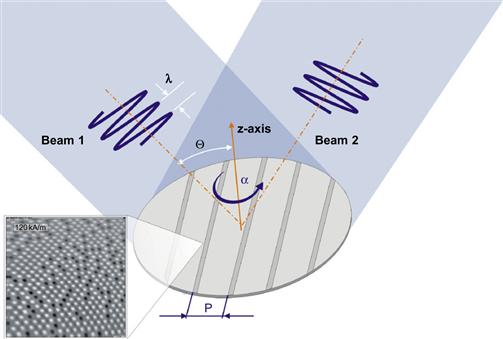
Figure 4.7 Artist impression of laser interference lithography for the fabrication of PM. The pattern period (P) is defined by the wavelength (λ) and the angle of incidence (Θ) while the possibility to rotate the substrate allows two-dimensional arrays such as dots, hexagones, and Moiré-type patterns through a multi-exposure at different substrate rotations (α). LIL has been applied to fabricate the magnetic structure shown here in the inset, which is described in detail by Murillo et al. [127].
Reproduced from reference [2] with permission from IOP Publishing.
The NanoLab NL cleanroom facility at University of Twente’s MESA+ Institute for Nanotechnology, Enschede, The Netherlands, has installed an optical table that is appropriate for conducting laser interference lithography with the ability to change the experimental conditions for a variety of different projects. Based on earlier research by Cheng et al., who investigated LIL templates for the fabrication of nanostructures with long-range order using block copolymer lithography, for example, the MESA+ set-up has also been applied for such hybrid lithographic techniques [129]. Dziomkina et al. have investigated the patterning of surfaces where LIL assists the symmetry control of polymer colloidal monolayers and crystals formed by electrophoretic deposition [130]. Similar processes utilizing LIL were also demonstrated by other groups, e.g., Kim et al. [131].
The MESA+ LIL system was used for preliminary templating experiments in the layer-by-layer deposition of supramolecular assemblies. However, LIL has now been replaced by nanoimprint lithography (NIL) techniques based on e-beam lithographically produced masters for research into this hybrid approach [132]. Figure 4.8 shows the set-up as used at NanoLab NL. The optical set-up allows full scale 4-in. wafer handling.
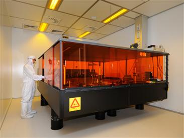
Figure 4.8 NanoLab NL cleanroom facility at MESA+ Institute for Nanotechnology. Full scale 4-in. wafer handling at the LIL set-up.
Image courtesy: H.A.G.M. van Wolferen, University of Twente, 2011.
A variety of current investigations of nanostructure applications continue to rely on LIL as a nanolithographic tool at MESA+, as is mentioned in the following section.
Multi-exposures and Novel Resist Systems for 266 nm LIL
This section presents some additional results that have been achieved in the nanofabrication of large-area nanostructured surfaces, and explores the capabilities of specific resists and multi-exposure approaches. Both method and materials are briefly summarized here.
Method/Materials
The generation of one-dimensional (gratings), two-dimensional (arrays of dots) and mesoscale quasi-regular discontinuous nanoarrays by LIL exposure into a resist can be described briefly as follows. A standard (100) p-type, polished prime silicon wafer is used as the substrate. LIL is operated at 266 nm, utilizing the aforementioned continuous-wave laser source as an exposure tool. This lithographic process line, consisting spin coating, soft-bake, LIL exposure, post-exposure-bake and wet development, is described in detail earlier [133]. Three types of resist were employed to evaluate their performance in the LIL set-up. The first, a standard i-line photolithographic resist system OiR 907-13 (from Fujifilm, formerly called Olin) was diluted to a suitable concentration to be spin-coated and produce a film thickness below 200 nm. The use of diluted Olin for 266 nm-LIL has also been described by Murillo et al. [127]. Although the resist is not very stable after dilution, we applied this resist system for multi-exposure experiments, producing a mesoscale quasi-regular nanoarray (for an overview of nanoarray definitions see Figure 4.2 and Figure 4.3).
The second set of conditions for producing nanogratings by a single exposure used a positive chemical amplified resist, PEK500 (Sumitomo Chemical). This was set up for a systematic evaluation of scaling line width, pattern period (pitch) and pattern depth (aspect ratio) during pattern transfer by RIE. A full record of this fabrication technology exploring positive chemical-amplified resist (p-CAR) has been given previously [133]. Finally, a third type of resist, the negative acting MA-N2403 (Microresist) demonstrated the potential for using high-contrast resists during LIL multi-exposures to generate integrated micro-nanoarrays.
Results
Multiple exposure experiments at two different angles of incidence (14° and 15.4°) and repetition of these exposures after a substrate rotation of 90° were carried out to achieve a latent nanopattern grey-scale image in the OiR photoresist, here acting as a low-contrast resist at λ = 266 nm to generate Moiré-type features. Subsequently, the resist was developed in a single step in an immersion bath for 1 min using standard OPD4262 positive resist developer. Figure 4.9 shows how these structures evolved from interference between the multiple set of exposures.
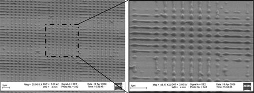
Figure 4.9 Four multiple exposures resulting in a spatially defined pattern of micrometer and nanometer sized elements within a quasi-regular array, previously also defined as a discontiuous nanoarray. The mesoscale pattern can be uniformly fabricated across an area of approximately 2 × 2 cm2.
Image courtesy: M. Smithers, University of Twente, 2006.
Figure 4.10 demonstrates the potential of p-CAR pattern transfer by parallel plate reactive ion for etching a dot pattern into a layer of silicon nitride, aiming at a pattern period (pitch) of 38 nm, which refers to an angle of incidence of 20.48λ in the two orthogonal exposures. The dots can be subsequently coated with magnetic, conducting material. Previously, these nanoarrays were fabricated using an orthogonal exposure in OiR resist. Subsequently, the samples were used in a method for field-emission distance control by le Febre et al. [128]. Applying the improved LIL process utilizing p-CAR resist, as shown here, will further support well-controlled sample preparation for PM recording experiments.
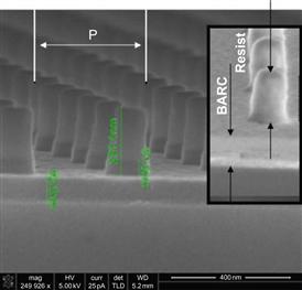
Figure 4.10 Dot array on silicon nitride. Orthogonal exposure into resist on bottom antireflection coating (BARC) transfer layer at 20.48° angle of incidence resulting in a periodic pattern in the resist with a pitch (P) of 380 nm (inset shows an example of the resist prior to the pattern transfer etch). The scanning electron micrography (SEM) shows a cross-sectional view of the silicon substrate at nearly 90° of the SEM holder producing a full-height view on the dots etched partly into the silicon nitride. The resist/BARC mask has not yet been removed.
Image courtesy: J.G.M. Sanderink, University of Twente, 2007.
Figure 4.11 shows the nanograting pattern fidelity of the line width/space ratio at five different points across the diameter of a 4-in. silicon wafer, as measured by scanning electron microscopy. This result demonstrates the difficulty of controlling the uniformity of such continuous nanoarrays over a large manufacturing area. This aspect remains a challenge for the exposure tool designer in selecting suitable optics.
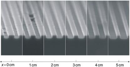
Figure 4.11 Single exposure at 40.6λ angle of incidence [134]. The scanning electron micrographs are taken on the middle line of the wafer to demonstrate the pattern distortion due to optical aberrations. However, the usable area of high uniformity still stretches across a few cm2 during the full 4-in. wafer scale exposure process. Areas of high pattern fidelity vary with the angle of incidence applied and the total mirror surface area being exposed uniformly by the source.
Image courtesy: M. Domanski, University of Twente, 2008. Reproduced from reference [2] with permission from IOP Publishing.
When replacing the low-contrast OiR resist with a high-contrast negative resist, e.g., the MA-N2403 (Microresist) used here, a highly-defined integrated micro-nanoarray pattern results from the same type of multi-exposure carried out in the previous experiment (Figure 4.9). A micro-nanoarray produced by using the negative resist is presented in Figure 4.12.
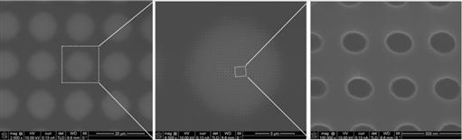
Figure 4.12 Nanohole-microarray formed by high-contrast negative resist LIL-multi-exposure producing nanoholes at 20° angle of incidence. Details of this processing conditions are disclosed.
Image courtesy: H.A.G.M. van Wolferen, University of Twente, 2009.
4.1.11 Case Study: Laser Interference Lithography Nanoarrays for Cell Biology
Specific experiments have been designed to study the interaction of biological material (tissue, blood, proteins) with nanostructured surfaces. First, systematically scaled, large-area nanogratings were fabricated by solvent cast replication from the large-area (2 × 2 cm2) master, by the LIL process and subsequent silicon etching. Secondly, these nanostructured surfaces were investigated for their cell response. The fabrication details are communicated elsewhere [92, 135], as are the full details of the biological experiment [92, 136]. Here, we only wish to stress the multitude of processing possibilities of LIL nanolithography.
Several studies have demonstrated that biological processes can be activated when a surface has a specific nanotopography [137, 138]. Kim et al., for example, cultured fibroblasts on PMMA surfaces that were nanostructured using AAO as a template for nanoimprinting [91]. Recent work by van Delft et al. showed that e-beam lithography can be applied to manufacture a template containing nanopatterned fields of 500 × 500 μm2 that were reproduced in polystyrene and subsequently tested for their cell response [139]. The lines and spaces of the nanopattern within each field had various pitches, but always at a line width-to-space ratio of 1:1. Original work relates back to micropatterned surfaces for cell alignment in cell culture [140].
Lamers et al. systematically investigated the size and geometrical dependence of the biological response in cell culture experiments in the context of tooth implants. LIL is used in this context for its capability for large-area nanoarray formation, and also its potential to be used for simple and cheap maskless exposure onto non-flat surfaces.
Large-area LIL nanoarrays with a diversity of line width, pattern period and depth have been evaluated for their fibroblast, osteoblast and microphage response [92]. Initial results concerning the fabrication process for artificial nanotopography in medical grade titanium utilizing LIL has been presented by Domanski et al. [141]. Large-area patterning supported by the LIL technique is of particular importance in gaining statistically relevant results from the cell culture proliferation experiments. Substrates produced by e-beam lithography are often too small in surface area, only allowing a few cells to attach to one specific pattern.
4.1.12 Concluding Remarks on Emerging Nanolithography
In lithographic processes the control of the transfer of a layout first into a masking layer (resist) and then to a functional material allows the creation of devices with an enormous variety of capabilities. Of course, electronics remains at the frontier of lithographic techniques, reaching the scale of a few nanometers. Other disciplines are catching up quickly and even bring their own lithographic techniques.
A broad choice of techniques exists, of which only a few will be selected to lead market innovation in electronics. EUV is probably the preferred technique. In research investigating nanoscale behaviour in specific (e.g., PMs for magnetic data storage) and niche manufacturing (e.g., optical devices), templated techniques are gaining in significance. Nanoimprint lithography is gradually replacing mainstream UV-photolithography. When it comes to nanoarrays, interference lithography has become a valuable addition to the range of techniques.
The ability of chemical and biological substrates to coordinate ordering at the molecular scale is also about to reach the level of control required in industry. However, this is not yet on the wafer scale which we are used to in commercial applications. In respect to further deepening our understanding of controlling device functions at nanoscale dimensions, research in the field of nanolithography will remain extremely diverse and may be mainly guided by which techniques are to hand as opposed to a choice by design. It is, therefore, of particular importance to develop new cost-to-lithographic performance models, which give the designer of novel devices some insight into this diversity. Yet the choice between a well-established but limited process line, e.g., as is found in microelectronics complementary metal-oxide semiconductors (CMOS), or a novel lithography that capitalizes on the advantage of delivering very unique devices’ properties is not an easy one. The multitude of parameters involved in establishing a production line makes such choice difficult.
The next direct-write techniques, e.g., using focused ion beams, are being developed. Their extension to an out-of-plane dimension may be either supported by stacking (assembly), multilayer processing, folding, or three-dimensional lithographic techniques such as two-photon lithography [142]. However, so far only a few technologies have shown true potential for creating three-dimensional crystal lattices across the different length scales from the nanometer to the centimeter, one of which is holographic lithography [143]. Whether these processes will find real application beyond photonic crystals is not yet known. The patterning of nanoarrays, e.g., for multilayers which are useful to perpendicular magnetic recording, x-ray diffraction, EUV diffusers and SAW devices, as well as surface modification by nanostructuring of implant materials, is, however, being actively investigated in our laboratory at the MESA+.
4.2 Nanomaterials
The integration of structural elements using lithographic patterning techniques aims for a more complex apparatus, which can be at various length scales, for example hand-held equipment. However, as mentioned above, pillars, holes or wires that are fabricated at the nanoscale have already shown unique properties, and ordering these in specific arrangements results in novel phenomena. Such materials are called metamaterials, an example of which is a material with a negative refractive index, creating an artificial structure. These exciting material properties bring about new opportunities for applications.
A functional device or system which demands some level of ordering in its materials also requires a carefully designed manufacturing process. Here, we will present an overview of nanolithographic techniques for oxides. Nanoscale designed oxides show great promise for energy storage and energy converting systems, and are thus a very important class of novel materials. Bio-inspired, templated oxides will be described in relation to other nanolithographic techniques, as will the way in which (nano)structured materials can deliver specific functionality at the interface with biological materials. We can look for new applications for these materials including within medicine, where the properties of oxide nanostructures as a biocompatible material are explored. Photonic crystals, for example, can be applied in medical diagnostic devices which are used in direct contact with complex biological samples, e.g., blood. In this section, oxide metamaterials are introduced and the emerging technologies which are employed for their fabrication, together with the medical devices that utilize oxide nanoarrays, will be discussed.
4.2.1 Ordered Oxides
It is the objective of this section to review nanolithographic techniques for producing oxide nanoarrays, specifically inorganic oxides. Although many interesting (polymeric) organic oxide arrays exist and are being investigated for medical applications, for example, thiolated polyethylene oxide as a non-fouling element for nano-patterned biodevices, we will not be able to discuss these here [144]. Some examples have already been given, such as nanostructuring of a polymer that is used as a colloidal masking layer (nanosphere lithography, see Figure 4.4D), where polystyrene beads protect the polymer film in a subsequently applied O2 plasma etch process. Initially these polymerical films may be deposited by plasma enhanced chemical vapor deposition (PECVD) [145]. Another example is a highly experimental technique that utilizes nanobubbles as templates for the fabrication of nanoporous films of polypyrrole (PPy) on highly ordered pyrolytic graphite (HOPG) [146]. PPy is widely used as a conductive polymer in medicine, e.g., PPy-implants are suitable for neural prosthetics [147]. This text will not discuss oxide nanoarrays from a materials engineering point of view, although this has an extensive history of making textured materials through chemical synthesis. This book will, however, reflect on these systems from the viewpoint of a device designer who is screening the emerging nanotechnologies for nanostructured oxide devices. Therefore, we will first introduce the terminology as used in this context and then present some background on naturally occurring oxides. Our discussion will consider how metamaterials complement and enhance device functionality, making particular reference to the impact of nanoscale-provoked functionality in innovative devices in nanomedical applications.
4.2.2 Oxide Nanoarrays: Definitions and Background
Natural versus Artificial Oxide Nanoarrays
Before discussing the various oxide materials that form nanoarrays, we must first define what is meant by the term “oxide” in this context. Turning to inorganic chemistry, an oxide is a chemical compound formed from an element and at least one oxygen atom. Materials can also be classified by their oxidation state (the number of valence electrons in the chemical compound). Nearly all elements can form oxides when they are exposed to oxygen. Noble metals such as gold or platinum form oxides with greater difficulty, but these do exist. Oxides can be also gaseous, but we will only consider solid oxides.
Oxides can be amorphous (for example window glass) or crystalline (quartz, sapphire). Natural silicon oxide formed on a silicon surface is also amorphous, and is normally removed from wafers prior to processing. In this context, there is no need to explain the dielectric properties of silica and its benefits or disadvantages in electronic applications. In other applications, amorphous oxides have been used as a platform for releasing molecules or electrons from its matrix. For example, in drug delivery, highly defined oxides have replaced the polymeric coatings which were previously used. Such a polymer-free platform is used for drug loading in cardiovascular stents [148]. Additionally, biomedical devices for neural stimulation have been based on oxide thin-film technology. In this application, a Teflon-type substrate is covered with a gold/iridium oxide film. The gold layer acts as current collector, and the iridium oxide as an electrochemical actuator. The intrinsic material microstructure plays an important role in enabling a low-resistance interface [149]. Another more recent example for an application of iridium oxides (IrOx) is given by Huang et al., who developed an IrOx micro pH sensor array [150].
Such miniaturized sensors could be used in chemical, food and bio-material devices. The authors present the design and fabrication process of an amorphous, IrOx, thin film, pH sensor array on flexible polymer substrates in their paper, so the utilization of amorphous oxides as micro- and mesoporous materials have therefore already found their way into applications. Most likely these materials will not be called nanoarrays, although their intrinsic microstructure means that they could be considered as such (e.g., see Figure 3.7, Chapter 3, Section 3.3.6), as could natural crystalline oxides. The properties and classifications of oxides is too broad a field to be discussed here, so this section will be restricted to some oxides that have been described in the literature as an artificially manufactured material. Examples are selected on the basis of their specific optical properties and the application of such oxide nanoarrays in the medical field. Figure 4.13 depicts the four different material types that can also be manipulated into nanoarrays: (A) crystalline, (B) polycrystalline, (C) amorphous and (D) layered composites.
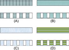
Figure 4.13 Definition of nanoarrays: (A) crystalline, (B) polycrystalline or interdispersed composite, (C) amorphous, and (D) layered composite materials and their according nanoarray by lithographic patterning.
Reproduced from reference [3].
Oxide Metamaterials: How Do They Differ from Nanoarrays?
One could argue whether the term nanoarray is really required. Both artificially formed and natural materials show ordering. At the nanoscale, many materials show a certain level of order and with respect to engineering, one likes to give the new field of research that investigates these phenomena a new name: nanotechnology. Hence the arrays being investigated at this scale are called nanoarrays. Most are formed by engineered processes and therefore these materials may exhibit some property that differs from naturally occurring structures, e.g., structures with a negative refractive index. However, since these artificial materials are generally known as called metamaterials, their properties may not always be derived from the nanoscale. The term nanoarray is most often used for nanoscale engineered metamaterials which contain a high ordering of a nanoscale object, such as a pillar or a hole. This is a very exciting class of materials. There is also a wide variety of such materials that are grown epitaxially (gaining their order from the underlying crystalline substrate). After a short general overview given in the next two subsections, the core of this section discusses nanoarrays from oxides that are formed by manipulation of material by a lithographic-type process, and have subsequently demonstrated exceptional material properties.
Curiosity-Driven Research on Nanoscale Metamaterials
A general theory of electromagnetic propagation in periodically stratified media has been proposed by Yeh et al. [151]. It was found that point and line defects could be introduced into the structure to localize and direct optical waves. Another article describing the optical properties of nanostructured optical materials was published by Gehr and Boyd [152]. These are just two publications of the many which discuss these phenomena. When going deeper into this topic one should realize that all applications start here. Industry will probably not invest directly in research into the fundamental behavior of matter at an energy boundary encompassed by the material’s properties. Fortunately, questions concerning these underlying working principles and rules of nature can be investigated by independent and curiosity-driven scientists, due to public funding, if this continues.
Application-Driven Research on Nanoscale Oxide Metamaterials
Enhancing the optical properties of integrated sensing devices is an interesting research topic. Rhenium oxide films have been characterized by Cazzanelli et al. [153], and the fabrication and characterization of cerium oxide (CeO2) thin films for ultraviolet sensing applications was recently presented by Wang et al. [154]. The latter use oxide deposition by reactive oxygen ion-beam assisted e-beam evaporation to produce cerium oxides with refractive index enhanced from ca. 1.8 to 2.2. This ion-assisted deposition method also increases electrical resistivity by a factor of ten. This was a new concept for photodiode devices. A gain in photocurrent of 100 times and a fast photoresponse under a 405 nm UV exposure had been discovered. These parameters, probably both linked to the material’s specific stoichiometry and crystal structure, are measurable by x-ray photoelectron spectroscopy and x-ray diffraction.
Pulsed laser deposition (PLD) is an emerging material deposition method. Nanoporous cerium oxide thin films were desposited by PLD and used for glucose biosensors. The sensors containing such films showed enhanced enzyme affinity for converting immobilized glucose oxidase (GOx) to glucose, as reported by Saha et al. [155]. They studied the surface morphology of these PLD CeO2 films by atomic force microscopy. Their results show that CeO2 nanoporous films can be utilized in glucose sensing applications without the need for additional surface functionalization. Another example of this type of sensor was presented by Ansari et al. [156], in a feasibility study of glucose oxidase (GOx) immobilized tin oxide thin films, consisting of nano-baskets, for glucose sensing. Their approach used anodized alumina pores of 80 nm diameter as a template for the plasma enhanced chemical vapor deposition (PECVD) of tin oxide (SnO2). This process formed nano-baskets. The GOx was immobilized by physical adsorption from solution, and elemental analysis of the films revealed the GOx was covalently attached to the tin oxide. This sensor design, based on a crystalline film with basket-like (nano-sized) structures, demonstrated higher sensitivity in comparison to other structures.
Investigating conducting metal oxides, Rhodes et al. reported initial observations of surface plasmon resonance (SPR) [157]. They claimed that the systematic variability of many conducting metal oxide composites suggests significantly advanced film properties and innovative possibilities for versatile and sensitive chemical sensing applications. The properties of nanoscale oxide metamaterials and their fabrication processes could potentially be utilized in devices other than sensors. In 2004, Vayssieres described a novel growth concept, and a low-temperature aqueous chemical growth thin-film processing technique that may lead to a new generation of smart and functional metal oxide particulate thin films and coatings, called purpose-built materials [158].
4.2.3 Principles of Oxide Nanoarray Fabrication
In Chapter 3 we referred to the patterning of oxides such as ceramics, zirconia or alumina, as well as more complex oxide composites that are partly or fully crystalline. These materials are difficult to pattern by etching techniques. Normally, ceramics are put into their desired shapes prior to sintering by ceramic-forming techniques such as slip-casting. In the top-down approach, thin-film oxides were nearly always patterned by physical ion bombardment, i.e., ion milling techniques, to create an artificial structure. This method is very inefficient, and more recently chemically-assisted reactive ion etching through appropriate masks, together with novel templating techniques, including lithographically assisted templating, have been under development (e.g., MIMIC, see Chapter 3, Section 3.3.3). Because ceramics are difficult to manufacture from the top-down, most research attention has been given to the design of morphology through a materials engineering approach, which aims to control the intrinsic microstructure from the bottom up. Some examples of nanoporous sensor designs have been given already. Pre-1995, the bottom-up approach in this field would have been treated as coordination chemistry, and would probably have used metal-ion coordination either by a wet-chemical technique or from a gaseous precursor [159]. However, to generate metamaterials with more engineering versatility, recent advances in deposition techniques such as pulsed laser deposition (PLD) present the possibility of stoichiometrically defined materials from ceramic targets. These targets are often prepared from pressed powders or by ceramic slip casting. PLD allows the deposition of highly innovative multilayer materials. Ravichandran et al., for example, contributed to the understanding of the nature of electronic effective mass in double-doped SrTiO3 by this technique [160].
Sol-gel, and electrochemical processes (such as the anodic oxidation of aluminum) can also be used to form highly ordered oxide films with specific morphology. Much research is currently being devoted to investigating techniques for patterning oxide films at the nanoscale. Some studies discuss the intrinsic modification of crystal structure through laser radiation. Beke et al., for example, investigated laser treated vanadium oxide sols [161, 162]. Their x-ray photoelectron spectroscopy and x-ray diffraction studies reveal how the original xerogel particle structure changes into irregularly shaped, layer-structured V2O5. Depending on the laser power used, different material structure was created. Some specific examples of non-lithographic templating have already been mentioned in section 4.1.8. The following sub-sections will focus on top-down lithographically-assisted, collodial, bio-inspired and biotemplated techniques for oxide nanoarrays.
Lithographic-Assisted Oxide Nanoarrays
In this class of patterning techniques two controversial approaches have been discussed for many years. These are the direct-write lithography approach, which is normally used in industry for the primary patterning of a mask, and lithography incorporating the pattern transfer through a mask. There is a wide range of available methods, and the question is which of them could be applied to creating oxide nanoarrays. So-called electro-pen and dip-pen nanolithographic techniques, for example, are likely candidates [163, 164]. These nanochemistry and scanning probe lithographies were reviewed by Garcia et al. [165] among others.
I will restrict this discussion to two examples of very controversial concepts: oxide nanoarrays etched through a large-area mask, and focused ion beam (FIB) milling for prototyping integrated optical devices from novel materials.
An example of the first concept is the fabrication of nanoporous silica films by utilizing a chromium pattern transfer etch mask formed by particle lithography [166]. FIB, the second concept, has been applied by Lin et al. to experimentally confirm their simulations for two-dimensional nonlinear photonic crystals using barium titanate thin films [167]. Lee et al. have also used this technique to measure the Brillouin gain-coefficient for a bismuth-oxide-based photonic crystal fiber under significant beam reflection at splicing points [168]. Unfortunately, there are no specific industrial applications to date of these lithographic-assisted oxide nanoarray systems on the market.
Bio-inspired and Biotemplated Oxide Nanoarrays
Even further from industrial applications are the biomimetic approaches to material synthesis, as for example, reported by de Guire et al. [169]. Oxide thin films are deposited on organic self-assembled monolayers (SAM) from solutions at temperatures below 100°C. Dense thin films of ZnO were achieved under basic conditions. TiO2, ZrO2 and Y2O3, which were formed from acidic solutions, produced better films. Taking the technique a step further, this SAM layer can be pre-patterend by lithographic techniques such as nanoimprinting. However, direct write approaches and laser interferences may also be used in combinations with SAMs; for example, see Yasseri et al. or Friebel et al. [170, 171]. Alternatively, dip-pen lithography may be used to deposite SAMs or sol-gels locally onto a surface in a similar way to that described for matrix-assisted dip-pen nanolithography and polymer-pen lithography by Huang et al. [150]. A combination of the two processes (biotemplating and lithography) may present us with a design route for an even higher hierachical level of structural components than currently exists in microelectronics. Another approach to templating is the use of biological material such as aminoacids, peptides, DNA, microtubules, silk, etc. Viruses or bacteria have also been exploited as non-planar templates, e.g., for the formation of advanced, virus-free nanoparticles demonstrating virus-templated silica nanoparticles through mineralizaton of a cage-like viral bionanoparticle, such as the cowpea mosaic virus [172].
These systems have a natural tendency to form highly ordered features that can be utilized for the articifical patterning of engineered materials. Han et al., for example, utilized natural templates such as peacock feathers for novel photonic crystals that incorporate Nano-CdS, thus producing novel hybrid photonic crystal materials [173]. Affiliated with this research group, Su et al. presented the biogenic synthesis of highly ordered oxides achieved by stepwise bioredox/artificial oxygenation using egg-shell membranes (ESM) as a template [174]. Another recent example is the work of Zhang et al., who presented a novel photoanode structure templated from butterfly wing scales to embed zinc oxide (ZnO) nanoparticles, replicating the naturally occurring nanostructure in these systems by in-situ ZnO nucleation at suitable binding sides on the template [175].
Although access to state-of-the-art analytical equipment, such as high resolution scanning electron microscopy, is necessary in this field of research, these contributions clearly demonstrate that innovation through nanotechnology research does not always need large capital resources. Any of these template techniques have the goal of producing functional hybrid nanocomposites with hierarchical micro-nanostructure. Biomimetics of photonic nanostructures were introduced as an engineering approach by the Parker and Townley methodology [176]. See also the review “Natural photonics for industrial inspiration” [177]. A study of biomimetic interfaces with high-performance optics in the deep-UV light range has been performed Lohmüller et al. [178], and Balci et al. demonstrated the catalytic coating of virus particles with zinc oxide utilizing a rod-shaped tobacco mosaic virus. These electrodeless deposited materials show cathodoluminescence [179]. The generation of oxide nanopatterns by combining the self-assembly of S-layer proteins and the area-selective atomic layer deposition of metal-oxide-based high-k materials was demonstrated by Liu et al. [180]. They investigated the deposition of hafnium oxide in the pores of the octadecyltrichlorosilane (ODTS)-modified S-layer proteins on silicon. These materials will facilitate further miniaturization of logic and memory nanoelectronic devices.
Many groups are currently exploring biology and biomolecular engineering for potential technical benefits to nanofabrication. A variety of these biomolecular assembly strategies have demonstrated groundbreaking results [181]. The developments of these novel bio-hybrid concepts also indicate the possibility of a new era of highly sensitive, low-cost diagnostic devices and efficient novel medical therapies.
4.2.4 Ordered Oxides in Medical Applications
Actually, nanofeatures in metal exhibiting exceptional optical behavior are already much more common than nanostructures in oxides. Experimental and simulated near-field images of a nanohole array in gold films has been reported by Gao et al. [182], who give “Direct evidence for surface plasmon-mediated enhanced light transmission though metallic nanohole arrays”. One would like to argue that it is the actual hole structure which causes the enhanced light transmission, and not the metal. This hypothesis has been tested experimentally by creating the same structural features in silicon, which did not exhibit the same effect. Therefore, the combination of the material and the nanostructuring led to the desired effect. Such type of designs were also characterized by a prominent diffusion phenomenon in the near ultraviolet region [183]. Many oxides demonstrate exceptional optical behavior, such as the anomalous enhancement of Raman scattering that was detected for tungsten oxide thin films deposited on indium tin oxide (ITO) coated glasses during special annealing treatment [184].
Novel Nanoarrays in Diagnostics
The fabrication of inexpensive but highly accurate and sensitive diagnostic devices is dependent on the development of novel fabrication technology. Nanotechnology moves diagnostics from microarrays towards nanoarrays for high-throughput analysis. Further downscaling would be advantageous for point-of-care application and field applications [185].
By indirectly exploiting intrinsically confined oxide nanoarrays, scientists at the University of Illinois, USA, have developed a disposable, microplate-based optical biosensor that is capable of detecting protein-DNA interactions. The photonic crystals biosensor consists a hybrid material. First a low-refractive-index polymer grating is manufactured and coated with high-refractive-index titanium oxide. The grating structure is positioned on the bottom of a standard 384-well microplate, in which each well functions as a miniaturized test tube [186]. In the light of this paper, protein nanopatterns have been utilized to improve immunodetection sensitivity. The sensor surface is prepared with bioadhesive domains of nanometric dimensions in a nonadhesive matrix which is formed by means of colloidal lithography [187].
Perspectives on Nanoarray in Therapy
Engineered nanomaterials for biophotonic applications to improve sensing, imaging and therapeutics are clearly feasible [188], but there seems to be no specific examples of the use of oxide nanoarrays in this regard in the literature. When referring to the use of organized systems there may be room for improvement in photodynamic therapies. Furthermore, we could modulate the release rate of a therapeutic agent from a membrane (or a vesicle) by tuning its pore size, e.g., by modulation of these properties by means of optoacoustic or optoelectronic phenomena. By using such smart biomaterials, for example as skin-scaffolds, photo-stimulation may support the wound-healing process. More realistic at this stage are optical means of material functionalization prior to contact with biological material. Future applications may include opportunities in scaffolds for cell-growth, substrates for cell culture, experiments in biomedical-related diffractive optics and optical interfaces, and substrates for tensegrity studies. Perry et al. gives an example for nano- and micropatterning of optically transparent, mechanically robust, biocompatible silk fibroin films [189].
4.3 Where Are We?
Trillions of nanosystems are packaged with ease in our body. Nature has mastered the assembly of nanosystems into workable machines through evolution. In the engineering sciences we can learn from nature, and use our findings as a source of inspiration for packaging artificial, higher assembled architecture devices. Of course, there is no competition between nature and engineering – it is synergy. Sometimes applying the concepts of nature and building from the bottom up would simply take too much time and the top-down approach works better. In the next decade it is important that the engineering sciences deliver appropriate design rules for industry to justify investments in nanotechnology. This survey of design rules for nanoengineering must, and will be, clearly supported by governmental incentives for creative research and development in this field. Based on such research incentives the investment risk for industries can be further lowered, specifically in areas which have long development cycles, such as medicine and high-tech applications. Currently there are no clear solutions for novel products that require first appropriate packaging of nanodevices as such that they can interact within real world devices.
4.4 Where to Go from Here?
In the past decade more and more developments have gone nano, and research on this topic has clearly intensified in many working fields. Nano has made a profound impact on medicine and health care industries, such as biomedical diagnostics. Investments in nano already presents us with novel opportunities in these branches of science, although products have not yet emerged on the market. It has been the objective of this chapter to reflect and highlight current trends of nanofabrication, and identify key issues and challenges for making nanomaterials with a high structural order – the so-called nanoarrays. We have covered several aspects of the fabrication of such metamaterials.
The implementation of novel nanofabrication strategies in medicine will, however, strongly depend on appropriate medical technology assessment protocols which incorporate materials screening through a multidisciplinary approach. New materials discovered in the Natural and Engineering sciences often take more than 10 years to appear in Life Sciences applications. Materials in contact with the human body are currently benefitting the most from these innovative nanosolutions. However, at least three aspects of such new developments in medicine must be investigated, besides their direct functional purpose. They are:
1. long-term safety in production and use of the nanomaterials,
2. match with a patient’s personal profile, and
3. functionality throughout a timescale that meets the patient’s needs in a sustained and reliable manner.
Healthcare professionals will only implement a new material in medical practice if these criteria are fulfilled. It is therefore an engineer’s responsibility to create boundary conditions that will allow the assessment of a material’s usefulness for this application as early as possible. Multiscale physics, exploiting a wide variety of advanced computational and experimental tools, is one approach to faster materials implementation and aims at a better understanding, a better description and – in medicine – a better control of the properties of these materials in biological processes. It allows the prediction of material properties or system behavior based on a knowledge of the atomic structure and properties of elementary processes. Photocatalytic activity of titania nanohole arrays has been demonstrated, for example, by Hamaguchi et al. [190], and PLD on colloidal templates has been evaluated for its ability to produce photocatalytic active amorphous TiO2 nanocolumn arrays [191]. These titanium nanoarrays can be deposited on nearly any substrate and although they have only so far been discussed for possible use as a self-cleaning surface, such a technique may also foster medical applications. Healing, tissue regeneration and tissue engineering may directly benefit from these developments for inflammation-supressing scaffolds or dressings.
These nanoarrays need a large spectrum of fabrication techniques, and input from chemical and materials engineering sciences is still required in order to be able to broaden their field of application. However, meta-materials designed at the nanoscale are not yet easily accessible and robust production techniques have not yet been developed. Currently, most research effort is directed towards the better understanding of material properties, and only a small number of applications make use of these materials in biosensors. Nanotechnological applications are in their infancy [192]. In sum, research and developments in this field will benefit from a multidisciplinary approach which merges theoretical and experimental efforts. Related to the latter, a purpose-driven nanoengineering sciences is required to help in lowering the risk of industrial implementations, which will eventually foster overall greener production and use of resources.
REFERENCES
1. Cui Z. Micro-Nanofabrication Berlin: Springer; 2005.
2. Luttge R. Massively parallel fabrication of repetitive nanostructures: Nanolithography for nanoarrays. J Phys D Appl Phys. 2009;42 Art. no. 123001.
3. Luttge R. Nanolithography for oxide nanoarrays and their application in medical devices. In: Bellingham, WA, USA: SPIE; 2010; Proceedings of SPIE – The International Society for Optical Engineering. vol. 7603.
4. Barth JV, Costantini G, Kern K. Engineering atomic and molecular nanostructures at surfaces. Nature. 2005;437(7059):671–679.
5. Havu P, Havu V, Puska MJ, Hakala MH, Foster AS, Nieminen RM. Finite-element implementation for electron transport in nanostructures. J Chem Phys. 2006;124(5):054707.
6. Adeyeye AO, Singh N. Large area patterned magnetic nanostructures. J Phys D Appl Phys. 2008;41(15):1–29.
7. Dietrich HRC, Knoll J, van den Doel LR, et al. Nanoarrays: A method for performing enzymatic assays. Anal Chem. 2004;76(14):4112–4117.
8. Ji R, Hornung M, Verschuuren MA, et al. UV enhanced substrate conformal imprint lithography (UV-SCIL) technique for photonic crystals patterning in LED manufacturing. Microelectron Eng. 2010;87(5–8):963–967.
9. Handbook of Microlithography, Micromachining, & Microfabrication. vol. 1. Rai-Choudhury P, ed. Washington, USA: SPIE Optical Engineering Press; 1997.
10. International Technology RoadMap for Semiconductors. 2007 Edition. http://www.itrs.net/Links/2007ITRS/2007_Chapters/2007_Lithography.pdf, 2007 (accessed 06.04. 2011).
11. Mapper Lithography. www.mapperlithography.com (accessed 06.04.2011).
12. Hua F, Shi J, Lvov Y, Cui T. Patterning of layer-by-layer self-assembled multiple types of nanoparticle thin films by lithographic technique. Nano Lett. 2002;2(11):1219–1222.
13. Lee K-B, Lim J-H, Mirkin CA. Protein nanostructures formed via direct-write dip-pen nanolithography. J Am Chem Soc. 2003;125(19):5588–5589.
14. Huo F, Zheng Z, Zheng G, Giam LR, Zhang H, Mirkin CA. Polymer pen lithography. Science. 2008;321(5896):1658–1660.
15. Sekula S, Fuchs J, Weg-Remers S, et al. Multiplexed lipid dip-pen nanolithography on subcellular scales for the templating of functional proteins and cell culture. Small. 2008;4(10):1785–1793.
16. Salaita K, Wang Y, Mirkin CA. Applications of dip-pen nanolithography. Nat Nanotechnol. 2007;2(3):145–155.
17. Bokor J, Neureuther AR, Oldham WG. Advanced lithography for ULSI. IEEE MCD. 1996;12(1):11–15.
18. Bokor J. Directions in advanced IC lithography: New applications for lasers and coherent sources. In: Summaries of Papers Presented at the Quantum Electronics and Laser Science Conference QELS ’96. 1996;27–28.
19. Brown RM, Barnes Z, Sawatari C, Kondo T. Polymer manipulation and nanofabrication in real time using transmission electron microscopy. Biomacromolecules. 2007;8(1):70–76.
20. D’Alessandria M, Lasagni A, Mücklich F. Direct micro-patterning of aluminum substrates via laser interference metallurgy. Appl Surf Sci. 2008;255(5 PART 2):3210–3216.
21. Argitis P, Niakoula D, Douvas AM, et al. Materials for lithography in the nanoscale. Int J Nanotechnol. 2009;6(1–2):71–87.
22. Schenker R, Oldham W. Damage-limited lifetime of 193-nm lithography tools as a function of system variables. Appl Opt. 1998;37(4):733–738.
23. Van De Kerkhof M, De Boeij W, Kok H, Silova M, Baselmans J, Hemerik M. Full optical column characterization of DUV lithographic projection tools. In: Bellingham, WA, USA: SPIE; 2004;1960–1970. Proceedings of SPIE – The International Society for Optical Engineering. vol. 5377 Part 3.
24. Harris PD. Practical DUV lithography for the optoelectronics marke. Microlith World. 2004;13(1):18–20.
25. Okumura M, Ishikawa J, Hamatani M, Nei M. Mass production level ArF immersion exposure tool. In: Bellingham, WA, USA: SPIE; 2006; Proceedings of SPIE – The International Society for Optical Engineering. vol. 6154 II Part 2.
26. Magoon HH. Scanner influences on resolution capabilities. In: ASMC (Advanced Semiconductor Manufacturing Conference) Proceedings. 2005;175–179.
27. Cheng W-H, Chakravorty K, Farnsworth J. Alternating phase shift mask architecture scalability, implementations and applications for 90 nm & 65 nm technology nodes and beyond. In: Bellingham, WA, USA: SPIE; 2003;766–777. Proceedings of SPIE – The International Society for Optical Engineering. vol. 5130.
28. Collins L. Moving on from Moore [miniaturization]. Eng Technol. 2007;2(1):26–27.
29. Wang C-F, Chiou S-F, Ko F-H, et al. Polybenzoxazine as a mold-release agent for nanoimprint lithography. Langmuir. 2007;23(11):5868–5871.
30. Ionescu AM. New functionality and ultra low power: Key opportunities for post-CMOS era. In: Proceedings of Technical Program, In 2008 International Symposium on VLSI Technology, Systems and Applications (VLSI-TSA). 2008;72–73.
31. Kent JP, Prasad J. Microelectronics for the real world: “Moore“ versus “More than Moore”. In: Proceedings of the Custom Integrated Circuits Conference. 2008;395–402.
32. Yu R. High density 3D integration. In: Proceedings, International Conference on Electronic Packaging Technology and High Density Packaging. 2008.
33. Chakrabarty K. Digital microfluidic biochips: A vision for functional diversity and more than Moore. In: Proceedings – IEEE Annual Symposium on VLSI. 2010;3–4.
34. Wise KD. Microelectronics in the “More than Moore” era. In: Device Research Conference – Conference Digest. Piscataway, NJ, USA: Service Center; 2010;3–4.
35. Ramm P, Klumpp A, Weber J, Taklo MMV. 3D system-on-chip technologies for More than Moore systems. Microsyst Technol. 2010;16(7):1051–1055.
36. Anderson CN, Naulleau PP, Denham P, Kemp D, Rekawa S. Dual-domain scanning illuminator for the SEMATECH Berkeley microfield exposure tool. J Vac Sci Technol B Microelectron Nanometer Struct. 2007;25(6):2151–2154.
37. Lorusso GF, Goethals AM, Jonckheere R, et al. Extreme ultraviolet lithography at IMEC: Shadowing compensation and flare mitigation strategy. J Vac Sci Technol B Microelectron Nanometer Struct. 2007;25(6):2127–2131.
38. Abe T, Adachi T, Akizuki H, Mohri H, Hayashi N, Ishikiriyama K. EUV mask process development status for full field EUV exposure tool. In: Bellingham, WA, USA: SPIE; 2008; Proceedings of SPIE – The International Society for Optical Engineering. vol. 7028.
39. Farrar N, Brandt D, Bonafede J. Key parameters demonstrated for high-volume EUV lithography sources. Semicond Int. 2008;31(2):31–36.
40. Mulkens J, De Klerk J, Leenders M, De Jong F, Cromwyk JW. Latest developments on immersion exposure systems. In: Bellingham, WA, USA: SPIE; 2008; Proceedings of SPIE – The International Society for Optical Engineering. vol. 6924.
41. Tawarayama K, Magoshi S, Tanaka Y, Shirai S, Tanaka H. Extreme ultraviolet lithography using small-field exposure tool: Current status. Jpn J Appl Phys, Part 1. 2008;47(6 PART 2):4866–4871.
42. Chou SY, Krauss PR, Renstrom PJ. Imprint of sub-25 nm vias and trenches in polymers. Appl Phys Lett. 1995;67:3114.
43. Chou SY, Krauss PR, Zhang W, Guo L, Zhuang L. Sub-10 nm imprint lithography and applications. J Vac Sci Technol B Microelectron Nanometer Struct. 1997;15(6):2897–2904.
44. Chou SY, Keimel C, Gu J. Ultrafast and direct imprint of nanostructures in silicon. Nature. 2002;417(6891):835–837.
45. Morton KJ, Nieberg G, Bai S, Chou SY. Wafer-scale patterning of sub-40 nm diameter and high aspect ratio (>50:1) silicon pillar arrays by nanoimprint and etching. Nanotechnology. 2008;19(34):345303 doi:10.1088/0957-4484/19/34/34530.
46. Choi J, Sreenivasan SV, Resnick D. UV nano-imprint lithography for manufacturing applications. In: 2007 Proceedings of the ASME International Design Engineering Technical Conferences and Computers and Information in Engineering Conference. 2008;985–991. vol. 3 PART B.
47. Heath WH, Palmieri F, Adams JR, et al. Degradable cross-linkers and strippable imaging materials for step-and-flash imprint lithography. Macromolecules. 2008;41(3):719–726.
48. Bandic ZZ, Dobisz EA, Wu T-W, Albrecht TR. Patterned magnetic media: Impact of nanoscale patterning on hard disk drives. Solid State Technol. 2006;49(Suppl. 9):S7–S13+S19.
49. Wong J, Scherer A, Barbic M, Schultz S. Perpendicular patterned media in an (Al0.9Ga0.1)2O3/GaAs substrate for magnetic storage. J Vac Sci Technol B. 1999;17(8):3190–3198.
50. Haast MAM, Schuurhuis JR, Abelmann L, Lodder JC, Popma ThJ. Reversal mechanism of submicron patterned CoNi/Pt multilayers. IEEE J Magn. 1998;34(4):1006–1008.
51. Currie Munce A, Thiele J-U. Hitachi’s overseas research on hard disk drive. Hitachi Rev. 2006;55:150–154.
52. Dobisz EA, Bandic ZZ, Wu T-W, Albrecht T. Patterned media: Nanofabrication challenges of future disk drives. Proc IEEE 96. 2008;11:1836–1846.
53. Moritz J, Landis S, Toussaint JC, et al. Patterned media made from pre-etched wafers: a promising route toward ultrahigh-density magnetic recording. IEEE J Magn. 2002;38(4):1731–1736.
54. Terris BD, Thomson T. Nanofabricated and self-assembled magnetic structures as data storage media. J Phys D Appl Phys. 2005;38(12):R199–R222.
55. Lutwyche M, Andreoli C, Binnig G, et al. 5 × 5 2D AFM cantilever arrays a first step towards a terabit storage device. Sens Actuators A Phys. 1999;73(1–2):89–94.
56. Vettiger P, Binnig G. The nanodrive project Inventing a nanotechnology device for mass production and consumer use is trickier than it sounds. Sci Am. 2003;288(1):46–53.
57. Terris BD, Thomas T, Hu G. Patterned media for future magnetic data storage. Microsyst Technol. 2007;13:189–196.
58. Austin MD, Zhang W, Ge H, Wasserman D, Lyon SA, Chou SY. 6 nm half-pitch lines and 0.04 μm2 static random access memory patterns by nanoimprint lithography. Nanotechnology. 2005;16:1058–1061.
59. Takagaki Y, Wiebicke E, Kostial H, Ploog KH. Fabrication of GHz-range surface-acoustic-wave transducers on LiNbO3 using imprint lithography. Nanotechnology. 2002;13:15–17.
60. Zhang Y, Kruit P. Design of a high brightness multi-electron-beam source. In: 2008;553–563. Physics Procedia. vol. 1.
61. Kruit P. The role of MEMS in maskless lithography. Microelectron Eng. 2007;84(5–8):1027–1032.
62. Maldonado JR, Sun Y, Liu Z, et al. Evaluation of electron energy spread in CsBr based photocathodes. J Vac Sci Technol B Microelectron Nanometer Struct. 2008;26(6):2085–2090.
63. Yu ML, Coyle ST, Devore W, Shamoun B. Electron–electron interaction induced beam displacement in a multiple electron beam system. J Vac Sci Technol B Microelectron Nanometer Struct. 2005;23(6):2589–2595.
64. Mankos M, Coyle S, Fernandez A, et al. Basic constraints for a multibeam lithography column. J Vac Sci Technol B Microelectron Nanometer Struct. 2001;19(2):467–475.
65. Groves TR, Pickard DS. Proposal for a distributed parallel system for high throughput maskless e-beam lithography. In: Bellingham, USA: SPIE; 2004;173–177. Proceedings of SPIE – The International Society for Optical Engineering. vol. 5504.
66. Pickard DS, Kenney C, Tanimoto S, Crane T, Groves T, Pease RFW. Monolithic multichannel secondary electron detector for distributed axis electron beam lithography and inspection. J Vac Sci Technol B Microelectron Nanometer Struct. 2007;25(6):2277–2283.
67. Ji Q, Jiang X, Ji L, Chen Y, Akker BVD, Leung K-N. Novel ion beam tools for nanofabrication. In: 2005 NSTI Nanotechnology Conference and Trade Show – NSTI Nanotech 2005 Technical Proceedings. 2005;703–706.
68. Pickard DS, Groves TR, Meisburger WD, Crane T, Pease RF. Distributed axis electron beam technology for maskless lithography and defect inspection. J Vac Sci Technol B Microelectron Nanometer Struct. 2003;21(6):2834–2838.
69. Sinensky AK, Belcher AM. Label-free and high-resolution protein/DNA nanoarray analysis using Kelvin probe force microscopy. Nat Nanotechnol. 2007;2(10):653–659.
70. Lee S-W, Mao C, Flynn CE, Belcher AM. Ordering of quantum dots, using genetically engineered viruses. Science. 2002;296(5569):892–895.
71. Huang Y, Chiang CY, Lee SK, et al. Programmable assembly of nanoarchitectures using genetically engineered viruses. Nano Lett. 2005;7:1429–1434.
72. Becerril HA, Ludtke P, Willardson BM, Woolley AT. DNA-templated nickel nanostructures and protein assemblies. Langmuir. 2006;22(24):10140–10144.
73. Wang X, Liu F, Andavan GTS, et al. Carbon nanotube-DNA nanoarchitectures and electronic functionality. Small. 2006;2(11):1356–1365.
74. Huang S, Schopf E, Chen Y. Dynamically configurable biomolecular nanoarrays. Nano Lett. 2007;7(10):3116–3121.
75. Iversen L, Cherouati N, Berthing T, Stamou D, Martinez KL. Templated protein assembly on micro-contact-printed surface patterns Use of the snap-tag protein functionality. Langmuir. 2008;24(12):6375–6381.
76. Dehlinger DA, Sullivan BD, Esener S, Heller MJ. Electric-field-directed assembly of biomolecular-derivatized nanoparticles into higher-order structures. Small. 2007;3(7):1237–1244.
77. Chhabra R, Sharma J, Ke Y, et al. Spatially addressable multiprotein nanoarrays templated by aptamer-tagged DNA nanoarchitectures. J Am Chem Soc. 2007;129(34):10304–10305.
78. Rinker S, Ke Y, Liu Y, Chhabra R, Yan H. Self-assembled DNA nanostructures for distance-dependent multivalent ligand-protein binding. Nat Nanotechnol. 2008;3(7):418–422.
79. Hirst AR, Escuder B, Miravet JF, Smith DK. High-tech applications of self-assembling supramolecular nanostructured gel-phase materials: from regenerative medicine to electronic devices. Angew Chem Int Ed Eng. 2008;47(42):8002–8018.
80. Chaterji S, Kwon IK, Park K. Smart polymeric gels: Redefining the limits of biomedical devices. Prog Polym Sci. 2007;32(8–9):1083–1122.
81. Visnapuu M-L, Fazio T, Wind S, Greene EC. Parallel arrays of geometric nanowells for assembling curtains of DNA with controlled lateral dispersion. Langmuir. 2008;24(19):11293–11299.
82. Tang J, Ebner A, Badelt-Lichtblau H, et al. Recognition imaging and highly ordered molecular templating of bacterial S-layer nanoarrays containing affinity-tags. Nano Lett. 2008;8(12):4312–4319.
83. Zhang G-J, Tanii T, Kanari Y, Ohdomari I. Production of nanopatterns by a combination of electron beam lithography and a self-assembled monolayer for an antibody nanoarray. J Nanosci Nanotechnol. 2007;7(2):410–417.
84. Chen H, Li J. Nanotechnology: Moving from microarrays toward nanoarrays. Methods Mol Biol. 2007;381:411–436.
85. Montsant A, Maheswari U, Bowler C, Lopez PJ. Diatomics: Toward diatom functional genomics. J Nanosci Nanotechnol. 2005;5(1):5–14.
86. Lynch M, Mosher C, Huff J, Nettikadan S, Johnson J, Henderson E. Functional protein nanoarrays for biomarker profiling. Proteomics. 2004;4(6):1695–1702.
87. Allred DB, Cheng A, Sarikaya M, Baneyx F, Schwartz DT. Three-dimensional architecture of inorganic nanoarrays electrodeposited through a surface-layer protein mask. Nano Lett. 2008;8(5):1434–1438.
88. Henzie J, Lee J, Lee MH, Hasan W, Odom TW. Nanofabrication of plasmonic structures. Annu Rev Phys Chem. 2009;60:127–146.
89. Duan G, Cai W, Luo Y, Li Z, Lei Y. Hierarchical structured Ni nanoring and hollow sphere arrays by morphology inheritance based on ordered through-pore template and electrodeposition. J Phys Chem B. 2006;110(32):15729–15733.
90. Her H-J, Kim J-M, Kim J, Choi YJ, Kang CJ, Kim Y-S. Fabrication of titania nanopoles by nanoporous alumina template. In: Proceedings of the 2nd IEEE International Conference on Nano/Micro Engineered and Molecular Systems. Piscataway, NJ, USA: IEEE Service Center; 2007;788–791.
91. Kim DH, Park SY, Park YD, et al. Cellular responses to nanotopology of polymeric surfaces fabricated with AAO nanoimprinting. In: Proceedings of the 3rd IEEE/EMBS Special Topic Conference on Microtechnology in Medicine and Biology. 2005;188–189.
92. Lamers E, Frank Walboomers X, Domanski M, et al. The influence of nanoscale grooved substrates on osteoblast behavior and extracellular matrix deposition. Biomaterials. 2010;31(12):3307–3316.
93. Meletis EI, Jiang JC. Ordered, self-organized cobalt nanodots in Co-diamond-like carbon thin films. J Nanosci Nanotechnol. 2006;6(6):1807–1810.
94. Hozumi A, Asakura S, Fuwa A, Shirahata N. Photochemical fabrication of a well-defined diblock copolymer nanotemplate using 172-nm vacuum ultraviolet light. J Colloid Interface Sci. 2005;285(2):875–878.
95. Kim B, Carignano MA, Tripp SL, Wei A. Cluster size analysis of two-dimensional order in colloidal gold nanoparticle arrays. Langmuir. 2004;20:9360–9365.
96. Tang C, Lennon EM, Fredrickson GH, Kramer EJ, Hawker CJ. Evolution of block copolymer lithography to highly ordered square arrays. Science. 2008;322(5900):429–432.
97. Zhang X, Hicks EM, Zhao J, Schatz GC, Van Duyne RP. Electrochemical tuning of silver nanoparticles fabricated by nanosphere lithography. Nano Lett. 2005;5(7):1503–1507.
98. Bita I, Yang JKW, Jung YS, Ross CA, Thomas EL, Berggren KK. Graphoepitaxy of self-assembled block copolymers on two-dimensional periodic patterned templates. Science. 2008;321(5891):939–943.
99. Daoulas KCh, Müller M, Stoykovich MP, Kang H, de Pablo JJ, Nealey PF. Directed copolymer assembly on chemical substrate patterns: A phenomenological and single-chain-in-mean-field simulations study of the influence of roughness in the substrate pattern. Langmuir. 2008;24(4):1284–1295.
100. Black CT. Block copolymers: Nanowire arrays build themselves. Nat Nanotechnol. 2007;2(8):464–465.
101. Wu X-F, Dzenis YA. Guided self-assembly of diblock copolymer thin films on chemically patterned substrates. J Chem Phys. 2006;125(17):174707.
102. Cheng JY, Mayes AM, Ross CA. Nanostructure engineering by templated self-assembly of block copolymers. Nat Mater. 2004;3(11):823–828.
103. Glass R, Möller M, Spatz JP. Block copolymer micelle nanolithography. Nanotechnology. 2003;14:1153/1160.
104. Platschek B, Petkov N, Himsl D, et al. Vertical columnar block-copolymer-templated mesoporous silica via confined phase transformation. J Am Chem Soc. 2008;130(51):17362–17371.
105. Ruiz R, Kang H, Detcheverry FA, et al. Density multiplication and improved lithography by directed block copolymer assembly. Science. 2008;321(5891):936–939.
106. Fan W, Snyder MA, Kumar S, et al. Hierarchical nanofabrication of microporous crystals with ordered mesoporosity. Nat Mater. 2008;7(12):984–991.
107. Schattenburg ML, Aucoin RJ, Fleming RC. Optically matched trilevel resist process for nanostructure fabrication. J Vac Sci Technol B. 1995;13(6):3007–3011.
108. Chen X, Zaidi SH, Brueck SRJ, Devinec DJ. Interferometric lithography of sub-micrometer sparse hole arrays for field-emission display applications. J Vac Sci Technol B. 1996;14(5):3339–3349.
109. Brueck SRJ. Optical and interferometric lithography nanotechnology enablers. Proc IEEE. 2005;93:1704–1721.
110. López D, Aksyuk VA, Watson GP, et al. Two-dimensional MEMS array for maskless lithography and wavefront modulation. In: Bellingham, WA, USA: SPIE; 2007; Proceedings of SPIE – The International Society for Optical Engineering. vol. 6589.
111. Watson GP, Aksyuk V, Simon ME, et al. Spatial light modulator for maskless optical projection lithography. J Vac Sci Technol B Microelectron Nanometer Struct. 2006;24(6):2852–2856.
112. Pau S, Watson GP, Nalamasu O. Writing an arbitrary non-periodic pattern using interference lithography. J Mod Opt. 2001;48(7):1211–1223.
113. Choi WK, Liew TH, Dawood MK, Smith HI, Thompson CV, Hong MH. Synthesis of silicon nanowires and nanofin arrays using interference lithography and catalytic etching. Nano Lett. 2008;8(11):3799–3802.
114. Solak HH. Nanolithography with coherent extreme ultraviolet light. J Phys D Appl Phys. 2006;39:R171–R188.
115. Choksi N, Pickard DS, McCord M, et al. Maskless extreme ultraviolet lithography. J Vac Sci Technol B Microelectron Nanometer Struct. 1999;17(6):3047–3051.
116. Wang J-S, Hafeman S, Neureuther AR, Solgaard O. Effects of through-focus symmetry in maskless lithography using micromirror arrays. J Vac Sci Technol B Microelectron Nanometer Struct. 2005;23(6):2738–2742.
117. Jung IW, Wang J-S, Solgaard O. Spatial light modulators for maskless lithography. In: IEEE/LEOS International Conference on Optical MEMS and Their Applications. 2006;150–151.
118. Isoyan A, Cheng Y-C, Jiang F, Wallace J, Cerrina F, Bollepalli S. Progress in extreme ultraviolet interferometric and holographic lithography. J Vac Sci Technol B Microelectron Nanometer Struct. 2007;25(6):2145–2150.
119. Wallace J, Cheng Y-C, Isoyan A, et al. A novel EUV exposure station for nanotechnology studies. Nucl Instrum Methods Phys Res A. 2007;582(1):254–257.
120. Isoyan A, Wüest A, Wallace J, Jiang F, Cerrina F. 4X reduction extreme ultraviolet interferometric lithography. Opt Express. 2008;16(12):9106–9111.
121. McClelland JJ, Gupta R, Celotta RJ. Laser focusing of chromium atoms for nanostructure fabrication. In: Proceedings of the European Quantum Electronics Conference. 1996; 154–154.
122. McClelland JJ, Hill SB, Pichler M. A fast, deterministic source of single Cr atoms. In: Proceedings of the QELS Quantum Electronics and Laser Science Postconference Digest. 2003;2pp.
123. Perales F, Robert J, Baudon J, Ducloy M. Ultra thin coherent atom beam by Stern–Gerlach interferometry. Europhys Lett. 2007;78 doi: 10.1209/0295-5075/78/60003.
124. Kuiper S, De Boer M, Van Rijn C, Nijdam W, Krijnen G, Elwenspoek M. Wet and dry etching techniques for the release of sub-micrometre perforated membranes. J Micromech Microeng. 2000;10(2):171–174.
125. Vogelaar L, Nijdam W, van Wolferen HAGM, et al. Large area photonic crystal slabs for visible light with waveguiding defect structures: Fabrication with focused ion beam assisted laser interference lithography. Adv Mater. 2001;13:1551–1554.
126. Bostan CG, de Ridder RM, van Dorssen I, van Wolferen HAGM, Kuipers L, van Hulst NF. Design for laser interference lithography used in fabricating two-dimensional periodic structures. In: ICTON-2002 Conference Proceedings. 2002;61.
127. Murillo R, van Wolferen HA, Abelmann L, Lodder JC. Fabrication of patterned magnetic nanodots by laser interference lithography. Microelectron Eng. 2005;78–79:260–265.
128. le Febre AJ, Luttge R, Abelmann L, Lodder JC. Field emission to control tip-sample distance in magnetic probe recording. J Phys Conf Ser. 2007;61:673–677.
129. Cheng JY, Ross CA, Thomas EL, Smith HI, Vancso GJ. Fabrication of nanostructures with long-range order using block copolymer lithography. Appl Phys Lett. 2002;81(19):3657.
130. Dziomkina NV, Hempenius MA, Vancso GJ. Symmetry control of polymer collodial monolayers and crystals by electrophoretic deposition onto patterned surfaces. Adv Mater. 2005;17:237–240.
131. Kim DS, Ji R, Fan HJ, et al. Laser-interference lithography tailored for highly symmetrically arranged ZnO nanowire arrays. Small. 2007;3(1):76–80.
132. Maury P, Escalante M, Reinhoudt DN, Huskens J. Directed assembly of nanoparticles onto polymer-imprinted or chemically patterned templates fabricated by nanoimprint lithography. Adv Mater. 2005;17(22):2718–2723.
133. Luttge R, Van Wolferen HAGM, Abelmann L. Laser interferometric nanolithography using a new positive chemical amplified resist. J Vac Sci Technol B Microelectron Nanometer Struct. 2007;25(6):2476–2480.
134. Domanski M, Luttge R, Lamers E, et al. Large-area silicon masters for the fabrication of nanostructured bioactive surfaces utilizing laser interference nanolithography and dry etching. In: EIPBN 2009. 2009.
135. Domanski M, Lamers F, Walboomers E, et al. Nanosurf-nanostructured biomaterial surfaces. In: Proceedings of the 12th Annual European Conference on Micro- and Nanoscale Technologies for the Biosciences. 2008.
136. Prodanov L, te Riet J, Lamers E, et al. The interaction between nanoscale surface features and mechanical loading and its effect on osteoblast-like cells behavior. Biomaterials. 2010;31(30):7758–7765.
137. Torres AJ, Wu M, Holowka D, Baird B. Nanobiotechnology and cell biology: Micro- and nanofabricated surfaces to investigate receptor-mediated signaling. Annu Rev Biophys. 2008;37:265–288.
138. Mendonca G, Mendonca DBS, Aragão FJL, Cooper LF. Advancing dental implant surface technology – from micron- to nanotopography. Biomaterials. 2008;29(28):3822–3835.
139. van Delft FCMJM, van den Heuvel FC, Loesberg WA, et al. Manufacturing substrate nano-grooves for studying cell alignment and adhesion. Microelectron Eng. 2008;85(5–6):1362–1366.
140. Parker JATC, Walboomers XF, Von Den Hoff JW, Maltha JC, Jansen JA. Soft-tissue response to silicone and poly-L-lactic acid implants with a periodic or random surface micropattern. J Biomed Mater Res. 2002;61(1):91–98.
141. Domanski M, Luttge R, Lamers E, et al. Novel approach to produce nanopatterned titanium implants by combining nanoimprint lithography and reactive ion etching. In: Proceedings of MicroTAS 2010, 14th International Conference on Miniaturized Systems in Chemistry and Life Sciences. 2010.
142. Pang SW. Flexible 3D channels and cavities formation by nanoimprinting. In: 2005;450–451. Proceedings of the 5th IEEE Conference on Nanotechnology. vol. 2.
143. Meisel DC, Wegener M, Busch K. Three-dimensional photonic crystals by holographic lithography using the umbrella configuration: Symmetries and complete photonic band gaps. Phys Rev B. 2004;70:165104–165110.
144. Lisboa P, Gililand P, Valsesia D, et al. Thiolated polyethylene oxide as a non-fouling element for nano-patterned bio-devices. Appl Surf Sci. 2007;253(10):4796–4804.
145. Valsesia A. Fabrication of nanostructured surfaces for the development of advanced biointerfaces. Sci Acta. 2007;1(1):153–157.
146. Hui F, Li B, He P, Hu J, Fang Y. Electrochemical fabrication of nanoporous polypyrrole film on HOPG using nanobubbles as templates. Electrochem Commun. 2008;11(3):639–642.
147. George PM, Lyckman AW, Lavan DA, et al. Fabrication and biocompatibility of polypyrrole implants suitable for neural prosthetics. Biomaterials. 2005;26(17):3511–3519.
148. Shih C-M, Lin S-J, Su Y-Y, Shih C-C. Amorphous oxide – a platform for drug delivery. J Controlled Release. 2005;102:539–549.
149. Mailley SC, Hyland M, Mailley P, McLaughlin JM, McAdams ET. Electrochemical and structural characterizations of electrodeposited iridium oxide thin-film electrodes applied to neurostimulating electrical signal. Mater Sci Eng C. 2002;21(1-2):167–175.
150. Huang W-D, Wang J, Ativanichayaphong T, Chiao M, Chiao JC. Development of an IrOx micro pH sensor array on flexible polymer substrate. In: 2008; Proceedings of SPIE – The International Society for Optical Engineering. vol. 6931.
151. Yeh P, Yariv CS, Hong A. Electromagnetic propagation in periodic stratified media 1 General theory. J Opt Soc Am. 1977;67:423–438.
152. Gehr RJ, Boyd RW. Optical properties of nanostructured optical materials. Chem Mater. 1996;8:1807–1819.
153. Cazzanelli E, Castriota M, Marino S, et al. Characterization of rhenium oxide films and their application to liquid crystal cells. Appl Phys Lett. 2009;105:114904.
154. Wang K, Reznik A, Karim KS. Fabrication and characterization of cerium oxide thin films for ultraviolet sensing applications. In: 2009; Proceedings of SPIE – The International Society for Optical Engineering. vol. 7425.
155. Saha S, Arya SK, Singh SP, Sreenivas K, Malhotra BD, Gupta V. Nanoporous cerium oxide thin film for glucose biosensor. Biosens Bioelectron. 2009;24(7):2040–2045.
156. Ansari SG, Ansari ZA, Seo H-K, et al. Urea sensor based on tin oxide thin films prepared by modified plasma enhanced CVD. Sens Actuators B Chem. 2008;132(1):265–271.
157. Rhodes C, Franzen S, Maria J-P, Losego M, Leonard DN, Laughlin B. Surface plasmon resonance in conducting metal oxides. Appl Phys Lett. 2006;100.
158. Vayssieres L. On the design of advanced metal oxide nanomaterials. Int J Nanotechnol. 2004;1(1–2):1–41.
159. Schubert U, Tewinkel S, Lamber R. Metal complexes in inorganic matrixes 15.1 coordination of metal ions by lysinate-modified titanium and zirconium alkoxides and the preparation of metal/titania and metal/zirconia nanocomposites. Chem Mater. 1996;8(8):2047–2055.
160. Ravichandran J, Siemons W, Scullin ML, et al. Understanding the nature of electronic effective mass in double-doped SrTiO3 2009; http://arxiv.org/PS_cache/arxiv/pdf/0809/0809.4706v2, (arXiv:0809.4706v2].
161. Beke S, Korösi L, Papp S, et al. Nd:YAG laser synthesis of nanostructural V2O5 from vanadium oxide sols: Morphological and structural characterizations. Appl Surf Sci. 2007;254(5):1363–1368.
162. Beke S, Giorgio S, Korösi L, Núnai L, Marine W. Structural and optical properties of pulsed laser deposited V2O5 thin films. Thin Solid Films. 2008;516(15):4659–4664.
163. Cai Y, Ocko BM. Electro pen nanolithography. J Am Chem Soc. 2005;127(46):16287–16291.
164. Li Y, Maynor BW, Liu J. Electrochemical AFM dip-pen nanolithography. J Am Chem Soc. 2001;123(9):2105–2106.
165. Garcia R, Martinez RV, Martinez J. Nano-chemistry and scanning probe nanolithographies. Chem Soc Rev. 2006;35:29–38.
166. Reimhult E, Kumar K, Knoll W. Fabrication of nanoporous silicon nitride and silicon oxide films of controlled size and porosity for combined electrochemical and waveguide measurements. Nanotechnology. 2007;18(27):275303.
167. Lin PT, Zhifu Liu Z, Wessels BW. Simulation and fabrication of two dimensional nonlinear photonic crystals using barium titanate thin films. MRS Proceedings 2007.
168. Lee JH, Song KY, Yoon HJ, et al. Brillouin gain-coefficient measurement for bismuth-oxide-based photonic crystal fiber under significant beam reflection at splicing points. Opt Lett. 2009;34:2670–2671.
169. De Guire MR, Niesen TP, Supothina S, et al. Synthesis of oxide and non-oxide inorganic materials at organic surfaces. Zeitschrift fuer Metallkunde/Mater Res Adv Tech. 1998;89(11):758–766.
170. Yasseri AA, Sharma S, Kaminsc TI, Xia Q, Chou SY, Pease RFW. Alkylsiloxane self-assembly monolayer formation guided by nanoimprinted Si and SiO2 templates. Appl Phys Lett. 2006;89:153121.
171. Friebel S, Aizenberg J, Abad S, Wiltzius P. Ultraviolet lithography of self-assembled monolayers for submicron patterned deposition. Appl Phys Lett. 2000;77(5):2406–2408.
172. Steinmetz NF, Shah SN, Barclay JE, Rallapalli G, Lomonossof GP, Evans DJ. Virus-templated silica nanoparticles. Small. 2009;5(7):813–816.
173. Han J, Su H, Song F, Gu J, Zhang D, Jiang L. Novel photonic crystals: Incorporation of nano-CdS into the natural photonic crystals within peacock feathers. Langmuir. 2009;25(5):3207–3211.
174. Su H, Dong Q, Han J, Zhang D, Guo Q. Biogenic synthesis and photocatalysis of Pd-PdO nanoclusters reinforced hierachical TiO2 films with interwoven and tubular conformations. Biomacromolecules. 2008;9(2):499–504.
175. Zhang W, Zhang D, Fan T, et al. Novel photoanode structure templated from butterfly wing scales. Chem Mater. 2009;21(1):33–40.
176. Parker AR, Townley HE. Biomimetic of photonic nanostructures. Nat Nanotechnol. 2007;2(6):347–353.
177. Parker AR. Natural photonics for industrial inspiration. Philos Trans R Soc A. 2009;367:1759–1782.
178. Lohmüller T, Helgert M, Sundermann M, Brunner R, Spatz JP. Biomimetic interfaces for high-performance optics in the deep-UV light range. Nano Lett. 2008;8(5):1429–1433.
179. Balci S, Bittner AM, Schirra M, et al. Catalytics coating of virus particles with zinc oxide. Electrochim Acta. 2009;54(22):5149–5154.
180. Liu J, Mao Y, Lan E, et al. Generation of oxide nanopatterns by combining self-assembly of S-layer proteins and area-selective atomic layer deposition. J Am Chem Soc. 2008;130(50):16908–16913.
181. Sarikaya M, Tamerler C, Jen AK-Y, Schulten K, Baneyx F. Molecular biomimetics: Nanotechnology through biology. Nat Mater. 2003;2(9):577–585.
182. Gao H, Henzie J, Odom TW. Direct evidence for surface plasmon-mediated enhanced light tansmission through metallic nanohole arrays. Nano Lett. 2006;6(9):2104–2108.
183. Byeon K-J, Hwang S-Y, Lee H. Fabrication of nano-hole array patterns on transparent conducting oxide layer using thermally curable nanoimprint lithography. Microelectron Eng. 2008;85(5–6):830–833.
184. Castriota M, Caruso T, Policicchio A, La Rosa S, Agostino RG, Cazzanelli E. Anomalous enhancement of raman scattering of metal oxide film deposited on thermally treated ITO-coated glass substrates. Chem Phys Lett. 2009;478(4–6):195–199.
185. Chen H, Li J. Nanotechnology: Moving from microarrays toward nanoarrays. Methods Mol Biol. 2007;381:411–436.
186. Chan LL, Pineda M, Heeres JT, Hergenrother PJ, Cunningham BT. A general method for discovering inhibitors of protein-DNA interactions using photonic crystal biosensors. ACS Chem Biol. 2008;3(7):437–448.
187. Valsesia A, Mannelli I, Colpo P, Bretagnol F, Rossi F. Protein nanopatterns for improved immunodetection sensitivity. Anal Chem. 2008;80(19):7336–7340.
188. West JL, Halas NJ. Engineered nanomaterials for biophotonics applications: Improving sensing, imaging, and therapeutics. Annu Rev Biomed Eng. 2003;5:285–292.
189. Perry H, Gopinath A, Kaplan DL, Negro LD, Omenetto FG. Nano- and micropatterning of optically transparent, mechanically robust, biocompatible silk fibroin films. Adv Mater. 2008;20(16):3070–3072.
190. Hamaguchi T, Uno M, Yamanaka S. Photocatalytic activity of titania nanohole arrays. J Photochem Photobiol A. 2005;173(1):99–105.
191. Li Y, Sasaki T, Shimizu Y, Koshizaki N. Hexagonal-close-packed, hierarchical amorphous TiO2 nanocolumn arrays: Transferability, enhanced photocatalytic activity, and superamphiphilicity without UV irradiation. J Am Chem Soc. 2008;130(44):14755–14762.
192. Caruthers SD, Wickline SA, Lanza GM. Nanotechnological applications in medicine. Curr Opin Biotechnol. 2007;18:26–30.
193. Feldkamp U, Niemeyer CM. Rational design of DNA nanoarchitectures. Angew Chem Int Ed Engl. 2006;1856–1876.