Micro-electro-mechanical-systems (MEMS) for assessing and monitoring civil infrastructures
D. Ozevin, University of Illinois at Chicago, USA
Abstract:
This chapter discusses the current state-of-the-art micro-electro-mechanical-system (MEMS) sensors specifically designed and implemented for structural health monitoring (SHM) of civil structures. The MEMS sensors have significant potential for advancing SHM methods because of diverse manufacturing capabilities, which allow integrating multiple sensing elements on the same device and on-chip electronics. The sensor types, which are commonly manufactured using micromachining methods, include accelerometer, acoustic emission sensor, strain, and corrosion sensor. The chapter first reviews the sensor materials, micromachining methods, and sensor characteristics. The chapter then discusses typical MEMS sensor designs used for SHM, application examples, and future trends. Further reading and references are provided at the end of the chapter.
Key words
miniature sensors; micromachining; silicon; piezoresistivity; capacitance; sensor fusion
10.1 Introduction
Micro-electro-mechanical-systems (MEMS) are combinations of mechanical and electrical structures with μm size elements for sensing or actuating, integrated with signal processing electronics on the same device or with external wires for hybrid design. MEMS have enabled the design of novel sensors and systems using vast micromachining techniques at low cost. The advantages of MEMS sensors, as compared to conventional electromechanical systems, are (a) miniaturization, (b) integration of sensors and electronics on the same device, and (c) mass fabrication at low cost.
The structure of this chapter is as follows: Section 10.2 discusses the electrical and mechanical properties of sensor materials and the micromachining techniques, including surface micromachining, bulk micromachining, and lithography, galvanoformung (electroforming) and abformung (molding) (LIGA). Section 10.3 presents the sensor characteristics specific to microstructures. Section 10.4 presents the MEMS sensors for SHM including accelerometer, strain gage, acoustic emission (AE), corrosion, and ultrasonic sensor. The other common sensor types, such as temperature and pressure, will not be discussed; however, the related references are given in Section 10.8. Typical examples of the MEMS sensors for SHM are discussed in Section 10.5. As the sensors used in SHM require surviving in harsh environment, durability for long term usage is a key factor. Technical challenges of the MEMS sensors for long term implementation are discussed in Section 10.6. Section 10.7 includes future trends. Section 10.8 provides further resources to learn more specific details of MEMS sensors. Section 10.9 is dedicated to the references used in this chapter.
10.2 Sensor materials and micromachining techniques
The fabrication of MEMS sensors for SHM at varying environmental and measurement conditions requires in-depth understanding of the materials used in the MEMS manufacturing. A wide range of materials and geometries within the limits of micromachining methods can be utilized in MEMS to design unique mechanical and electrical structures. As the length scale of MEMS devices reaches down to 1 μm mechanics-related properties become size dependent. For example, as the film thickness decreases, dislocation formation is restricted, which results in high strength material in small scale (Spearing, 2000). Therefore, the proper selection of material properties requires the identification of process limitations and property changes with size. While the micromachining processes allow a variety of material selections, in this section the properties of the materials typically used for structural monitoring applications are presented in comparison with conventional civil engineering materials. After introducing the materials, three microma-chining methods, including bulk micromachining, surface micromachining, and LIGA, are presented. The micromachining processes are similar to integrated circuits (IC) technology such as lithography, deposition, and etching.
10.2.1 Sensor materials
Table 10.1 shows five typical sensor materials, namely silicon, silicon carbide, polysilicon, silicon oxide, and nickel, used in sensor development for SHM, their typical usage in the sensor system and micromachining methods being used to etch or grow on the substrate. Table 10.2 presents their typical mechanical and electrical properties in comparison to structural steel obtained from several resources. Detailed properties and functions of these materials are discussed in this section.
Table 10.1
Typical sensor materials and purposes
| Material | Purpose | Micromachining methods |
| Silicon | Substrate, mechanical sensor such as piezoresistive pressure sensor | Bulk micromachining, surface micromachining |
| SiC | High temperature sensor application | Bulk and surface micromachining |
| Polysilicon | Microstructure design | Surface micromachining |
| SiO2 | Sacrificial layer to release polysilicon | Surface micromachining |
| Nickel | Structural layer and conductive path | Electroplating |
Table 10.2
Mechanical and electrical properties of MEMS microstructure materials in comparison to structural steel
| Property | Steel | Silicon | 3C-SiC | Polysilicon | SiO2 | Nickel |
| Yield strength (GPa) | 0.5–2.1 | 2.8–7 | 3.44 | 1.21 | 8.4 | 14–35 |
| Young’s modulus (GPa) | 200 | 62–202 | 302.8–450 | 120–203 | 46–92 | 200 |
| Density (kg/m3) | 7900 | 2320–2330 | 3166 | 2320 | 2200–2500 | 8910 |
| Thermal expansion coefficient (10− 6/K) | 17.3 | 2.3–2.6 | 2.5–3.8 | 2–2.8 | 0.4–0.55 | 13 |
| Electrical resistivity (Ω*m) | 5.5e-7 | Depending on doping level | 4.7e-4 at room temperature | Depending on doping level | 1e + 16 | 6.84e-8 |

a Silicon
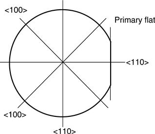
Single crystal silicon is the most widely used semiconductor material as a substrate material due to its excellent machinability, mechanical stability, and the potential to combine sensing elements and electronics on the same substrate. Circular wafers made of silicon are used as substrate in most MEMS sensors. The crystal orientation should be known before manufacturing, since silicon has orientation-dependent properties such as piezoresistivity coefficients and etching rates. The common orientation is (100) where the numbers represent Miller indices (Madou, 2002). As an example, Fig. 10.1 shows a (100) wafer that has a primary flat side as an indication of < 110 > direction. When a piezoresistive element is placed on a (100) wafer, the orientation should be parallel to < 110 > direction if the piezoresistivity coefficients in that direction are intended to be utilized.
Since Smith (1954) demonstrated the piezoresistance properties of silicon, silicon has been used extensively in the sensor design. The fractional change in resistivity can be approximated in linear proportion to stress, as follows (Nathan and Baltes, 1999):
[10.1]
where π is the piezoresistivity coefficient and T is stress. The piezoresistivity coefficient depends on the crystal orientation of the silicon and the impurity concentration (i.e., dopant level and type). The piezoresistivity coefficients in the longitudinal and transverse directions are identified by the transformation of π from crystal orientation to the Cartesian coordinates (Kanda, 1982) as:
[10.2]
[10.3]
where l, m, and n are direction cosines and π11, π12, and π44 are the piezoresistivity coefficients depending on the silicon crystal orientation. Kanda (1982) shows the piezoresistivity coefficients of longitudinal and transverse directions graphically for p-type and n-type doped silicon substrates. The highest coefficients in longitudinal and transverse directions for (100) plane n-type wafer are achieved in the crystallography direction of < 100 > .
The impurities, n-type or p-type, can be introduced into single crystal silicon using diffusion or ion implantation techniques. While ion implantation controls the amount of impurities more accurately, it is an expensive process as compared to the diffusion technique. If the impurity concentration is increased, the piezoresistivity coefficients decrease; however, their temperature dependence decreases as well. Kanda (1982) demonstrated the piezoresistance factor as a function of impurity concentration and temperature. During the design of piezoresistive sensors, the dependence of temperature should be taken into consideration. A trade-off between sensitivity and temperature dependence should be considered for a specific application. Silicon, from a mechanical perspective, is a high strength, brittle material with low toughness, and its mechanical properties are given in Table 10.2.
b Polycrystalline silicon (polysilicon)
Polysilicon is the most common material for designing surface-micromachined devices. Polysilicon has material properties similar to single crystal silicon and can be doped via introducing impurities. Thin polysilicon layer to form microstructure can be deposited using low pressure chemical vapor deposition (LPCVP) technique. Polysilicon is made of grains that tend to increase in size with an increase in film thickness during the high temperature manufacturing steps (Zorman et al., 2006). Recrystallization of polysilicon increases the surface roughness, and affects mechanical and electrical properties. The manufacturing of polysilicon thick film may require chemical polishing to obtain smooth surfaces. Because of grain boundary effect and the limitations of deposition techniques, the thickness of structures made of polysilicon is typically limited to 2–5 μm.
c Silicon carbide
SiC is a semiconductor material with a band gap in the range of 2.3–3.4 eV, and excellent physical stability and mechanical properties with high melting point > 3000 °C. Therefore, it is an ideal material for high temperature applications and harsh environments (Mehregany and Zorman, 1999). SiC exhibits a one-dimensional polymorphism in various forms. Main SiC poly-types for device development are 4H-, 6H- and 3C-SiC. Micromachining SiC is more challenging than silicon. Plasma-based dry etching for SiC surface micromachining and laser ablation etching technique for SiC bulk micro-machining have been typically selected. 3C-SiC is the only polytype that can be deposited on silicon substrate, which makes it the dominant polytype for MEMS sensor applications (Jiang and Cheung, 2009). Various microma-chined structures can be designed using deposited polycrystalline 3C-SiC layers, such as lateral resonators and cantilevers (Fu et al., 2011; Wright and Horsfall, 2007).
d Metals
Metals are implemented as the principal conductors for power and signal transmission (e.g., aluminum) as well as structural elements (e.g., nickel). Metals are manufactured as thin films using deposition methods such as sputtering, or bulk materials using the electroplating method. To obtain a thick metal layer, a mold is applied in order to pattern an electroplated layer on the surface, as discussed under the LIGA method.
e Sacrificial layers
Sacrificial layers are required between substrate or insulator layer and the microstructure layer in order to release the deposited microstructure layer functioning as moving element. Silicon oxide (SiO2) is the most typical layer used in the surface micromachining method because it can be easily dissolved without affecting other layers such as polysilicon and silicon nitride. Good thermal matching of SiO2 makes it a good candidate as compared to aluminum.
f Insulators
Typical insulating layers include silicon dioxide, silicon nitride, and titanium nitride (Spearing, 2000). Silicon nitride has 1016 Ω-cm resistivity, high dielectric strength, and field breakdown limit of 107 V/m (Madou, 2002).
10.2.2 Micromachining methods
There are three main micromachining methods used to design and manufacture MEMS sensors for SHM including bulk micromachining, surface micromachining, and LIGA. Most of the processing steps are adapted from IC technology. Three main processes are deposition, lithography, and etching. Deposition can be achieved using oxidation, chemical vapor deposition, epitaxy, physical vapor deposition, diffusion, and ion implantation. Lithography methods to pattern the shapes are optical and electron diffusion. Etching methods are wet or dry etching. Figure 10.2 shows the process steps of three micromachining methods in order to create a freely moving microstructure layer. Each process step is explained below.
a. Bulk Micromachining: the microstructure geometry is featured by dry or wet etching of bulk three dimensional materials. Etching masks are used in order to remove selected areas for creating the design geometry. Increasing dopant concentration increases the etching rate due to the mobile carriers. Wet etching processes may increase the residual stress at films. Dry etching techniques include reactive ion etching (RIE) sputtering, ion milling, and plasma etching. Figure 10.2a shows a simple geometry design using bulk micromachining method. It is assumed that the process is started with a doped silicon substrate. Back-side etching (step 2) removes a section of substrate. Oxidation (step 3) creates an insulator layer to electrically disconnect the substrate and microstructure layer. Doped polysilicon can be deposited on the oxidized layer to be used as strain sensor.
b. Surface Micromachining: surface micromachined MEMS sensors are designed by the deposition, patterning, and etching of layers on the surface of a substrate, typically used in the complementary metal oxide semiconductor (CMOS) manufacturing. The processes can be used to fabricate standing and freely moving microstructure layers in a large two-dimensional design space. Figure 10.2b shows a simple geometric design using surface micromachining method. After depositing sacrificial layer (step 1), the layer is patterned and then etched (step 2) depending on the design geometry. The next step (step 3) is to deposit the microstructure layer and then pattern and etch it (step 4). Finally, the sacrificial layer is selectively removed (step 5) using wet etching technique in order to create a freely moving microstructure layer.
Thin film properties play an important role for the sensor characteristics. Due to the limitations of depositing techniques, the thickness of microstructure is limited to 2–5 μm. The drawbacks of the surface micromachining method include the property and thickness variability due to deposition, stiction of layers during release process (the contact of two parallel layers after the release of the freely moving microstructure layer), and thickness limitation. However, polysilicon has superior material properties and the process can be combined with the CMOS processes for on-chip electronics (e.g., pre-amplifiers, filters).
The release process may cause thin film residual stress after the sacrificial layer is removed to release the microstructure layer, which may modify the microstructure geometry (Romig et al., 2003). The residual stress can be controlled to some level by annealing the microstructure layer and designing it in a form that reduces the amount of residual stress. Plate VI (in the color section between pages 294 and 295) shows the elevation measurements taken from two different capacitive sensor geometries designed by Ozevin (2005). A non-contact optical profilometer can provide the dimensions of microstructures. Anchors for the diaphragm unit in a hexagonal shape were around the periphery of the polysilicon layer, while those for the piston unit in a square shape were inside. Anchor locations of the piston transducers reduced the deformation of polysilicon layer caused by the etching step.
c. LIGA: The LIGA process uses polymer mold created by lithography and electroplating metal into the mold cavities in order to create high aspect ratio structures. Structures with vertical side walls and aspect ratio of 100:1 can be manufactured using a highly collimated X-ray source (Beeby et al., 2004).
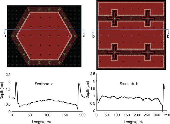
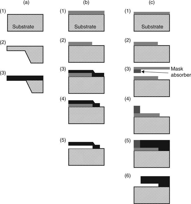
Figure 10.2c shows a simple geometry design with high aspect ratio design using LIGA. After depositing (step 1), patterning and etching (step 2) sacrificial layer, the layer is exposed to thick X-ray resist (step 3) with a mask and absorbers depending on the design pattern. X-ray resist is developed on the sacrificial layer (step 4); afterwards, a thick metal layer is electroplated (step 5). Finally, sacrificial layer is selectively etched and X-ray resist is stripped (step 6) in order to create a freely moving microstructure with high aspect ratio.
10.3 Sensor characteristics
The MEMS sensors for SHM can be built using the transduction principles of piezoresistivity, piezoelectricity, and capacitance. The size and manufacturing methods introduce several characteristics (i.e., stiction, squeeze film damping, and residual film stress) intrinsic to the MEMS sensors. This section describes the transduction principles and the MEMS sensor characteristics affected by the manufacturing methods.
10.3.1 Transduction principles
There are three main transduction principles used in the design of MEMS sensors for SHM: piezoresistivity, piezoelectricity, and capacitance. The piezoresistivity is based on the piezoresistive property of silicon demonstrated by Smith in 1954. The resistance Equation [10.4] and the relationship between resistance change (ΔR) and strain (Equation [10.5]) are:
[10.4]
[10.5]
where R is resistance, ρ is resistivity, L is length, A is cross-sectional area, ε is strain, and υ is Poisson ratio. The gage factor is defined as
[10.6]
For metals, the term Δρ/ρ is small; therefore, the gage factor is limited by Poisson’s ratio. A typical gage factor for metals is in the range of 1.4–2.0 (Barlian et al., 2009). In Section 10.2, the piezoresistivity coefficients with respect to resistivity change are provided. If the sensor is sensitive to longitudinal stress, Equation [10.6] can be simplified as
[10.7]
where E is Young’s Modulus and approximately equals 160 GPa for silicon. The piezoresistivity coefficient of n-doped silicon in the longitudinal direction and (100) plane of 11.7 ohm-cm resistivity is − 102.2E-11 Pa− 1 (Smith, 1954). The gage factor for n-doped silicon is theoretically about 165, which is significantly higher than metal foil gages. Polysilicon also exhibits piezoresistivity; however, the piezoresistivity coefficients are the average of all the directions.
The temperature dependence of piezoresistivity coefficients is significantly reduced with increasing impurity concentration N (i.e., reducing the resistivity), while the sensitivity of the sensor or its gage factor reduces simultaneously. The design requires an optimized point for the temperature dependence and the sensitivity. With unique microstructure geometry design, the sensor response can be amplified at the sensor level without need of an amplifier (Saboonchi and Ozevin, 2012). With the piezoresistivity transduction, strain, acceleration, and pressure can be measured.
The piezoelectric thin films can be deposited on silicon substrate with an insulator layer using various deposition techniques. Tadigadapa and Mateti (2009) summarize the challenges of piezoelectric property in MEMS sensors as high temperature need for piezoelectric deposition, incompatibility with CMOS, and morphology dependent piezoelectric properties. These challenges can be overcome with deposition techniques such as sputtering of aluminum nitride, chemical solution deposition of ferroelectric lead zirconate titanate (PZT) films, and patterning with plasma processes.
The piezoelectric equations for MEMS piezoelectric materials are similar to bulk type materials (Giurgiutiu, 2008):
[10.8]
[10.9]
where Sij and Tkl are the strain and stress, Ei and Dk are the electric field and electric displacement, the coefficient Sijkl represents stress per unit strain (compliance), and the coefficient gikl is the piezoelectric voltage coefficients. Piezoelectric coefficients vary depending on the thin film deposition technique. Tonisch et al. (2006) demonstrated the d33 coefficient of aluminum nitride (AlN) thin film as 5.1 pm/V. While piezoelectrics have a stable behavior for a wide temperature range, the applications of the piezoelectric MEMS sensors are so far limited (Muralt, 2008). Muralt et al. (2005) designed and manufactured 2 μm thick PZT film based MEMS ultrasonic sensor using solgel technique. The piezoelectric MEMS sensors can be designed as resonant or broadband. The resonant design requires dynamic factors (e.g., dynamic coupling factor) instead of static factors (Gaucher, 2002).
A capacitance is formed by two parallel conductors that can hold opposite charges. The capacitance of two parallel layers separated by air equals
[10.10]
where ε is the dielectric permittivity of material between plates, A is the overlap area between the top and bottom capacitive layers, and g is the gap between two capacitive layers. The capacitance change can occur due to the time variation of any of the variables, given in Equation [10.11] as:
[10.11]
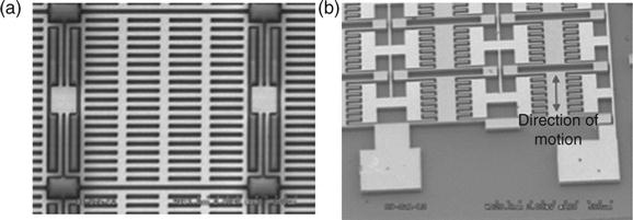
If a parallel plate capacitor is designed, the gap change is the conversion of mechanical signal to electrical signal. Figure 10.3a shows a group of parallel plate capacitors forming an AE sensor operating in out-of-plane direction manufactured using electroplating technique. If interdigital finger (i.e., comb drive) capacitors are designed, the area change or the gap change, Fig. 10.3b, is the cause of capacitance change. Major advantages of electrostatic sensing include fast response, which allows direct current (DC) level acceleration detection and simplicity. However, high power may be needed and parasitic capacitances may decrease signal-to-noise ratio.
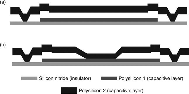
10.3.2 Stiction and collapse voltage
The stiction is the contact of two parallel conductive layers as illustrated in Fig. 10.4 on a capacitive sensor design constructed by two polysilicon layers on an insulator layer. Figure 10.4a shows the intended microstructure layer, and Fig. 10.4b shows the microstructure layer with the stiction. The stiction can occur either during the microfabrication or during the application of an electrostatic load. When removing the sacrificial layer with wet etching, the freely moving microstructure layer may come in contact with the substrate and remain there because of the surface tension created by wet etching. The stiction problem can be solved by several methods, such as designing a sufficiently rigid microstructure layer and immersing the microstructure into distilled water and alcohol immediately after the etching process (Madou, 2002). A dielectric layer deposited on the top surface of the bottom electrode can also prevent complete electrical contact and stiction while still allowing current flow due to low impedance path (Song et al., 2007).
Another cause of the stiction is the excessive application of electrostatic load. The freely moving microstructure layer has anchors on the substrate, which provide the mechanical stiffness. When an electrostatic load is applied across two microstructure layers, two layers pull toward each other. If the electrostatic load is applied excessively, the pulling force brings two layers into contact and leads to the stiction of two layers. For electrostatic designs, the maximum bias voltage Vbias that can be applied in the stable range and prevents stiction of the capacitive layers is referred to as the collapse voltage (Labadaum et al., 1998) and equals
[10.12]
10.3.3 Squeeze film damping
Squeeze film damping occurs in microstructures separated with a narrow band, and is caused by the air resistance under vibration of a freely moving microstructure layer due to air viscosity. The damping due to the fluid squeezing between two plates is modeled using Reynolds lubrication theory (Oppenheim et al., 2003a). Marrero et al. (2010) discuss the discrepancy between the actual measurement (c ~ 1/h where h is plate thickness) and the lubrication theory (c ~ 1/h3). The authors propose that the nonlinearity associated with Reynolds number is the explanation for this discrepancy. The squeeze film damping can be mitigated by increasing the gap between two capacitance layers, reducing the horizontal size of the freely moving microstructure layer, making holes in the freely moving microstructure layer to allow air to pass more readily, or by reducing the atmospheric pressure (Vinokur, 2003). Dienel et al. (2012) studied analytically and numerically the impact of vacuum pressure levels on the performance of MEMS sensors used in SHM to reduce the damping in resonant structures.
10.3.4 Thin film residual stress
Residual stress is induced on the microstructure layers due to mismatch in the thermal expansion coefficients of the deposited layers (e.g., polysilicon and silicon oxide), non-uniform plastic deformation, interstitial impurities, and the deposition process (Madou, 2002). The most significant effect of residual stress is gross deformation, such as curling of a cantilever, which can cause significant change in resonant frequency and buckling under compression. Plate VIa (see colour section between pages 294 and 295) shows an example of hexagon geometry and the thickness distribution along its length measured using a profilometer. The residual stress on thin film can alter stiffness, and consecutively the resonant frequency of the microstructure layer. Buckling is another consequence of thin film residual stress. Buckling is a frequent phenomenon in MEMS devices. Gaucher (2002) shows that if the dimensions of MEMS microstructure (width, thickness, and length) are decreased by a factor of 100, the Euler buckling load decreases by a factor of 104. The residual stress can be controlled to some level by annealing the microstructure layer. A second approach to control the residual stress is to design the microstructure layer in a form that reduces the amount of residual stress (Plate VIb).
10.3.5 Packaging
MEMS packaging is one of the critical barriers of MEMS progress in SHM for long term reliable usage, and it is still an active research field to design an effective and reliable packaging for MEMS sensors. The sensors need to be protected as well as exposed to environment for the transduction purpose, especially for corrosion sensing. For acceleration sensing, the sensing element and electronics can be sealed in a package while it still functions for inertia sensing. Li et al. (2013) showed that the sensitivity of a MEMS accelerometer depends on the thickness of the die adhesive and the die attachment process, and the density of the potting material. For AE sensing, the sensor surface should be in contact with the surface of the structure under health monitoring, in order to reduce the signal loss due to reflection in the layers. For a strain sensor, static strain requires complete removal of the sensor from the wafer for direct contact and the wiring should be on the mounted surface. Dynamic strain can be encapsulated in a sealed package. For a corrosion sensor, the sensing element may require direct contact with the environment, causing a reliability issue for long term implementation.
For any packaging, the die that carries the device (i.e., sensing elements and electronics) should be attached to the package as the first step, the connection pads on the device should be electrically connected to the pads in the package (metal, plastic, or ceramic as shown in Fig. 10.5) using the wire bonding method or flip-chip method as the second step, and then the package should be sealed with maximum protection that the sensing element will allow as the third step. The packaging steps can be done after or during (wafer level) the die manufacturing. The adhesive die attachment introduces stress on the sensing element, which affects the sensor behavior. Walwadkar and Cho (2006) showed that polyimide adhesive introduces less stress on the silicon die. Three failure mechanisms of protecting the MEMS device using capping are cavity deflection, cap fracture under impact, or drop and moisture penetration from sealant location, which detrimentally affect the hermetic bonding (Van Driel et al., 2007). Vacuum packaging usually fails due to leakage and outgassing (Chao, 2005). Mohammed et al. (2011) proposed a packaging scheme for the MEMS strain sensor, utilizing flip-chip technology; however, the packaging stiffens the strain response, which decreases the sensitivity. All the failure modes for the selected package method should be investigated deeply before implementing the sensor for long term SHM.

10.4 MEMS sensors for SHM
This section presents the prevailing sensors and sensing methods implemented for the SHM methods. The sensors include accelerometer, AE, strain, corrosion, and ultrasonic sensors. The sensors can be designed using a variety of transduction principles such as piezoresistivity, piezoelectricity, and capacitance. The MEMS sensors are described based on their transduction principles, and their advantages and challenges for the SHM applications are presented.
10.4.1 Accelerometer
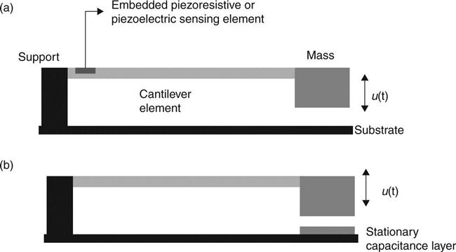
MEMS-based accelerometers can be designed using the transduction principles of piezoresistivity, piezoelectricity, and capacitance. The sensing elements can be designed for measuring multi-axis accelerations in linear and angular directions (i.e., gyroscopes). The frequency spectrum and bandwidth are controlled by mass and spring geometries. Figure 10.6 shows the schematic model of a cantilever accelerometer design, where the geometry for piezoelectric and piezoresistive types is similar. For capacitive transduction, a stationary layer is needed to form the capacitance and the gap or area change of the capacitance can be the transduction principle.
Two main challenges of MEMS accelerometers are to design a sensor operating below 1 Hz, which is a typical vibration frequency of long span bridges, and to sense low-level ambient vibrations (Jo et al., 2012). Piezoresistive sensors have DC response; however, n- or p-doped silicon used as piezoresistive material has a piezoresistive coefficient depending on temperature, as discussed in Section 10.3.1. Piezoelectric sensors have fast response and are difficult to design below 1 Hz. Capacitive sensors have DC response; however, due to parasitic capacitances, as discussed in Section 10.3.1, their sensitivity is low. The selection of transduction principle for MEMS accelerometer design depends on the specifications of an SHM application. There are numerous applications that integrate MEMS accelerometers with wireless units for monitoring damage in structures (Lynch and Loh, 2006), which are discussed under Section 10.5. Another challenge is the control of damping. For thin films, squeeze film damping controls the signal decay and varies with the deflected geometry and frequency. Therefore, damping is not constant for MEMS sensors unless they operate in vacuum.
The piezoresistive accelerometers are made of proof mass and spring elements, and the piezoresistive elements are deposited on spring elements, where they convert the acceleration induced strain into voltage when they are connected to a strain gage bridge. As discussed in Section 10.3.1, the orientations of piezoresistive elements control the sensitivity value and direction.
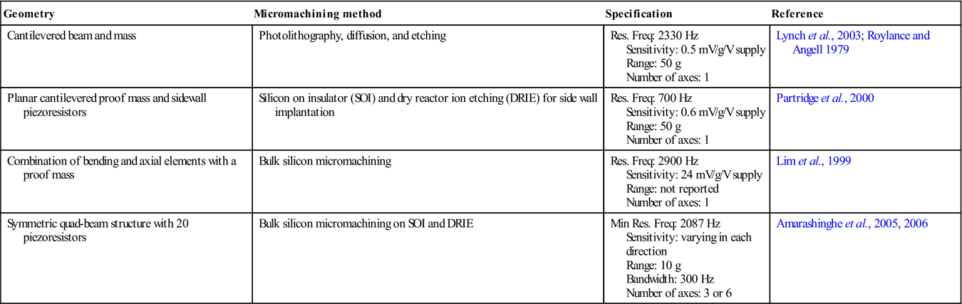
Roylance and Angell (1979) developed the first silicon-based accelerometer operating in out-of-plane direction with a mass structure and a cantilever beam that has piezoresistive elements. The weight of the MEMS accelerometer is less than 0.02 g, which has a large bandwidth and sensitivity. The sensitivity direction can be controlled using spring stiffness values (Chen et al., 1997; Partridge et al., 2000). Table 10.3 shows examples of piezoresistive MEMS accelerometers in the literature with their geometries, micromachining methods, and specifications. With unique microstructure geometry and flexibility of micromachining methods, novel, high sensitivity, wide bandwidth MEMS accelerometers can be designed and manufactured in a small package.
Table 10.3
Examples of piezoresistive MEMS accelerometers in the literature
| Geometry | Micromachining method | Specification | Reference |
| Cantilevered beam and mass | Photolithography, diffusion, and etching | Res. Freq: 2330 Hz Sensitivity: 0.5 mV/g/V supply Range: 50 g Number of axes: 1 |
Lynch et al., 2003; Roylance and Angell 1979 |
| Planar cantilevered proof mass and sidewall piezoresistors | Silicon on insulator (SOI) and dry reactor ion etching (DRIE) for side wall implantation | Res. Freq: 700 Hz Sensitivity: 0.6 mV/g/V supply Range: 50 g Number of axes: 1 |
Partridge et al., 2000 |
| Combination of bending and axial elements with a proof mass | Bulk silicon micromachining | Res. Freq: 2900 Hz Sensitivity: 24 mV/g/V supply Range: not reported Number of axes: 1 |
Lim et al., 1999 |
| Symmetric quad-beam structure with 20 piezoresistors | Bulk silicon micromachining on SOI and DRIE | Min Res. Freq: 2087 Hz Sensitivity: varying in each direction Range: 10 g Bandwidth: 300 Hz Number of axes: 3 or 6 |
Amarashinghe et al., 2005, 2006 |
The steady-state stress on a piezoelectric material decreases rapidly due to loss mechanisms in piezoelectric elements, which cause charge leakage. Therefore, piezoelectric sensors are designed for transient-response sensors (Tadigadapa and Mateti, 2009). Typical applications are in machine monitoring and the automobile industry. Similar to piezoresistive accelerometer sensor design is made of spring and mass. The sensing element, as piezoelectric film, is deposited on the spring to detect the acceleration induced strain (Hindriches et al., 2010). The common sensing direction for piezoelectric elements is d31 (Hindriches et al., 2010; Wang et al., 2002). Yu et al. (2003) designed an accelerometer using interdigitated electrodes, which utilizes d31 and d33 piezoelectric coefficients for better sensitivity. The MEMS piezoelectric accelerometers can be combined with commercially available wireless electronics (Kok and Furlong, 2005).
10.4.2 Acoustic emission sensor
AE are transient stress waves released within a material due to sudden stress–strain change caused by newly formed damage surfaces. The passive nature of the AE method requires sensors with high sensitivity and low noise level. The other sensor requirement is that the sensor surface area should be smaller than the smallest wavelength of the excitation signal to prevent the aperture effect. Typical frequency range used in civil structures is 60–400 kHz.
The AE sensors can be resonant or broadband types. The design of a broadband AE sensor is achieved by keeping the damping of the sensor high, which provides the fast damped response of the sensor causing a reduction in the amplitude of the output signal. Typical AE sensors are made of piezoelectric ceramics. However, it is not possible to design low frequency miniature AE sensors using conventional piezoelectric bulk ceramics.
There are three types of MEMS AE sensors designed in the literature: capacitive, piezoelectric, and optical. Ozevin et al. (2006) designed and characterized the first capacitive AE sensors in the literature fabricated in the commercial three-layer polysilicon surface micromachining process (Multi-User-MEMS-Processes (MUMPs)). Each transducer is a parallel plate capacitor with one plate free to vibrate, thereby causing capacitance change which creates an output signal in the form of a current under bias voltage. While the sensors could detect the AE events due to crack development in weld metal, their sensitivities are about fifty times less than conventional piezoelectric AE sensors (Ozevin et al., 2006). The current output i(t) in a capacitive transducer for a solid coupled system excited by x(t) is (Ozevin, 2005):
[10.13]
The squeeze film damping of thin films influenced the dynamic response x(t) of the microstructure. Harris et al. (2011) designed an improved capacitive AE sensor for out-of-plane sensing using the open-grill approach to reduce squeeze film damping. They also designed a comb drive sensor for in-plane sensing; however, the design limitations of the micromachining process used in this research causes coupling of in-plane and out-of-plane sensing for comb drive design. Saboonchi and Ozevin (2013a) designed and manufactured capacitive type MEMS AE sensors using an electroplating technique. The sensors are manufactured by MetalMUMPs process, which allows higher aspect ratio geometry than surface micromachined sensors. The MEMS AE sensors in this study operate at atmospheric pressure, and have signal-to-noise ratio comparable to bulk type piezoelectric sensors at their resonant frequencies.
Feng and Tsai (2010) designed a piezoelectric AE sensor made of multilayer polyvinylidene fluoride (PVDF) using a micro-embossing fabrication technique. The sensor has an operational frequency range of 10 kHz–1.4 MHz. Schoess and Zook (1998) implemented a resonant micro-beam as an AE sensor. Under an excitation signal caused by propagating elastic waves, a micro-beam made from polysilicon vibrates, which is converted to mechanical signal using a focused laser system. The MEMS design approach developed in this study can be combined with fiber optic systems for a compact AE sensor design.
10.4.3 Strain sensor
There are several recent strain sensor designs in the literature using MEMS. However, the performance of MEMS strain sensors is currently limited to laboratory scale experiments. Mohammed et al. (2011) designed the MEMS strain sensor with lower dopant concentration while the geometry amplifies the strain value. Direct measurement of strain requires robust bonding of the strain gage directly on the measurement surface. Kim et al. (2010) designed a thin polysilicon gage that can be separated from the wafer for direct attachment to the surface. However, fragility can be an important issue for this process. Bahreyni et al. (2006) fabricated piezoresistive sensors using the standard MUMPs (Multi-User Polysilicon) process. The geometry is a twin-beam structure separated by air so that the total strain in the polysilicon layer is non-zero. Waterfall et al. (2008) demonstrated that the relationship between the bending strain and piezoresistivity of the polysilicon layer is nonlinear. The temperature dependence of the piezoresistivity coefficients of the silicon and decoupling the sensor from wafer, are two challenges that need to be addressed for the use of MEMS strain sensors to replace conventional foil gages.
Adhesive bonding degradation of strain sensors with time and environmental factors limits the lifetime of the sensors for long term monitoring. Sosnowchik et al. (2012) developed an alternative bonding method based on the eutectic bonding of MEMS strain sensor to steel using an induction heating system.
10.4.4 Corrosion sensor
Corrosion can be monitored indirectly using parameters such as humidity, temperature or directly using corrosion sensor. Humidity can be measured using various transduction principles of MEMS such as the capacitance change (i.e., dielectric constant change in direct proportion to humidity) and resistivity change due to humidity. MEMS temperature sensors are commercially available analog devices. Norris et al. (2006) demonstrated the embedded MEMS temperature and moisture sensors into concrete. The sensors were made of silicon cantilever with embedded strain gages for piezoresistivity transduction in proportion to temperature and moisture.
For direct measurement of corrosion, the sensor material should be the same as the material being monitored for corrosion. Hautefeuille et al. (2009) designed a MEMS corrosion sensor as part of a wireless sensor network mote using a 0.5 μm thick metal layer made of aluminum and 1% silicon as the active layer of corrosion sensor. Electrical resistance change of metal layer, due to corrosion development, is the transduction principle for corrosion monitoring. There are not many design examples for the MEMS corrosion sensor in the literature.
10.4.5 Ultrasonic sensor
The application of MEMS technology to ultrasonic transducers has been studied since 1998. Khuri-Yakub et al. (1998) and Jin et al. (1998) presented a capacitive transducer fabricated using a silicon micromachining method. The sensor sensitivity was comparable to the piezoelectric sensor, and the sensor was evaluated in air-coupled and immersion applications. The advantage of the silicon micromachined capacitive transducer, as compared to the piezoelectric transducer, is that the silicon has no acoustic mismatch problem for the ultrasonic testing at air-coupled applications. The acoustic mismatch between air and piezoelectric material results in the ultrasonic sensor having either narrow bandwidth or poor efficiency, along with the difficulty of creating the proper impedance matching layers. In addition, the capacitive MEMS sensor can be used in high temperatures, whereas the behavior of the piezoelectric sensor is modified above the Curie temperature. The researchers reported several innovative processes in the capacitive MEMS sensor fabrication to optimize sensor performance (Jin et al., 1999). Bashford et al. (1998) also showed the superiority of water-coupled micromachined ultrasonic capacitive sensors over piezoelectric sensors.
Oppenheim et al. (2003a, 2003b) studied a solid coupled capacitive diaphragm MEMS sensor fabricated using the MUMPs. The geometry is similar to Plate VIa (see colour section between pages 294 and 295). The capacitance of a single diaphragm unit is insufficient to function as a sensor; therefore, 180 diaphragm units are placed in parallel to form a single sensor (Jain, 2002). An electromechanical model of capacitive MEMS sensors is described by Oppenheim et al. (2003a) and Ladabaum et al. (1998).
10.5 Application examples
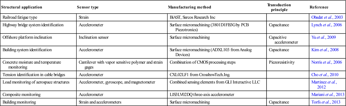
MEMS sensors are continuously implemented in certain applications, such as in the automobile industry. However, in the field of civil structures, they are not sufficiently established to be implemented for continuous monitoring because of the challenges of power source and durability. The long term technical challenges of MEMS are discussed in Section 10.6. Additionally, packaging and integration with electronics are another two barriers to the extensive use of MEMS sensors in SHM (Glaser et al., 2007).
Table 10.4 shows some application examples of MEMS sensors in the literature. The applications range from system identifications of buildings and bridges to concrete monitoring for corrosion. Some of these applications are limited to laboratory scale demonstrations. The most mature MEMS sensor used in civil structures is the MEMS accelerometer for system identification. Various design options are described in Section 10.3. Ramos et al. (2010) summarize the evolution of wireless accelerometer designs, including the MEMS accelerometer, in the field of SHM. However, there are limited numbers of field validations demonstrating the long term durability of the sensors. Chung et al. (2004) demonstrated the integration of MEMS accelerometers manufactured by Analog Devices (ADXL 202E) and Silicon Design (SD1221) with a wireless system for monitoring a pedestrian bridge. While the MEMS sensors have lower signal-to-noise ratio, they detected the fundamental frequencies of the bridge as compared to conventional cabled sensor. However, the pedestrian bridge was a short term demonstration.
Table 10.4
Examples of MEMS sensors in monitoring civil structures
| Structural application | Sensor type | Manufacturing method | Transduction principle | Reference |
| Railroad fatigue type | Strain | BiAST, Sarcos Research Inc | Obadat et al., 2003 | |
| Highway bridge system identification | Accelerometer | Surface micromachining (3801D1FB3G by PCB Piezotronics) | Capacitance | Lynch et al., 2006 |
| Offshore platform inclination | Inclination sensor | Surface micromachining | Capacitive accelerometer | Yu et al., 2009 |
| Building system identification | Accelerometer | Surface micromachining (ADXL103 from Analog Devices) | Capacitance | Kim et al., 2008 |
| Concrete moisture and temperature monitoring | Cantilever with vapor sensitive polymer and strain gages | Combination of CMOS processing steps | Piezoresistivity | Norris et al., 2006 |
| Tension identification in cable bridges | Accelerometer | CXL02LF1 from CrossbowTech.Ing. | Cho et al., 2010 | |
| Load monitoring of aerospace structures | Accelerometer, gyroscope, and magnetometer | Combined sensing elements from GLI Interactive LLC | Martinez et al., 2012 | |
| Composite monitoring | Accelerometer | LIS3LV02DQ three-axis accelerometer | Mariani et al., 2013 | |
| Building monitoring | Strain and accelerometers | Surface micromachining | Capacitance | Torfs et al., 2013 |
10.6 Long term technical challenges
There has been a remarkable progress in MEMS sensors since the 1980s. However, the challenges of long term durability and processing effects are still present for the implementation of the MEMS sensors in civil structures for continuous monitoring. Understanding the failure mechanisms of MEMS sensors packaged using sealant or caps is a difficult task, as removing the protective layer nondestructively is not possible (Walraven, 2005). Huang et al. (2012) lists typical failure modes for MEMS sensors, such as mechanical fracture, stiction, charge accumulation, wear, creep, fatigue, electrical degradation, and environmental contamination. Tanner (2009) discusses the reliability of MEMS components based on the groups as (1) no moving parts, (2) moving parts, no rubbing or impacting surfaces, (3) moving parts with impacting surfaces, and (4) moving parts with impacting and rubbing surfaces. The groups 3 and 4 include mirrors and switches where impacting and rubbing cause surface wear. The MEMS sensors used in SHM have components in groups 1 and 2. Moving parts can have fatigue, fracture, and creep depending on environmental and loading conditions, and stiction depending on the level of deformation or the applied voltage. Humidity and temperature can damage the sealant of the protective package causing outgassing for vacuum packaged sensors. The MEMS package and sensing element can also be damaged due to unintentional drop or shock vibration caused by thunder struck in highway bridges. The long term durability of the sensor should be evaluated based on the conditions of the specific application.
Repetitive cycling of silicon thin films, especially at their resonant frequencies (typically used to design an AE sensor) can cause fatigue. Silicon is a brittle material with low damage tolerance and fracture toughness (![]() as reported at Muhlstein et al., 2004). Bagdahn and Sharpe (2003) showed that the tensile strength of thin polycrystalline silicon film decreases about 35% after 109 cycles. Such decrease in strength and stiffness change may not be acceptable for sensor designs for long term usage. Swadener and Nastasi (2003) showed that the Ne implantation to boron-doped silicon increases the fracture toughness of silicon. Such an increase can be beneficial for long term durability of resonating parts of MEMS sensors.
as reported at Muhlstein et al., 2004). Bagdahn and Sharpe (2003) showed that the tensile strength of thin polycrystalline silicon film decreases about 35% after 109 cycles. Such decrease in strength and stiffness change may not be acceptable for sensor designs for long term usage. Swadener and Nastasi (2003) showed that the Ne implantation to boron-doped silicon increases the fracture toughness of silicon. Such an increase can be beneficial for long term durability of resonating parts of MEMS sensors.
As discussed earlier, the reliability of packaging influences the long term usage of MEMS sensors in civil structures. Wafer level packaging increases the durability of the sensor as compared to component level packaging, especially for the sensors, which require a vacuum environment such as inertia sensors (Gooch et al., 1999). Packaging influences the damage level for accidental drops (Ghisi et al., 2009).
10.7 Conclusion and future trends
MEMS provide diverse micromachining processes, including bulk, surface, and LIGA, which allow designing unique microstructures for sensing and actuating. There are a wide variety of sensor materials and manufacturing options that can be modified for sensing need and environmental conditions. The most common microstructure material used in SHM is silicon. The transduction mechanism can be piezoresistive, capacitive, or piezoelectric. As compared to macro-scale sensors, residual film stress and squeeze film damping are two issues related to MEMS that should be considered in the design process. The sensor design and the final packaging should be designed in order to prevent failure. While there has been a remarkable progress in MEMS sensors in laboratory scale demonstrations, packaging is still a barrier for long term implementation of MEMS sensors in civil structures.
The future trends of MEMS for SHM are grouped as novel sensor designs to increase the localized information about the structural condition, durability demonstration, electronics integration on the wafer level, and intelligent data acquisition.
a. Novel sensor design: the uncertainties in the SHM methods require data fusion in order to develop reliable prognostic models. The diversity of materials and manufacturing methods available in the MEMS field allow designing novel sensor fusion opportunities to be manufactured on the same wafer. Discrete sensor elements (e.g., AE, accelerometer) on the same device can open tremendous opportunities in SHM of civil structures (e.g., Martinez et al., 2012; Saboonchi and Ozevin, 2013b). Additionally, accelerometers with six degrees of freedom can be allocated in a miniaturized package. The additional localized information increases the interpretation of system behavior and change due to deterioration.
b. Durability demonstrations: MEMS implementation in the field is affected by unknown durability conditions for long term monitoring. The MEMS sensors need to be tested in the laboratory using accelerated test models, and their durability should be validated in the field using long term data acquisition (> 1 year).
c. Electronics integration: the electronics for signal conditioning and computing systems should be incorporated into the same package of sensing element in order to reduce the noise level and increase long term durability. Wireless integration of MEMS sensors with energy harvesting devices opens new opportunities for the applications that require mass, space, and power constraints. MEMS sensors should be integrated with CMOS digital circuit technology to reduce the power consumption and cost, and to increase efficiency (Tan et al., 2011).
d. Intelligent data acquisition: for intelligent data acquisition, RF MEMS switches can be integrated into the design as a trigger source in order to prevent the energy consumption and the record of unwanted information.