
22
HIGH-END SILICON PHOTODIODE INTEGRATED CIRCUITS
Optoelectronic integrated circuits (OEICs) [1–3] are used for very compact designs and low-cost application—for example, for optical storage systems such as CD-ROM, DVD, digital video recording, enhanced video disc (EVD), and Blu-ray Disc (BD) or for fiber receivers such as low-cost data comm receivers for plastic optical fibers (POFs). They are important because the inherent compactness of monolithic optical integrated circuits gives the following advantages: good immunity against electromagnetic interference (EMI) due to very short interconnects between photodetectors and amplifiers, reduced chip area because of elimination of bondpads, improved reliability due to the elimination of bondpads and bond wires, cheaper mass production compared to discrete-, wire-bonded-, or some hybrid integrated circuits, and a larger −3-dB bandwidth compared to discrete- or wire-bonded circuits, because of the avoidance of parasitic bondpad capacitances.
Inexpensive optical receivers with top performance are in great demand. Especially the low-cost requirement permanently drives and pushes silicon photodiode integrated circuts (PDICs) instead of expensive III/V semiconductor receivers. For high data rates of more than 10 Gbit/s, III/V receivers have a better performance and it is useful to accept their high costs; but for lower data rates up to about 10 Gbit/s, silicon PDICs with their lower production costs combined with the advanced circuit design of silicon chips are more attractive for mass market and are true competitors.
This chapter concerns silicon photodiode integrated circuits (PDICs), where the focus is on silica fiber receivers and on low-cost data comm receivers for plastic optical fiber (POF) applications. After a short explanation of some basics and a typical integrated pin-photodiode, circuit concepts of fiber receivers with data rates up to 11 Gbit/s as well as a parallel optical receiver for data rates of 100 + Gbit/s and a multilevel receiver are described.
22.1 OPTICAL ABSORPTION OF IMPORTANT SEMICONDUCTOR MATERIALS
Light can be described by a wave formalism and, due to the work of Max Planck and Albert Einstein, also by a quantum-mechanical light particle (photon) formalism. A photon does not possess a quiescent mass and can be characterized by its frequency f and by its wavelength λ as well as by its energy E [see Eqs. (22.1) and (22.2)], where c is the speed of light in a medium, c0 is the speed of light in vacuum, n is the index of refraction of the medium, f the frequency, λ is the wavelength in the medium, λ0 is the vacuum wavelength, and h is Planck’s constant.
In semiconductors the bandgap energy Eg, which is the distance between the conduction band and the valence band, determines the boundary wavelength of light, which can be absorbed by the material. Silicon has a bandgap energy of Eg = 1.1 eV and a boundary wavelength λc according to Eq. (22.3) can be stated.
When the photon energy E is larger than the bandgap energy Eg, this energy can be transferred to an electron in the valence band of a semiconductor. These photons are absorbed, electron–hole pairs are generated, and thus a photocurrent is able to flow. Only light with shorter wavelengths than λc can be detected, because then absorption increases rapidly according to the so-called fundamental absorption. For wavelengths longer than λc the semiconductor is transparent. For silicon, λc = 1110 nm.
The most
important optical constant for photodetectors is the optical absorption coefficient
α (see Figure 22.1) or the reciprocal value 1/α, which is the 1/e-penetration depth according to Lambert–Beer’s law in Eq. (22.4),
where I0 is the light intensity at y = 0+ and I(y) is the light intensity in a depth y below the surface of the semiconductor (see Figure 22.2). The
absorption coefficient strongly depends on the wavelength of the light. As mentioned
before, the absorption coefficient gets large for wavelengths shorter than λc. At λc, the steepness of the onset of absorption is large for
direct band–band transition like in GaAs (![]() at 300 K), in InP (
at 300 K), in InP (![]() at 300 K), or in Ge (
at 300 K), or in Ge (![]() at 300 K) and small for indirect band–band transition as in Si
(
at 300 K) and small for indirect band–band transition as in Si
(![]() at 300 K) or in Ge (
at 300 K) or in Ge (![]() at 300 K). In Figure 22.1 the
optical absorption coefficients α for Si, Ge, and
several SiGe alloys versus the wavelength are depicted. Due to the fact that silicon
is an indirect semiconductor, the absorption coefficient in the visible (≈ 400–780
nm) and near-infrared spectrum (780–850 nm) is one or two orders of magnitude lower
than that of the semiconductor Ge, where its direct bandgap is only a little bit
larger than its indirect bandgap. Although it is worthwhile to investigate silicon
photodiode integrated circuits because it is the economically most important
semiconductor. Equation (22.4) is multiplied at both sides with the
cross-section area A of light incidence to get the
optical power [Eq. (22.5)]. In Figure 22.2 the
decay of the optical power in the semiconductor with considering reflection of the
incoming optical power Popt = hfΦA (hf is the energy of a
photon and Φ is the number of photons incident per time
interval on an area A) according to Eq. (22.5)
is shown.
at 300 K). In Figure 22.1 the
optical absorption coefficients α for Si, Ge, and
several SiGe alloys versus the wavelength are depicted. Due to the fact that silicon
is an indirect semiconductor, the absorption coefficient in the visible (≈ 400–780
nm) and near-infrared spectrum (780–850 nm) is one or two orders of magnitude lower
than that of the semiconductor Ge, where its direct bandgap is only a little bit
larger than its indirect bandgap. Although it is worthwhile to investigate silicon
photodiode integrated circuits because it is the economically most important
semiconductor. Equation (22.4) is multiplied at both sides with the
cross-section area A of light incidence to get the
optical power [Eq. (22.5)]. In Figure 22.2 the
decay of the optical power in the semiconductor with considering reflection of the
incoming optical power Popt = hfΦA (hf is the energy of a
photon and Φ is the number of photons incident per time
interval on an area A) according to Eq. (22.5)
is shown.
Figure 22.1. Absorption coefficient a of silicon, germanium, and several SiGe alloys versus light wavelength λ.
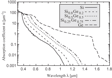
Figure 22.2. Decay of the optical power in the semiconductor (P0 = (1 − R)Popt) including reflection at the surface.
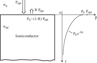
The reflection of the surface is caused by the different refraction indices between air (ns = 1 and the semiconductor (nSC ≈ 3.5 for SI). The reflectivity R depends on [see Eq. (22.6)] the index of refraction nSC and on the extinction coefficient κ of an absorbing medium, for which the dielectric function Φ = (nSC + jκ)2 is valid, where Φ is the complex permittivity of the medium and j the imaginary unit.
For calculating the absorption coefficient α, the extinction coefficient κ is sufficient [see Eq. (22.7)].
To avoid
reflection, the reflectivity R has to vanish. This can
be done for distinct frequencies by adding an anti-reflection coating (ARC) layer
between air and semiconductor with refractive index ![]() and with thickness dARC
= λ0/(4nARc).
and with thickness dARC
= λ0/(4nARc).
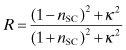
22.2 P–I–N PHOTODIODE
A principal
drawing of a p–i–n photodiode is shown in Figure 22.3. It
consists of a p–n junction
with an intrinsic (undoped) layer in between. To achieve a strong electric field
E in the intrinsic layer, the photodiode is reverse
biased with about 3–10 V [3]. The incoming photons (each with energy hf) create electron–hole pairs with a generation rate per
volume G(y) due to the
internal photoeffect with the condition that hf >
Eg. With the optical power P(y) [see Eq. (22.5)]
G(y) is equal to![]() . The result of this differential
equation is shown in Eq. (22.8) and in Figure 22.3.
. The result of this differential
equation is shown in Eq. (22.8) and in Figure 22.3.
Figure 22.3. Schmatic drawing of a p–i–n photodiode.
The generated electron–hole pairs are seperated in the intrinsic layer because of the high electic field E and an electrical current begins to flow. To characterize photodetectors with respect to their speed, the most important processes are carrier drift and minority carrier diffusion. In a typical semiconductor the carrier drift is a much faster process than the minority carrier diffusion. The influence of carrier drift and minority carrier diffusion in the time and frequency domain of the photocurrent is sketched in Figure 22.4. Besides junction capacitances, additional parasitic capacitances and series resistances are also important for calculation of a frequency response.
Figure 22.4. Schematic influence of carrier drift and minority carrier diffusion in the time and frequency domain of the photocurrent.
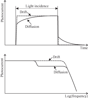
22.2.1 Carrier Drift
A photogenerated electron–hole pair in the intrinsic region is separated by the electric field. Due to this electric field in the reversed biased diode, the electron drifts toward region 2 (n+) while the hole drifts toward region 1 (p+) as shown in Figure 22.3. The drift velocity of electrons υn is proportional to the electric field E, υn = μnE, where μn is the mobility for electrons. The drift velocity of holes υp is proportional to E, υp = μpE, where the proportionality factor is the mobility of holes μp. The mobilities of electrons and holes depend, for example, on the temperature (higher temperature causes lower mobilities), on the doping concentration, and on the strength of the electric field. In silicon with low doping concentration (<10−16 cm−3), and electric field strengths of |E| < 2000 V/cm, we have typical values of mobilities of μn ≈ 1200 cm2/ Vs ≈ μn,0 and μp ≈ 450 cm2/Vs ≈ μp,0 at a temperature of T = 300 K, If the temperature is increased, the mobilities get smaller due to larger thermal vibration of lattice atoms and impurity atoms. When the doping concentration is higher the mobilities get smaller due to more scattering centers. The intrinsic region of a p–i–n photodiode is designed to have a low doping concentration and μn = μn,0 as well as μp = μp,0. If the field strength E is raised, the mobilities also degrade, as can be seen in Eqs. (22.9) and (22.10) [4].

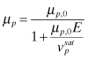
For values larger
than approximately 10,000 V/cm the electron drift velocity υn saturates to ![]() . On the contrary 25 the hole drift velocity υp saturates not until a value of about 100,000
V/cm. The values for the saturation velocities
. On the contrary 25 the hole drift velocity υp saturates not until a value of about 100,000
V/cm. The values for the saturation velocities ![]() and
and ![]() in cm/s are
nearly equal and can be computed from Eq. (22.11) [5], where T is the temperature in K.
in cm/s are
nearly equal and can be computed from Eq. (22.11) [5], where T is the temperature in K.
Ideally, to a p–i–n photodiode a sufficient reverse voltage is applied to get such a large electric field in the intrinsic zone that the drift velocities of electrons and holes saturate to υsat. To estimate rise and fall time (tr and tf, respectively) of the photocurrent, it is assumed that one of the charged particles of an electron–hole pair, which is generated at one of the borders of the intrinsic zone to the heavily doped areas, has to drift the whole length dI of the intrinsic zone and lasts the drift time tI. This marks the end of the rise time or the fall time, which therefore can be calculated as stated in Eq. (22.12).
Rise time and fall time limit the data rate, which can be received by the photodiode. Usually, drift times are much shorter than diffusion times, which are explained next.
22.2.2 Carrier Diffusion
As can be seen in Figure 22.4, minority carrier diffusion may degrade the bandwidth of a photodiode. Electron–hole pairs are generated not only in the intrinsic region of a pin photodiode, but also in the heavily doped p+ region 1 and in n+ region 2 (see Figure 22.3), where no electric field is present. In the p+ region the hole will be absorbed by the voltage source and the electron will first of all diffuse as minority carrier toward the intrinsic zone and then drift through this region and finally be absorbed by the voltage source, when it reaches region 2 and becomes a majority carrier. Diffusion of minority carriers in the p+ region is in most cases not critical due to the small thickness. On the other hand, a generated hole from the deep n+ region 2, which diffuses toward the intrinsic zone, has to overcome more distance and therefore needs more time. So critical for speed is usually minority carrier diffusion in the deep region 2. A characteristic value of what average distance a carrier is able to diffuse without recombination are the diffusion lengths Ln or Lp for electrons or holes, respectively, which can be seen in Eqs. (22.13) and (22.14) [2].
Dn and Dp are the diffusion coefficients for electrons and holes, respectively, and can be calculated via the Einstein relation [see Eqs. (22.13) and (22.14)], where kB is Boltzmann’s constant, q is the elementary charge, and UT is the thermal voltage. In silicon, Dn ≈ 35 cm2/s and Dp ≈ 12.5 cm2/s for low doping concentrations. These values reduce for high doping. The physical lifetime of a carrier (τn or τp for an electron or a hole, respectively) is due to dopants and unwanted impurities, which act as additional recombination centers in the semiconductor. These unwanted impurities are unavoidable because they are introduced in quite small but noticeable amounts in electronic devices during the fabrication process. The sizes of minority carrier lifetimes can reach several milliseconds in unprocessed grown silicon crystal. The fabrication process of integrated circuits or photodetectors can reduce the carrier lifetimes to the order of microseconds. Usually, p–i–n photodiodes are designed such that carrier drift is dominant over carrier diffusion, so usually diffusion times do not deteriorate the dynamical behavior. As mentioned above, the main influence of minority carrier diffusion to the photocurrent (see Figure 22.4) has its origin in the deep n+ region of the pin photodiode due to the larger thickness compared to the thin p+ region at the surface. For estimation of the time tdiff for which a hole diffuses in region 2 via a length dn (e.g., the thickness of region 2), an equation for a time-dependent sinusoidal electron density due to photogeneration in a p+ layer of a p–n photodiode was calculated in references 6 and 7, which is here adapted for an n+ region [see Eq. (22.15)].
In reference 7 the
equation for tdiff has been derived for a
time-dependent sinusoidal electron density due to photogeneration in the p+ layer from the electron diffusion equation.
There the time response of a low-pass filter with time constant ![]() was obtained. This time constant was
interpreted as the time that electrons need to diffuse to the space-charge region of
a p+n
junction.
was obtained. This time constant was
interpreted as the time that electrons need to diffuse to the space-charge region of
a p+n
junction.
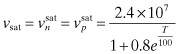
22.2.3 Quantum Efficiency and Responsivity
The total, external, or overall quantum efficiency η is defined as the number of photogenerated electron–hole pairs, which contribute to the photocurrent, divided by the number of incident photons [3]. This overall quantum efficiency can be determined when the photocurrent of a photodetector is measured for a known incident optical power. Because a fraction of the incident optical power Popt (see Figure 22.2) is reflected at the surface of a semiconductor, the external quantum efficiency η is the product of the optical quantum efficiency η0 = 1 − R and of the internal quantum efficiency ηi, which is a measure of how many electron–hole pairs contribute to the photocurrent [see Eq. (22.16)]. For example, generated electron–hole pairs may be lost due to recombination; or if there is a fast switching of optical power at high data rates, the slower minority carrier diffusion tail (see Figure 22.4) do not contribute to the photocurrent and the amplitude gets smaller.
The responsivity Rλ [see Eq. (22.17)] of a photodetector is a useful quantity for the development of photoreceiver circuits and especially of transimpedance amplifiers, because it is interesting to know how large the photocurrent is for a specified power of the incident light with a certain wavelength λ0. The responsivity is defined as the photocurrent iph divided by the incident optical power Popt.
In Eq. (22.17), q is the elementary charge, h is Planck’s constant, and c is the speed of light in a medium. Rλ depends on the wavelength; therefore the wavelength has to be mentioned if a responsivity value is given.
Figure 22.5 shows the reponsivity of real photodetectors versus the wavelength. The dashed line represents the maximum responsivity of an ideal photodetector with η = 1 (100%). The responsivity of real detectors is always lower due to partial reflection of the light at the semiconductor surface and due to partial recombination of photogenerated carriers in the semiconductor or at its surface.
Figure 22.5. Comparison of the responsivity of real photodetectors with an ideal photodetector with a quantum efficiency η = 1 (100%).
22.2.4 Implementation of an Integrated p–i–n Pliotodiode
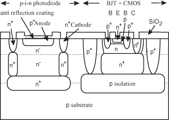
All integrated photodiode receivers, which are described here, are implemented in a 0.6-µm BiCMOS process with a nominal supply voltage of 5 V. The integrated p–i–n photodiode that was used for these receivers is similar to the design of the diode presented in reference 8, where the cross section is shown in Figure 22.6. Deep n+ plugs after low-doped n-epitaxial steps form the connection from the Si surface to the n+ buried-layer cathode. The electrical isolation between the n–p–n transistors and the n wells is formed by a p-isolation layer, which separates them. In reference 8 the reverse bias voltage was 3 V, and at 780-nm light a bandwidth of 300 MHz was achieved. To improve the speed of the photodiode with speeding up the carrier drift and as a consequence the bandwidth, the reverse bias voltage can be raised to values larger than the chip supply voltage of typically 5 V. This is because the n cathode is realized in a p-type substrate.
Figure 22.6. Integration of a p–i–n photodiode in a standard buried collector BiCMOS (bipolar + CMOS) technology [8] (BJT, bipolar-junction transistor).
22.2.5 Equivalent Circuit of a Photoreceiver
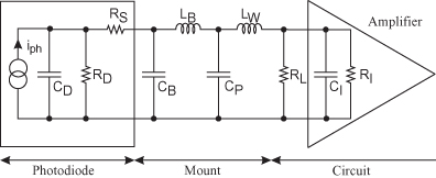
A small-signal equivalent circuit of the input of a photoreceiver considering parasitics due to mounting is shown in Figure 22.7. The current source iph represents the photocurrent, CD is the capacitance of the space-charge region with intrinsic region of a p–i–n photodiode. The parallel resistor RD models the reverse, leakage, or dark current. It is usually very large and can be neglected. The series resistor RS may not be neglected when the photocurrent flows through low-doped regions. But for a p–i–n photodiode with highly doped p and n regions it can be neglected when carrier drift dominates and the intrinsic zone is fully depleted. LB represents the inductance of the bondwire and CB is the capacitance of the bond wire. The stray capacitance of the detector package is considered in CP . The lead wires and the wiring on electronic boards introduce the additional inductance LW. For high frequencies, the inductances LB and LW become important. RL represents a load resistor; and CI and RI are the input capacitance and the input resistance, respectively of an amplifier. RI is important for amplifiers with a bipolar transistor input but can be neglected in most cases for JFET or MOS input transistors. It is clear that in a fully integrated photoreceiver the parasitics caused by mounting (CB, LB, CP, and LW) between the photodiode and the amplifier are saved, which enhances the overall bandwidth. This can be seen in Eq. (22.18), where the −3-dB bandwidth ∫3dB of the equivalent circuit of Figure 22.7 with the assumption that LB and LW can be neglected is depicted.
Figure 22.7. Small-signal equivalent input circuit of a photoreceiver.
22.2.6 Bit Error Ratio and Sensitivity
In the design of photodiode receivers,
many types of noise have to be considered—for example, either (a) electronic noise
caused by the photodiode and the transimpedance amplifier or (b) received optical
noise, which is overlaid to optical data signal. For more details on the different
noise sources here, see references 2 and 3. Here the overall noise will be
represented by an input-referred noise current with variance 〈![]() 〉 at the transimpedance amplifier
input, which can be obtained by integration of the spectral noise density 〈δi2(f )〉 over a
bandwidth B [see Eq. (22.19)], which defines the effective noise
bandwidth. Typically this bandwidth is between 0.5× to 0.75× of the bit rate [9].
〉 at the transimpedance amplifier
input, which can be obtained by integration of the spectral noise density 〈δi2(f )〉 over a
bandwidth B [see Eq. (22.19)], which defines the effective noise
bandwidth. Typically this bandwidth is between 0.5× to 0.75× of the bit rate [9].
It is assumed that the instant current values have a Gaussian distribution around the expected values 〈i0〉 and 〈i1〉, as can be seen in Figure 22.8. The resulting probability density function for a logical zero (p0(iph)) and a logical one (p1(iph)) are depicted in Eqs. (22.20) and (22.21).

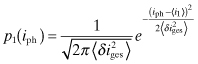
Figure 22.8.
Noisy non-return-to-zero (NRZ) input data signal (photocurrent iph) with noise statistics (probability
density functions p0(iph) and
p1(iph)) with variance
〈![]() of the noise). Here the
decision threshold Dt is the mean value
of 〈δi0〉 and 〈δi1〉 and the logical zeros and ones are assumed to be
equally distributed.
of the noise). Here the
decision threshold Dt is the mean value
of 〈δi0〉 and 〈δi1〉 and the logical zeros and ones are assumed to be
equally distributed.
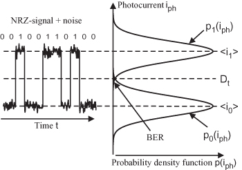
Furthermore, it is assumed that the logical zeros and the logical ones are equally distributed. Then the decision threshold for minimum decision failures is Dt = (〈i0〉 + 〈i1〉)/2, where for a current iph < Dt the detected signal is considered to be logical zero and for a current iph > Dt it is considered to be logical one. With these assumptions, the bit error ratio (BER) or the probability of a wrong decision is calculated by adding the probabilities that a zero is recognized by the receiver in the case that a one has been sent and the probability that a one is recognized in the case a zero has been sent. This probability is the black area in Figure 22.8 in the diagram with the probability density function. The probability of a false decision of the receiver is equal to the BER and can be calculated as depicted in Eq. (22.22).
The noise distance dn is depicted in Eq. (22.23).

For instance, BER = 10−9 holds at dn = 6 and BER = 1.3 × 10⁻¹² for dn = 7. The ratio r = 〈i0〉/〈i1〉 of the two photocurrent levels can be used to determine the mean optical power 〈P〉 of a binary signal with equally distributed logical zeros and ones, which is necessary to achieve a certain required BER [see Eq. (22.24)]. The BER is measured with the help of a fast oscilloscope which is able to catch eye-diagrams and amplitude statistics. Another possibility is to use a BER analyzer station, which compares the sent data stream with the received one and counts the errors. For the data stream for measurements on an oscilloscope or with an analyzer station a pseudo-random bit sequence with a certain length (e.g., 231 − 1) is used, which simulates random mean-free bit sequence, where the logical states are equally distributed.
Equation (22.24) was achieved by combining Dt = (〈i0〉) + 〈i1〉)/2 with Eq. (22.23) by using Dt = 〈P〉qη/hf. The quantity 〈P〉 in Eq. (22.24) is called sensitivity of the optical receiver and is usually expressed in dBm (10 × log(〈P〉/1 mW). It becomes lowest for r = 0—that is, 〈i0〉 = 0 or a vanishing optical power for a logical zero. As can be seen in Eq. (22.24), the sensitivity depends on the frequency f and therefore on the wavelength λ.
22.3 INTEGRATED PHOTODIODE RECEIVERS
22.3.1 An Integrated Silicon Photodiode Receiver for 5 Gbit/s with Voltage Up Converter
This integrated photodiode receiver uses a
similar p–i–n photodiode as shown in Figure 22.6
integrated in a 0.6-µm silicon BiCMOS process with a
nominal supply voltage of 5 V [10]. To improve speed and therefore the bandwidth of
the photodiode the reverse bias voltage of the diode was set to VPD = 11 V, a much larger voltage than the nominal supply
voltage. To generate such a voltage an additional voltage-up-converter was
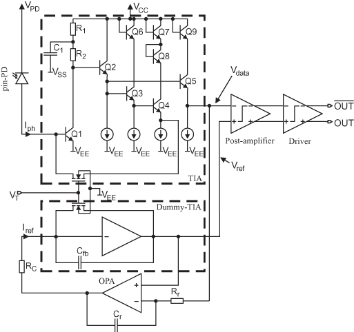
integrated. In Figure 22.9 the simplified schematic of the optical
receiver part is depicted. The p–i–n photodiode which
converts the incident light into an appropriate photocurrent iph in the integrated optical receiver part has a diameter of
50 µm. The TIA (transimpedance amplifier) converts this
current into a voltage Vdata with high bandwidth. A dummy TIA together
with a proportional-integral controller (OPA with Cr and Rr) creates an averaged voltage of
Vdata, which is the reference voltage Vref for the
following differential amplifier (post-amplifier). This controller defines also the
lower cutoff frequency, which is on the order of 50 kHz. The difference
Vdata − Vref is then amplified via the post-amplifier and
the driver, which is able to drive an off-chip 50 ![]() measurement system. The post-amplifier and the driver have also a symmetrical
limiting behavior to clip the logical voltage levels symmetrically in case of
overdrive to avoid large jitter. The MOSFETs used as active feedback resistors were
biased by an external bias voltage VT to have
the possibilitiy to adapt the receiver optimally to different data rates and
furthermore to enhance the dynamic range; for example, a high optical power at the
input requires a low feedback resistance. The value of the feedback resistance can
be adjusted with VT. The TIA itself consists
of an input common-emitter amplifier (transistor Q1),
which provides the voltage gain. The collector network was added to suppress
high-frequency supply noise and high-frequency feedback via supply lines, which
improves stability. On the other hand, at lower frequencies the gain is higher,
which introduces as a drawback a slight intersymbol interference and reduces the
sensitivity. Several emitter followers (Q2–Q5) are used for level shifting and impedance
transformation. To prevent breakdown of transistors (Q3–Q5), several diodes are added at the
collectors to reduce emitter–collector voltages.
measurement system. The post-amplifier and the driver have also a symmetrical
limiting behavior to clip the logical voltage levels symmetrically in case of
overdrive to avoid large jitter. The MOSFETs used as active feedback resistors were
biased by an external bias voltage VT to have
the possibilitiy to adapt the receiver optimally to different data rates and
furthermore to enhance the dynamic range; for example, a high optical power at the
input requires a low feedback resistance. The value of the feedback resistance can
be adjusted with VT. The TIA itself consists
of an input common-emitter amplifier (transistor Q1),
which provides the voltage gain. The collector network was added to suppress
high-frequency supply noise and high-frequency feedback via supply lines, which
improves stability. On the other hand, at lower frequencies the gain is higher,
which introduces as a drawback a slight intersymbol interference and reduces the
sensitivity. Several emitter followers (Q2–Q5) are used for level shifting and impedance
transformation. To prevent breakdown of transistors (Q3–Q5), several diodes are added at the
collectors to reduce emitter–collector voltages.
Figure 22.9. Simplified schematic of the optical receiver part.
The p–i–n photodiode voltage is generated by an additional on-chip voltage
up converter (VUC), which is shown in Figure 22.10. It consists of an oscillator, a
four-stage Dickson multiplier, and a low-pass filter to reduce the output voltage
ripple when biasing the photodiode. The oscillator operates with a symmetrically
built multivibrator, whereas the timing capacitance is formed by the pumping
network. The Dickson charge pump is also built symmetrically. The multivibrator
itself consists of two comparators (A and B), a flip flop, and an output stage to
drive the clock lines CLK and ![]() . Depending on the state of the flip
flop, it switches when either comparator A detects signals CLK failing below a threshold level or comparator B detects the same for
signal
. Depending on the state of the flip
flop, it switches when either comparator A detects signals CLK failing below a threshold level or comparator B detects the same for
signal ![]() . The threshold levels for
both comparators change with the state of the flip-flop, therefore forming a Schmitt
trigger behavior to prevent the circuit from unwanted oscillations. When only a low
photocurrent is flowing, the operating frequency is about 60 MHz. At higher currents
the stronger discharging for every cycle of the pumping capacitors leads to longer
time to fully recharge the pump capacitors and the frequency decreases. This is
because the charge pump capacitors are the load capacitances of the output stage of
the multivibrator, which determines the switching frequency. Therefore a stronger
discharging of the pumping capacitors occurs for every clock cycle with increasing
load current, which leads to a longer time to fully recharge the pump capacitors in
turn. The four-stage Dickson multiplier generates a voltage level VPUMP
= 11.9 V, which is filtered with transistor Q1, capacitor COUT,
and two resistors to determine voltage VPD.
The low-pass filter consists of an emitter–follower, whereby the base voltage is
filtered by a simple lead-lag filter with the corner frequencies of 1 MHz and 10
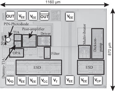
MHz. The microphotograph of the integrated photodiode receiver is shown in Figure 22.11. The
chip was fabricated in a modified 0.6µm BiCMOS
technology with a supply voltage of 5 V and with a transit frequency ft = 25 GHz of available n–p–n transistors. The total chip area was 1160 µm × 870 µm.
. The threshold levels for
both comparators change with the state of the flip-flop, therefore forming a Schmitt
trigger behavior to prevent the circuit from unwanted oscillations. When only a low
photocurrent is flowing, the operating frequency is about 60 MHz. At higher currents
the stronger discharging for every cycle of the pumping capacitors leads to longer
time to fully recharge the pump capacitors and the frequency decreases. This is
because the charge pump capacitors are the load capacitances of the output stage of
the multivibrator, which determines the switching frequency. Therefore a stronger
discharging of the pumping capacitors occurs for every clock cycle with increasing
load current, which leads to a longer time to fully recharge the pump capacitors in
turn. The four-stage Dickson multiplier generates a voltage level VPUMP
= 11.9 V, which is filtered with transistor Q1, capacitor COUT,
and two resistors to determine voltage VPD.
The low-pass filter consists of an emitter–follower, whereby the base voltage is
filtered by a simple lead-lag filter with the corner frequencies of 1 MHz and 10
MHz. The microphotograph of the integrated photodiode receiver is shown in Figure 22.11. The
chip was fabricated in a modified 0.6µm BiCMOS
technology with a supply voltage of 5 V and with a transit frequency ft = 25 GHz of available n–p–n transistors. The total chip area was 1160 µm × 870 µm.
Figure 22.10. Schematic of the voltage up-converter (VUC).
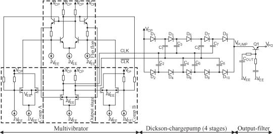
Figure 22.11. Microphotograph of the integrated photodiode receiver.
The
complete integrated photoreceiver consumes a current of 37 mA + 20 mA of the output
50-![]() driver, which results in a total power consumption of 285 mW (including 50-
driver, which results in a total power consumption of 285 mW (including 50-![]() driver). The receiver itself consumes 260 mW and the VUC 25 mW. The TIA itself
consumes 9 mW [10]. The overall transimpedance of the receiver ranges from 248 k
driver). The receiver itself consumes 260 mW and the VUC 25 mW. The TIA itself
consumes 9 mW [10]. The overall transimpedance of the receiver ranges from 248 k![]() to 58
k
to 58
k![]() .
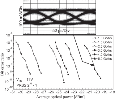
The measurement of the sensitivity and an eye diagram is shown in Figure 22.12. At a
wavelength of 660 nm at data rates of 2.5, 3, 4, and 5 Gbit/s the sensitivities (BER
= 10−9) were measured to be −24.9, −24.3, −22.9, and −20.5 dBm,
respectively. At a wavelength of 850 nm the sensitivity for a BER = 10−9
was −22.8 dBm at a data rate of 2.5 Gbit/s. This is because the responsivity of the
p–i–n photodiode was 0.36 A/W at a wavelength of 660
nm and 0.26 A/W at 850 m.
.
The measurement of the sensitivity and an eye diagram is shown in Figure 22.12. At a
wavelength of 660 nm at data rates of 2.5, 3, 4, and 5 Gbit/s the sensitivities (BER
= 10−9) were measured to be −24.9, −24.3, −22.9, and −20.5 dBm,
respectively. At a wavelength of 850 nm the sensitivity for a BER = 10−9
was −22.8 dBm at a data rate of 2.5 Gbit/s. This is because the responsivity of the
p–i–n photodiode was 0.36 A/W at a wavelength of 660
nm and 0.26 A/W at 850 m.
Figure 22.12. Bit error ratio versus the average optical input power at λ = 660 nm for different data rates. The eye diagram is for the case 5 Gbit/s, VT = 4 V and an average input power of −20.5 dBm.
22.3.2 An Integrated Silicon Optical Receiver for 850-nm Wavelength with a Data Rate Up to 11 Gbit/s
A high-speed all-integrated silicon optical receiver, which reaches data rates up to 11 Gbit/s, was designed in reference 11 in a 0.6-µm BiCMOS process with a nominal supply voltage of 5 V. The integrated p–i–n photodiode had a structure similar to the one shown in Figure 22.6. In a manner similar to that described in Section 22.3.1, the photodiode was biased with a voltage larger than the supply voltage. VPD = 17 V was chosen in reference 11. This enhances speed, and the −3 dB cutoff frequency was raised to 2.2 GHz at a wavelength of 850 nm.
To make data reception of more than about 4 GHz possible, the behavior of the diode was corrected with the help of an analog equalizer. Equalization of the photocurrent was successfully demonstrated with an n-well/p-substrate diode in reference 12, where the data rate of a standard optical receiver in a CMOS process was raised to 3 Gbit/s. The simplified schematic of the 11 Gbit/s photoreceiver with the detailed front end is shown in Figure 22.13.
Figure 22.13. Simplified schematic of the 11-Gbit/s photoreceiver.
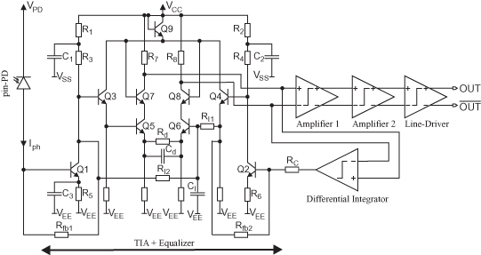
The
photocurrent Iph is converted into a voltage
with the help of the transimpedance amplifier (TIA) Q1, Q3, RI, R3, R5,
CI, C3, and Rfb1.
The TIA has a transimpedance of 500 ![]() . This voltage minus a reference voltage, which
is generated by a controlling circuit with differential integrator, is amplified
with a frequency-dependent characteristic proportional to the inverse characteristic
of the photodiode response. To achieve such an inverse characteristic, a cascoded
difference amplifier (Q5, Q6, Q7, Q8, R7, and R8) that has
frequency-dependent coupling elements is used. The drift time of the photodiode is
compensated with Rd and Cd, and the small diffusion part is compensated with
Cl, Rl1, and Rl2. After this equalizing amplifier the overall
transfer function has a nearly flat frequency response and linear phase. After the
TIA with the equalizer a three-stage limiting amplifier follows to improve the gain,
limit the signal amplitude, and drive a differential 100-
. This voltage minus a reference voltage, which
is generated by a controlling circuit with differential integrator, is amplified
with a frequency-dependent characteristic proportional to the inverse characteristic
of the photodiode response. To achieve such an inverse characteristic, a cascoded
difference amplifier (Q5, Q6, Q7, Q8, R7, and R8) that has
frequency-dependent coupling elements is used. The drift time of the photodiode is
compensated with Rd and Cd, and the small diffusion part is compensated with
Cl, Rl1, and Rl2. After this equalizing amplifier the overall
transfer function has a nearly flat frequency response and linear phase. After the
TIA with the equalizer a three-stage limiting amplifier follows to improve the gain,
limit the signal amplitude, and drive a differential 100-![]() load.
The controlling circuit generates together with the differential integrator and a
dummy TIA (Q2, Q4, R2, R4, R6, C2, and
Rjb2) the reference voltage
for the equalizing amplifier by injecting the average photocurrent Iavg into the dummy TIA via Rc. Thus, symmetrical clipping of the logical
voltage levels in case of optical overdrive is ensured. The controlling circuit
introduces a lower cutoff frequency of 30 kHz, eliminating the influence of
background light. The chip micrograph of the 11-Gbit/s integrated silicon optical
receiver is depicted in Figure 22.14. The p–i–n
photodiode has a diameter of 50 µm and matches to a
50-µm multimode fiber. The whole chip needs an area
of 870 µm × 700 µm, where
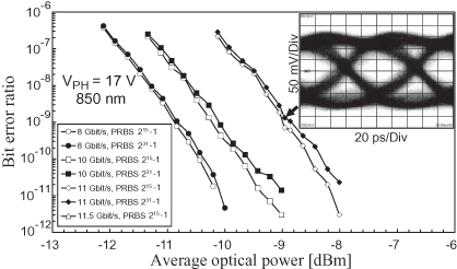
bond pads and supply blocking capacitors are included. The results of a BER
measurement to obtain the sensitivity of the optical receiver and an eye diagram at
11 Gbit/s, where an optical input power of −8.9 dBm is needed to achieve a BER of
10−9, can be seen in Figure 22.15. The analog upper −3-dB cutoff
frequency of the flat transfer function of the overall optical receiver chip is 7.7
GHz at a wavelength of 850 nm together with an overall transimpedance of 3 k
load.
The controlling circuit generates together with the differential integrator and a
dummy TIA (Q2, Q4, R2, R4, R6, C2, and
Rjb2) the reference voltage
for the equalizing amplifier by injecting the average photocurrent Iavg into the dummy TIA via Rc. Thus, symmetrical clipping of the logical
voltage levels in case of optical overdrive is ensured. The controlling circuit
introduces a lower cutoff frequency of 30 kHz, eliminating the influence of
background light. The chip micrograph of the 11-Gbit/s integrated silicon optical
receiver is depicted in Figure 22.14. The p–i–n
photodiode has a diameter of 50 µm and matches to a
50-µm multimode fiber. The whole chip needs an area
of 870 µm × 700 µm, where
bond pads and supply blocking capacitors are included. The results of a BER
measurement to obtain the sensitivity of the optical receiver and an eye diagram at
11 Gbit/s, where an optical input power of −8.9 dBm is needed to achieve a BER of
10−9, can be seen in Figure 22.15. The analog upper −3-dB cutoff
frequency of the flat transfer function of the overall optical receiver chip is 7.7
GHz at a wavelength of 850 nm together with an overall transimpedance of 3 k![]() . The
power consumption of the whole chip including the 100-
. The
power consumption of the whole chip including the 100- ![]() driver
is 310 mW at a supply voltage of 5 V [11]. It should be noted that the rather
moderate transitor transist frequency of about 25 GHz limited the performance at 11
Gbit/s.
driver
is 310 mW at a supply voltage of 5 V [11]. It should be noted that the rather
moderate transitor transist frequency of about 25 GHz limited the performance at 11
Gbit/s.
Figure 22.14. Chip micrograph of the complete integrated silicon optical receiver.
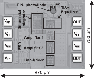
Figure 22.15. Bit error ratio versus average optical power at the input of the receiver. The eye diagram is for the case of 11-Gbit/s and −8.9- dBm optical input power.
22.3.3 Integrated Optical Silicon Receiver Front End for Multilevel Signaling
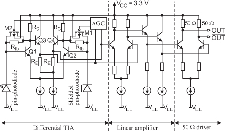
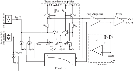
Reducing the analog bandwidth of a data stream with a distinct bit rate can be done by increasing the number of signal levels, where therefore the duration of a bit can be made longer. A common time-discrete signal, where the bit information is modulated into amplitude levels, is called an M-level pulse-amplitude-modulated signal (M-PAM). For an M amplitude-level scheme, the bandwidth is reduced by a factor of N under the assumption that the bit rate is held constant, where N is the number of bits per symbol: N = log2(M) [14]. On the other hand, breaking down an available voltage swing into a larger number of voltage levels reduces the voltage margin of the received symbol levels by a factor of 1/(M − 1). Therefore it is a higher challenge to design a multilevel receiver, because a better sensitivity and more receiver complexity compared to a usual two-level receiver for binary signals are needed. Due to the larger amount of voltage levels, also an automatic gain controller (AGC) has to be implemented in order to keep the different symbol levels equally spaced. A constant transimpedance or typical limiting post-amplifiers in a binary receiver will not be adequate in a multilevel receiver.
The schematic of
the front end of an integrated optical multilevel receiver is shown in Figure 22.16 [13].
The test chip was fabricated in a 0.6-µm BiCMOS process
and occupies a chip area of 1 mm2. The chip consumed 100 mW and was
designed for a single supply voltage of 3.3 V. The front end consists of an
integrated p–i–n photodiode, a transimpedance amplifier
(TIA), and a 50-![]() driver. A second identical p–i–n photodiode, which is shielded, is added to balance the
differential TIA. The p–i–n photodiode for optical
reception has a large diameter of 300 µm so that a
plastic optical fiber (POF) directly can be attached. The responsivity of the
photodiode is 0.48 A/W for λ = 660 nm. As shown in
Figure 22.16 the photocurrent, which is coming from the photodiode, is converted
into a voltage by a differential TIA. The AGC circuit decreases the transimpedance
of the TIA when the input optical power is increased to ensure that the output
voltage of the TIA is constant. The AGC measures the peak voltage at the output of
the differential TIA and keeps it constant for the highest level in the multilevel
signal by adjusting the transimpedance via transistors Ml and M2. When the optical
input power gets higher, the gate voltage at these transistors is reduced, thus
reducing the transimpedance. The lower cutoff frequency of the AGC circuit is 7.9
kHz [13].
driver. A second identical p–i–n photodiode, which is shielded, is added to balance the
differential TIA. The p–i–n photodiode for optical
reception has a large diameter of 300 µm so that a
plastic optical fiber (POF) directly can be attached. The responsivity of the
photodiode is 0.48 A/W for λ = 660 nm. As shown in
Figure 22.16 the photocurrent, which is coming from the photodiode, is converted
into a voltage by a differential TIA. The AGC circuit decreases the transimpedance
of the TIA when the input optical power is increased to ensure that the output
voltage of the TIA is constant. The AGC measures the peak voltage at the output of
the differential TIA and keeps it constant for the highest level in the multilevel
signal by adjusting the transimpedance via transistors Ml and M2. When the optical
input power gets higher, the gate voltage at these transistors is reduced, thus
reducing the transimpedance. The lower cutoff frequency of the AGC circuit is 7.9
kHz [13].
Figure 22.16. Schematic of the front end of an integrated optical multilevel receiver (4-PAM).
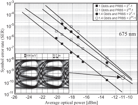
The measurement results of the chip are depicted in Figure 22.17. For a highest level of the input optical power of larger than 25 μW the output voltage is constant and equal to 750 mV. For M = 4 the logical voltage levels are equally spaced with 250 mV in between the output voltage range of 750 mV. Due to the low cutoff frequency of the AGC circuitry, a correct detection of the multilevel signal at constant threshold voltages is enabled. This optical receiver reaches sensitivities of −14.8 and −11.9 dBm for a data rate of 1 and 1.4 Gbit/s, respectively, at a wavelength of the received light at 675 nm with a SER of 10−9 for a pseudorandom bit sequence (PRBS) with a length of 27 − 1. With a PRBS of 23 − 1 and under the same conditions, sensitivities of −12.1 and −11.2 dBm for data rates of 1 and 1.4 Gbit/s were measured [13].
Figure 22.17. Measured 4-PAM symbol error rate (SER) versus average optical power at the input and eye diagram for 1.4-Gbit/s and −11-dBm optical input power.
22.3.4 36-Channel Integrated Silicon Optical Receiver with 3 Gbit/s per Channel
The growing use of the Internet and the demand for multi-Gbit/s I/O performance creates a need of 100+ Gbit/s data transmissions and therefore appropriate short-reach high-speed infrastructure for within high-end Telco and Datacom routers, switches, servers, and other chassis-to-chassis links. Solutions for low-cost high-speed optical receivers are also needed in consumer-electronic applications like HDTV interconnection standards (HDMI). Here a 36-channel integrated silicon optical receiver is described with a data rate of 3 Gbit/s per channel which results in an overall data rate of 108 Gbit/s [15]. The receiver chip was designed for a 0.6-µm BiCMOS technology with a supply voltage of 3.3 V and with integrated p–i–n photodiode with a responsivity of 0.33 A/W at 850 nm because the antireflection coating on the diode was optimized for 650 nm. However, if the ARC layer is optimized for 850 nm, the responsitivity will get better. The simplified schematic of one channel of the receiver with a detailed schematic of the differential TIA included is shown in Figure 22.18. The whole circuit is fully differential to achieve a good power supply rejection. This begins with a light-shielded p–i–n photodiode as reference, which has the same structure as the p–i–n photodiode for receiving optical data signals. The transimpedance amplifier (TIA) converts the photocurrent Ipd(t) to a signal voltage, which is further amplified by a post-amplifier and a final 50-Ω driver. An equalizer is implemented to correct the frequency-dependent response of the p–i–n photodiode by using steered current sources at the inputs of the TIA. An integrator with a lower cutoff frequency of 300 kHz is implemented to set the decision level via the reference input of the differential TIA. Additionally implemented but not shown in Figure 22.18 was a loss-of-power detector with adjustable threshold to detect whether one of the 36 channels receives not enough optical power.
Figure 22.18. Simplified schematic of one channel, which includes a detailed schematic of the differential TIA.
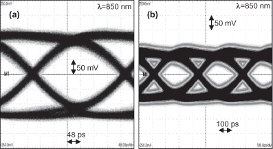
A chip photo of the 36-channel 108-Gbit/s integrated silicon optical receiver and a layout drawing of one channel (3 Gbit/s) are shown in Figure 22.19. The chip was fabricated in a 0.6-µm BiCMOS process with a supply voltage of 3.3 V. The diameter of a p–i–n photodiode is 90 µm and the photodiodes are arranged in a 250-µm raster. The whole chip consumes a power of 809 mW, which also includes an on-chip laser driver for a return channel and a loss-of-power detector. The crosstalk between two channels was measured to be below −40 dB. In Figure 22.20 the eye diagrams for one channel at 3 Gbit/s for an average optical input power of (a) −14 dBm and (b) −17.8 dBm for BER = 10−9 at a wavelength of 850 nm and with a laser extinction ratio of 6 using a PRBS 215 − 1. If the extinction ratio is assumed to be infinity (no optical power for the zero logical level) the sensitivity is calculated to −19.3 dBm for one channel at a data rate of 3 Gbit/s.
Figure 22.19. Photo of the 36-channel integrated silicon optical receiver and layout drawing of one channel.
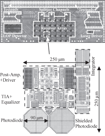
Figure 22.20. Eye diagrams at 3 Gbit/s (PRBS 215 − 1): (a) −14-dBm optical input power (b) −17.8-dBm optical input power.
22.4 CONCLUSION
The mighty capability of silicon PDICs was demonstrated in mature and reliable industrial silicon chip manufacturing technologies. The vertical integrated p–i–n photodiode realizes high bandwidth and high responsivity. Integrated voltage-up converters were shown to increase the data rate of silicon optical receivers up to more than 5 Gbit/s. Implementation of an equalizer in the TIA allowed even a data rate of 11 Gbit/s together with the vertical Si p–i–n photodiode. Another new approach—multimode data transmission—was successfully verified with a 4-PAM silicon PDIC. And finally a highly parallel high-speed PDIC up to a total data rate of 108 Gbit/s was introduced with a rather high sensitivity, rather low power consumption, and very good crosstalk behavior.
Altogether, silicon BiCMOS PDICs are very well appropriate for highspeed, high-sensitivity optical application-specific integrated circuits (OPTO-ASICs).
REFERENCES
1. H. Zimmermann, Integrated Silicon Optoelectronics, Springer, Berlin, 2000.
2. H. Zimmermann, Silicon Optoelectronic Integrated Circuits, Springer, Berlin, 2004.
3. K. Schneider and H. Zimmermann, Highly Sensitive Optical Receivers, Springer, Berlin, 2004.
4. D. M. Caughey and R. E. Thomas, Carrier mobilities in silicon empirically related to doping and field, Proc. IEEE, Vol. 55, pp. 2192–2193, 1967.
5. S. M. Sze, Physics of Semiconductor Devices, John Wiley & Sons, New York, 1981.
6. J. M. Senior, Optical Fiber Communications, Prentice-Hall, New York, 1992, p. 437.
7. G. Winstel and C. Weyrich, Optoelektronik II, Springer, Berlin, 1986, p. 76.
8. M. Yamamoto, M. Kubo, and K. Nakao, Si-OEIC with a built-in PIN-photodiode, IEEE Trans. Electron Devices, Vol. 42, No. 1, pp. 58–63, 1995.
9. K. J. Ebling, Integrated Optoelectronics, Springer, Berlin, 1993, p. 76.
10. R. Swoboda, J. Knorr, and H. Zimmermann, A 5-Gb/s OEIC with Voltage-Up-Converter, IEEE J. Solid-State Circuits, Vol. 40, No. 7, pp. 1521–1526, 2005.
11. R. Swoboda and H. Zimmermann, 11 Gb/s Monolithically integrated silicon optical receiver for 850 nm, in IEEE International Solid State Circuit Conference, February 2006, pp. 240–241.
12. S. Radovanovic, A.-J. Annema, and B. Nauta, 3 Gb/s Monolithically integrated photodiode and pre-amplifier in standard 0.18 µm CMOS, in IEEE International Solid State Circuit Conference, February 2004, pp. 472–473.
13. M. Atef, R. Swoboda, and H. Zimmermann, Optical receiver front-end for multilevel signalling, IET Electron. Lett. Vol. 45, No. 2, pp. 121–122, 2009.
14. S. Hranilovic and D. A. Johns, A multilevel modulation scheme for high-speed wireless infrared communications, in IEEE International Symposium on Circuits and Systems, Vol. 6, 1999, pp. 338–341.
15. R. Swoboda, M. Förtsch, and H. Zimmermann, 3 Gbps-per-channel highly-parallel silicon receiver OEIC, in 33rd European Conference on Optical Communication, September 2007, pp. 255–256.