
Chapter 2
Touch Sensing
Geoff Walker
Intel Corporation, Santa Clara, California
2.1 Introduction
This chapter is intended to provide a definitive reference on all touch technologies used in interactive displays. The objective of the chapter is to provide the reader with a substantial understanding of the operation, capabilities, advantages, disadvantages, limitations, and applications of 18 different types of touch technology. This understanding can be particularly helpful when touch is being combined with other input modalities in order to provide the user with more choices in how they can interact with a computer, as described in Chapters 1 and 9.
This chapter's scope is limited to touch technologies that operate by contact with a display screen, with the exception of stylus or finger “hover”, which generally takes place within 1 cm of the touch surface. Touch on opaque (non-display) surfaces, proximity sensing, and in-air (3D) gestures are therefore excluded from this discussion. This chapter also does not include any substantial information on touchscreen manufacturing.
In covering the wide array of touch technologies and system integration details, we focus more on the breadth of information on multiple technologies rather than the depth of technical information on any one technology. In this chapter (and throughout the touch industry) the terms “touchscreen” and “touch-panel” are synonymous; the former is more commonly used in the West, while latter is more commonly used in Asia. Both terms refer identically to a touch module consisting of a touch sensor, a touch controller, and a computer interface.
This chapter categorizes all touch technologies into six basic types, each with a number of sub-types (indicated in parentheses and totaling 18), as follows: capacitive (2), resistive (3), acoustic (3), optical (5), embedded (4), and other (1). “Embedded”, in this context, refers to touch capability that is fully integrated into a display by a display maker, as opposed to “discrete” touch capability which is added to a display by a touchscreen maker.
The touch industry is highly secretive; many of the 200+ companies in it are privately owned – even some very large ones. The result is that there are very few journal articles and no textbooks published by touch-technology inventors, developers or suppliers. That fact makes this chapter somewhat different from many of the other chapters in this book. In particular, the references are much broader – they include websites, magazine and newsletter articles, white papers, patents, conference presentations, press releases, user guides, and even blogs. Also because of the lack of journal articles and textbooks on touch technologies, the historical information in this chapter tends to focus somewhat more on when a touch technology was first commercialized than when it was invented.
2.2 Introduction to Touch Technologies
Displays, from CRTs to OLEDs, have long been used as information output devices. It is only recently that displays have reached widespread use as interactive input devices, mainly due to the addition or integration of touch-sensing capability into displays. From the first report of capacitive touchscreens by Johnson in 1965 [1], it took almost three decades until touchscreens were sufficiently developed to be widely used in business-owned products (i.e., in commercial applications) such as point-of-sale (POS) terminals and airport check-in terminals [2]. The first widely visible use of touchscreens in consumer-owned products (i.e., in consumer applications) was in personal digital assistants (PDAs) in the mid-1990s, the first of which was the Apple Newton in 1993, followed by Jeff Hawkins' more-famous Palm Pilot in 1997.
The event that launched the current trend of “touch everywhere” was the introduction of the Apple iPhone in 2007 [3]. Apple's implementation of a previously obscure but exceptionally easy-to-use touch technology (projected capacitive), combined with an immersive user interface, ignited a touchscreen growth-wave that is still climbing (Figures 2.1 and 2.2) [4]. Apple's choice of touch technology also changed the dynamics of the touchscreen industry, causing the formerly dominant analog-resistive technology to be replaced rapidly by projected-capacitive (p-cap) technology (Figure 2.3) [4].

Figure 2.1 Touch module shipments in billions of units, 2007–2012 actual and 2013–2017 forecast.
Source: Data from [4].
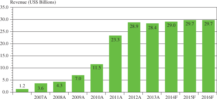
Figure 2.2 Touch module revenue in billions of US$, 2007–2013 actual and 2014–2017 forecast. Note: The author believes that the 103% increase between 2011 and 2012 is the result of a change in the market research analyst responsible for creating the report, rather than an actual change in market size of that magnitude.
Source: Data from [4].
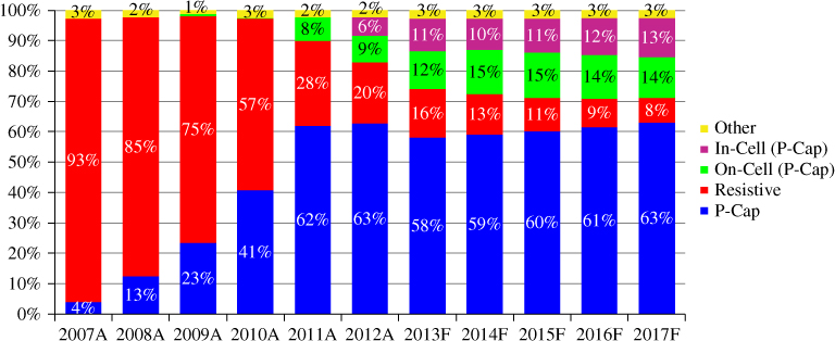
Figure 2.3 Touch technology by share of unit shipments, 2007–2012 actual and 2013–2017 forecast. Analog resistive was dominant with a 93% share in 2007; in 2012 that share had shrunk to 20%, with projected capacitive (in both discrete and embedded forms) taking 78%. DisplaySearch forecasts that in 2017 p-cap's share will increase to 90%, very close to the level of dominance that analog resistive had in 2007. Source: Data from [4].
Microsoft Windows 7, launched in July 2009, marked the initial appearance of touch in consumer all-in-one (AiO) home desktop computers. The following year Apple launched the iPad (April 2010), which was the first consumer device with 100% touch penetration (all tablets have touch capability, but not all mobile phones have touch capability). Microsoft Windows 8, launched in August 2012, marked the metamorphosis of Windows from a desktop-oriented operating system (OS) into a “touch-first” OS. As this book is being written in late 2013, the ramifications of that change are still reverberating throughout the personal computer (PC) and touchscreen industries.
2.2.1 Touchscreens
From the average user's perspective, a touchscreen is a computer display screen that can detect and respond to something touching it, such as a finger, a stylus, or the corner of a credit card. From a technology perspective, the display and whatever detects what is touching it are different electronic subsystems that must be treated separately. When they are combined, they are more properly called an “interactive display” or sometimes just a “touch display”.
In this chapter, the term “touchscreen” is used to describe just the electronic subsystem that detects the user's touch and translates that touch into information that a computer can understand and use. For the majority of today's products, this subsystem is supplied by a company that specializes in touchscreens (usually called a touch-module maker). The integration of the touchscreen and the display can be performed by the touch-module maker, by the display-maker, by a systems integrator, or by an OEM/ODM device-maker (for consumer electronic devices, an Original Equipment Manufacturer (OEM) is usually the company that brands a device, while an Original Design Manufacturer (ODM) is usually the company that designs and/or manufactures a device).
Regardless of the touch technology, a touchscreen consists of three basic components: a sensor, a controller, and a computer interface. These are shown as a conceptual block-diagram in Figure 2.4. For all types of touchscreens except embedded, the sensor and the protective display cover-glass are one unit. The actual sensing elements may be underneath the cover glass, on the edge of the cover glass, on the surface of the cover glass, or immediately above the cover glass. For embedded touchscreens, the sensing elements are integrated inside the display, and the cover glass serves only a protective function.
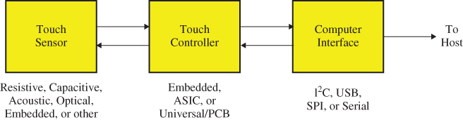
Figure 2.4 Conceptual block diagram of a touchscreen for any touch technology.
2.2.2 Classifying Touch Technologies by Size and Application
Most touch technologies have specific applications in which they work best. Or, as Bill Buxton, one of the world's most famous touch researchers, has said, “Everything is best for something and worst for something else” [5]. Table 2.1 classifies each of the 18 touch technologies covered in this chapter in two dimensions. The first dimension is the device type and size, as follows:
- Mobile devices such as tablets (2 to 17 inches).
- Stationary commercial devices such as point-of-sale terminals (10 to 30 inches).
- Stationary consumer devices such as all-in-one home desktop computers (10 to 30 inches).
- All devices larger than 30 inches (generically called “large-format” displays).
Table 2.1 In this table, the 18 touch technologies covered in this chapter are classified by device type, size, and status. Within each of four device-type and size categories, each touch technology is shown as in active current use (A), in current use but destined to disappear (L), just beginning to appear in the market (E), or not used (blank). The touch technology numbers (1 through 18) are used throughout this chapter.

The second dimension is the status of each touch technology in each of the four device type and size categories, as follows:
- A: Active, meaning widely used and accepted
- L: Legacy, meaning in current use but destined to disappear
- E: Emerging, meaning just beginning to enter the market or application
- (blank): This touch technology is not used in this size/market category
Table 2.1 can be read both vertically and horizontally. For example, reading down the Mobile column, it can be seen that p-cap, analog (single-touch) resistive, and embedded touch technologies are the primary ones used in mobile devices (A); the multi-touch forms of resistive and infrared are not fully accepted yet (E); and no other touch technologies are used in mobile devices. Similarly, reading down the Stationary Commercial column, it can be seen (for example) that there are five touch technologies in active use (A) –more than any other column. This is because commercial applications have existed for more than 30 years and the associated touch technologies have evolved to become somewhat specialized for specific applications.
Reading across the Surface Capacitive row, it can be seen (for example) that the only application for the technology is in stationary commercial devices (e.g., casino gaming machines), and that it will eventually disappear (i.e., it is a legacy technology). Similarly, reading across the In-glass Optical row, it can be seen that the technology is very new (still emerging) and currently applies only in two categories – stationary consumer devices such as all-in-one home desktop computers, and larger devices such as point-of-information displays.
Note that In-glass Optical (technology number 12) is the only one whose name is currently in flux. The underlying technology was originally named Planar Scatter ![]() by its developer (FlatFrog), but the market is beginning to use a more descriptive name.
by its developer (FlatFrog), but the market is beginning to use a more descriptive name.
2.2.3 Classifying Touch Technologies by Materials and Structure
Another method of classifying the 18 touch technologies described in this chapter is by the materials they include and by how they are structured. The most fundamental material in many touchscreens is a transparent conductor, typically indium tin oxide (ITO). Figure 2.5 splits the technologies into those that use ITO (eight on the left) and those that do not (ten on the right). Within the technologies that use ITO, the material is either in a continuous sheet or patterned. If the ITO is patterned, it is either low-resolution (millimeters) or high-resolution (microns). Within the technologies that do not use ITO, the defining structure is whether they use printed edge conductors or not. Only two do so, while the remaining eight do not.
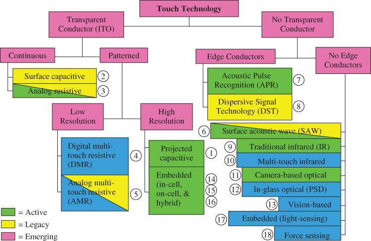
Figure 2.5 In this figure, the 18 touch technologies are classified first by their use of a transparent conductor material (typically ITO). Those technologies that use a transparent conductor are classified by whether the conductor is continuous or patterned; those that are patterned are further classified by the resolution of the patterning. Those technologies that do not use a transparent conductor are classified by their use of printed edge conductors. Note that the touch technologies are numbered to match Table 2.1. The three technologies shown in two colors (i.e., with diagonal lines) have multiple statuses in Table 2.1.
2.2.4 Classifying Touch Technologies by the Physical Quantity Being Measured
People new to the field often ask why there are so many different touch technologies. The simplest answer is that touch is an indirect measurement. If you are touching something, there is no direct method of determining exactly where you are touching, how hard you are touching, with what you are touching, or even the fact that it is uniquely you that is doing the touching. Instead, it is necessary to measure one or more of the physical quantities listed in Table 2.2 – and even then, it is still not possible to determine all four of the italicized characteristics with a single measurement. The phrase commonly used to describe this conundrum is “there is no perfect touch technology”.
Table 2.2 The 18 touch technologies depend on measuring nine different physical quantities. In order to determine the combination of where you are touching, how hard you are touching, with what you are touching, and that it is uniquely you that is doing the touching, multiple measurements with multiple touch technologies are required
| Technology number | Touch technology | Physical quantity being measured |
| 1, 14–16 | Projected Capacitive, Embedded (capacitive) | Capacitance |
| 2 | Surface Capacitive | Current |
| 3–5 | Resistive (all forms) | Voltage |
| 6 | Surface Acoustic Wave | Ultrasonic wave amplitude |
| 7,8 | Acoustic Pulse Recognition and Dispersive Signal Technology | Bending waves |
| 9–12 | Infrared, Camera-Based Optical, and In-Glass Optical (PSD) | Absence or reduction of light |
| 13 | Vision-based | Change in image composition |
| 17 | Embedded (light-sensing) | Presence of light |
| 18 | Force-sensing | Force |
2.2.5 Classifying Touch Technologies by Their Sensing Capabilities
In a 2011 article on the breadth-depth dichotomy inherent in designing touch software for platforms of varying sensing capabilities [6], Daniel Wigdor at the University of Toronto proposed the taxonomy shown in Figure 2.6. In the left half of the figure, he suggested three types of sensed objects: touches (number of touches and users), stylus (level of support), and imagery (as found only in vision-based touch technology). In the right half of the figure, he suggested four types of sensed information: contacts (from different parts of the body or different users), hover (level of support), contact data (information about the contacting object), and pressure (level of support). Each of the 18 touch technologies described in this chapter can be characterized in terms of these seven capabilities. The figure can be used to characterize a touch technology such as p-cap, as used in the iPhone and iPad, as follows:
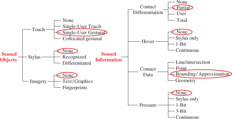
Figure 2.6 Daniel Wigdor's proposed taxonomy for classifying touch technologies based on the objects they can sense and the type of information they can deliver about those objects. The circles represent the characteristics of p-cap, as used in the iPhone, iPad, and similar mobile devices. Source: Wigdor, D., 2011. Reproduced with permission from the Society for Information Display.
- Single-user only, with gesture recognition capabilities.
- Passive stylus recognized, but not differentiated from a finger.
- No imaging capability.
- No ability to differentiate contacts from different body parts or different users.
- No hover capability.
- Approximates the size of a contact with a bounding rectangle.
- No pressure-sensing capability.
2.2.6 The Future of Touch Technologies
Even though touch technologies have been in existence for half a century and in widespread use for a quarter of a century, they are not yet all mature and fully commoditized. One reason that has already been mentioned is that “there is no perfect touch technology.” Another reason is that the touch industry is highly competitive and is strongly motivated by the creation of unique intellectual property. There is a continuous stream of startup companies developing improved forms of touch (e.g., new ways of measuring bending waves that better meet the needs of consumer applications, or entirely new ways of measuring touch-force), improvements in touch processing (e.g., reducing touch latency), developing new materials (e.g., new forms of printable transparent conductors that have the potential of cutting the cost of a p-cap touch module in half), and many other innovations. Some examples of where touch is going in the future include the following:
- Application in an ever-widening range of products from, one-inch wearable devices to 200-inch video walls.
- Full integration of touch and stylus.
- Embedded touch becoming lower cost and higher yield, competing even more aggressively with discrete touch.
- P-cap undergoing enhancements, such as the ability to use a #2 pencil as a touch object.
- Touch technologies that include more of the sensing capabilities listed in Figure 2.6.
- Seamless integration of on-screen (2D) touch with in-air (3D) gestures and other modes of interactivity.
- More use of touch on opaque objects, with the capability of making any object touch-aware.
- Lower cost, especially in touch for larger displays.
- Enhanced software-development environments that make it easier and faster to create a touch user-experience where “it just works” (i.e., touch that is robust, reliable, always performs in exactly the same way, and does not require the user to think about it).
2.3 History of Touch Technologies
Touch has a rich and varied history, which is not very surprising since there are six different basic touch technologies, each with several individual variations. Table 2.3 presents the history of touch from 1965 to the present (almost 50 years!). The table is divided into the six basic touch technologies. Within each technology, the companies or organizations that were most significant in the invention and/or commercialization of the technology are listed in chronological order, along with a brief explanation of their significance.
Table 2.3 This table presents the most complete list that has ever been published of the significant companies in the history of the six basic types of touch technology. For each significant company, an explanation of the reason for their significance and the year in which it occurred are shown
| Company | Significance | Year |
| Capacitive | ||
| Royal Radar Establishment, UK (E.A. Johnson) | First published application of transparent touchscreen (mutual-capacitance p-cap on CRT air-traffic control terminals) [1] | 1965 |
| CERN (Bent Stumpe) | Second published application of mutual-capacitance p-cap (in the control room of the CERN proton synchrotron) [7] | 1977 |
| MicroTouch Systems (acquired by 3M Touch Systems in 2001) | First commercialization of surface-capacitive [8] | Mid-1980s |
| Dynapro Thin Films (acquired by 3M Touch Systems in 2000) | First commercialization of mutual-capacitive p-cap (renamed as Near-Field Imaging by 3M) | Mid-1990s |
| Zytronic (first license from Ronald Binstead, an inventor in the UK) | First commercialization of large-format self-capacitive p-cap [9]; first commercialization of large-format mutual-capacitive p-cap [9] | 1998; 2012 |
| Visual Planet (second license from Ronald Binstead) | Second commercialization of large-format self-capacitive p-cap [9] | 2003 |
| TouchKO (acquired by Wacom in 2007) | Invention of reversing ramped-field (surface) capacitive (RRFC™) [16] | 2004 |
| Apple | First use of mutual-capacitive p-cap in a consumer electronics product (the iPhone™) [3] | 2007 |
| Resistive | ||
| Westinghouse Electric | Invention of first transparent analog-resistive touchscreen (3-wire); never commercialized [20] | 1967 |
| Sierracin/Intrex | First to commercialize digital (matrix) resistive; probably first to commercialize 4-wire analog resistive [21] | 1973; 1979 |
| Elographics (acquired by Raychem in 1986, who was acquired by Tyco Electronics in 1999, who spun off Elo Touch Solutions in 2012) | First to invent and commercialize 5-wire analog resistive [18] [19] | 1977–1982 |
| JazzMutant (renamed as Stantum in 2007) | First commercialization of digital multi-touch resistive; first commercial product with multi-touch interface [29] | 2005 |
| JTouch | First use of analog multi-touch resistive in a consumer-electronics product | 2008 |
| Acoustic | ||
| Zenith (SAW IP acquired by Elographics/Raychem in 1987, which was acquired by Tyco Electronics in 1999, which spun off Elo Touch Solutions in 2012) | Invention of surface acoustic wave (SAW, by Robert Adler, who also invented the ultrasonic TV remote-control “clicker” in 1956) [33] [34] | 1985 |
| SoundTouch Ltd. (acquired by Elo Touch Solutions in 2004) | Simultaneous invention of sampled bending-wave touch (by Tony Bick-Hardie, renamed as Acoustic Pulse Recognition™ (APR) in 2006 by Elo Touch Solutions) [40] | Early 2000s |
| Sensitive Object (acquired by Elo Touch Solutions in 2010) | Simultaneous invention of sampled bending-wave touch (originally named ReverSys™; incorporated into APR by Elo Touch Solutions) [41] | Early 2000s |
| NXT PLC (licensed to 3M Touch Systems in 2003) | First commercialization of real-time bending-wave touch (named Dispersive Signal Technology™ (DST) by 3M Touch Systems) [42] | 2006 |
| Optical | ||
| University of Illinois | First use of infrared touch (in the PLATO IV computer-assisted instruction system) [43] | 1972 |
| Sperry Rand | Invention of first form of camera-based optical touch using CCDs | 1979 |
| Hewlett-Packard | First use of infrared touch in a commercial product (in the HP-150 microcomputer) [44] | 1983 |
| Carroll Touch (acquired by AMP in 1984, which was acquired by Tyco Electronics in 1999, which spun off Elo Touch Solutions in 2012) | Broadly commercialized use of infrared touch | 1980–1999 |
| Poa Sana | First invention of waveguide infrared touch [48] | 1997–1999 |
| SMART Technologies | Simultaneously commercialized current form of camera-based optical touch using CMOS | 2003 |
| NextWindow (acquired by SMART Technologies in 2010) | Simultaneously commercialized current form of camera-based optical touch using CMOS; supplied Hewlett-Packard, who created the first consumer computer with optical touch (the TouchSmart™ all-in-one (AiO)) | 2003; 2007 |
| Perceptive Pixel (founded by Jeff Han and acquired by Microsoft in 2012) | First viral public exposure of multi-touch (in Jeff Han's TED conference videos of vision-based touch using projection) | 2006 |
| Microsoft | First commercialization of vision-based touch using projection (in Microsoft Surface v1.0) | 2007 |
| RPO (announced in 2007; assets liquidated in 2012) | Second invention of waveguide infrared touch [46] [47] | 2007–2012 |
| PQ Labs | First commercialization of multi-touch infrared [49] | 2009 |
| FlatFrog | Invention of in-glass optical touch (Planar Scatter Detection™, first shipped in 2012) [55] | 2007 |
| Baanto | First commercialization of PIN-diode optical touch [53] [54] | 2011 |
| MultiTouch | First commercialization of vision-based touch using integrated cameras (in |
2011 |
| Samsung | First commercialization of vision-based touch using in-cell light-sensing (in SUR40, used in Microsoft Surface™ 2.0, which was renamed as Microsoft PixelSense™ in 2012) [60] [77] | 2012 |
| Embedded | ||
| Planar | First to publish a technical paper on in-cell light sensing [66] | 2003 |
| Toshiba Matsushita Display | First to claim invention of in-cell light-sensing [74] | 2003 |
| Samsung | First commercial product with any form of in-cell embedded touch (in ST10 digital camera using pressed capacitive) [64] [65]; first commercial product with on-cell mutual-capacitive p-cap (on an OLED display in the S8500 Wave™ smartphone) | 2009 2010 |
| Sharp | First commercial product with in-cell light-sensing (in PC-NJ70A netbook) | 2009 |
| IDTI | Second commercial product with in-cell light-sensing (21.5-inch LCD monitor) [76] | 2010 |
| Sony (now part of Japan Display Inc.) | Invention of hybrid in-cell/on-cell mutual-capacitive p-cap (first used in Sony Xperia P™ and HTC EVO Design 4G™ smartphones) [71] | 2012 |
| Synaptics | Developed first touch controller for hybrid in-cell/on-cell capacitive (with Sony) [69] [70] | 2012 |
| Apple | First commercial product with in-cell mutual-capacitive p-cap (in the iPhone-5) [72] | 2012 |
| Other Touch Technologies | ||
| IBM | First commercial product using force-sensing touch (In TouchSelect™ overlay) | 1991 |
| MyOrigo (sold to its management in 2004; restarted as F-Origin in Finland in 2005, which went bankrupt and was restarted in the USA in 2006, which was acquired by TPK in 2009) | Only current mature supplier of force-sensing touch in 2013 (excluding several emerging startups) [81] | 2009 |
| QSI (who spun off Vissumo in 2008, which went bankrupt in 2009); QSI was acquired by Beijer Electronics in 2010 |
First successful commercial product using force-sensing touch (in touch terminals used in toll booths) [79] [80] | 2008 |
Note: References in this table are duplicates of references in the body of the chapter; there are no unique references that appear only in this table.
2.4 Capacitive Touch Technologies
2.4.1 Projected Capacitive (P-Cap) (#1)
The history of p-cap is less clear to a general audience than that of many other touch technologies, partially because the extreme significance of Apple's use of it in the first iPhone tends to obscure all previous uses of the technology. The basic concept of sensing touch by measuring a change in capacitance has been known since at least the 1960s. In fact, the first transparent touchscreen, invented in 1965 for use on air traffic system control terminals in the United Kingdom, used what today is known as mutual-capacitive p-cap [1]. The second published application of mutual-capacitance p-cap was in 1978; the application was in the control room of the CERN proton synchrotron [7].
Surface-capacitance touch technology (with an unpatterned touch-sensor) was commercialized by MicroTouch Systems in the mid-1980s [8]. During the mid-1990s, several US companies developed transparent capacitive touchscreens with patterned touch-sensors using indium tin oxide (ITO, the foundation of today's p-cap). Two of these were Dynapro Thin Films and MicroTouch Systems, both of which were later acquired by 3M (in 2000 and 2001 respectively) to form 3M Touch Systems. Dynapro Thin Films' p-cap touchscreen technology, renamed as “Near Field Imaging” (NFI), became 3M's first p-cap product in 2001. Also in 1994, an individual inventor in the UK named Ronald Peter Binstead developed a form of self-capacitance p-cap using micro-fine (25 micron) wire as the sensing electrode [9]. He licensed the technology to two UK companies: Zytronic in 1998, and Visual Planet in 2003; both are still selling it today.
P-cap remained a little-known niche technology until Apple used it in the first iPhone in 2007 [3]. Apple's engaging and immersive user-interface was an instant hit, causing most other smartphone manufacturers to begin adopting the technology. Over the next five years, p-cap set a new standard for the desirable characteristics of touch in the minds of more than one billion consumers, as follows:
- Multiple simultaneous touches (“multi-touch”, initially used only for zoom).
- Extremely light touch with flick/swipe gestures (no pressure required).
- Flush touch-surface (bezel-less).
- Excellent optical performance (especially compared with analog resistive).
- Extremely smooth and fast scrolling.
- Reliable and durable touch surface.
- Fully integrated into the device user-experience so that using it is effortless and fun.
2.4.1.1 P-cap Fundamentals
There are two basic kinds of p-cap: self-capacitance and mutual capacitance. Both are illustrated in Figure 2.7. Self-capacitance (shown in Figure 2.7A) is based on measuring the capacitance of a single electrode with respect to ground. When a finger is near the electrode, the capacitance of the human body increases the self-capacitance of the electrode with respect to ground. In contrast, mutual capacitance (shown in Figure 2.7B) is based on measuring the capacitance between a pair of electrodes. When a finger is near the pair of electrodes, the capacitance of the human body to ground “steals” some of the charge between two electrodes, thus reducing the capacitance between the electrodes [10].
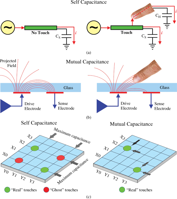
Figure 2.7 These figures illustrate the difference between self-capacitance and mutual-capacitance. A: Self-capacitance involves the capacitance of a single electrode to ground  ; a touching finger adds capacitance due to the human body capacity to ground
  . B: Mutual capacitance involves the capacitance between two electrodes; a touching finger reduces the capacitance between the electrodes by “stealing” some of the charge that is stored between the two electrodes. Adapted from 3M Touch Systems C: Self-capacitance measures the capacitance of each electrode on each axis, with the result that it allows “ghost points” because it cannot distinguish between multiple capacitance peaks on an axis (a total of 12 measurements on the
  matrix shown). Mutual capacitance measures the capacitance of every electrode intersection, which allows detecting as many touches as there are intersections (36 in the
  matrix shown).
Source: Adapted from Atmel.
The key difference between self- and mutual capacitance is how the electrodes are measured, not the number or configuration of electrodes. Regardless of how they are configured, the electrodes in a self-capacitance touchscreen are measured individually, one at a time. For example, even if the electrodes are configured in a two-layer X-Y matrix, all the X electrodes are measured and then all the Y electrodes are measured, in sequence. If a single finger is touching the screen, the result is that the nearest X electrode and the nearest Y electrode will both be detected as having maximum capacitance. However, as shown in Figure 2.7C, if the screen is touched with two or more fingers that are diagonally separated, there will be multiple maximums on each axis, and “ghost” touch points will be detected as well as “real” touch points (ghost points are false touches positionally related to real touches).
Note that this disadvantage does not eliminate the possibility of using two-finger gestures on a self-capacitive touchscreen. Rather than using the ambiguous location of the reported points, software can use the direction of movement of the points. In this situation it does not matter that four points resulted from two touches; as long as pairs of points are moving toward or away from each other (for example), a zoom gesture can be recognized. For this reason, and because self-capacitance can be lower cost than mutual capacitance, the former is often used on lower-capability mobile products.
In contrast, in a mutual-capacitive touchscreen, each electrode intersection is measured individually. Generally, this is accomplished by driving a single X electrode, measuring the capacitance of each Y (intersecting) electrode, and then repeating the process until all the X electrodes have been driven. This measurement methodology allows the controller to unambiguously identify every touch point on the touchscreen. Because of its ability to correctly process multiple touch points (moving or not), mutual capacitance is used in preference to self-capacitance in most higher-capability mobile devices today.
2.4.1.2 P-cap Controllers
In every case, the measurement of electrode capacitance is accomplished by a touch controller. Figure 2.8 illustrates the basic structure of a controller for a mutual-capacitance touchscreen. A sensor driver excites each X electrode, one at a time. An analog front end (AFE) measures the capacitance at the intersection of each Y electrode and the excited X electrode; the analog values are converted to digital by an analog-to-digital converter (ADC). A digital signal processor (DSP) runs highly sophisticated algorithms to process the array of digital capacitance data and convert it into touch locations and areas, along with a variety of related processing such as “grip suppression” (the elimination of undesired touches near the edge of the screen resulting from holding a bezel-less device) and “palm rejection” (the elimination of unintended touches resulting from the edge or base of your palm contacting the screen in the process of touching with a finger). A p-cap touch controller is an example of an application-specific integrated circuit (ASIC) [11].

Figure 2.8 The right-hand side of this figure illustrates the basic structure of a controller for a mutual-capacitance touchscreen.  represents the mutual capacitance of one electrode-pair intersection.
More innovation takes place in touch-controller design than in sensor design, because the touch controller determines how the touchscreen actually behaves, while the sensor is largely just a source of capacitance values. However, the geometry of the sensor pattern is also an ongoing contributor to performance improvement. The three best known p-cap touch-controller suppliers (Atmel, Cypress, and Synaptics, who together accounted for more than half of the p-cap touch-controller shipment revenue in 2012, excluding the special case of Apple, who designs their own p-cap touch-controller and has it manufactured by Broadcom) [12] are all US-based companies. This could be taken as a sign of the relative youth of the p-cap controller industry, since most system-level ASICs eventually become commoditized, with suppliers based in Asia. An example of recent p-cap controller innovation is the significant increase in touch-system signal-to-noise ratio (SNR) that occurred during 2012–2013. The value of this innovation is that it allows p-cap touchscreens to support a passive stylus with a 2 mm tip, rather than just a human finger.
A fine-tipped stylus adds a large amount of value to a smartphone or tablet. It allows the user to create data (drawings, notes, etc.), rather than just consume media. In Asia, it is highly desirable to be able to write Kanji characters on a smartphone, and finger-writing is impractical because the tip of your finger obscures what you are writing. A fine-tipped stylus is also excellent as a pointing device for use with software that was not designed for touch (e.g., legacy Windows applications running on a Windows-8 tablet in desktop mode).
2.4.1.3 P-cap Sensors
A p-cap sensor is comprised of a set of transparent conductive electrodes that are used by the controller to determine touch locations. In self-capacitance touchscreens, transparent conductors are patterned into spatially separated electrodes in either a single layer or two layers. When the electrodes are in a single layer, each electrode represents a different touch coordinate pair and is connected individually to a controller. When the electrodes are in two layers, they are usually arranged in a layer of rows and a layer of columns. The intersection of each row and column represents unique touch coordinate pairs. However, as noted in the previous section, in self-capacitance, each electrode is measured individually rather than measuring each intersection with other electrodes, so the multi-touch capability of this configuration is limited.
In a mutual-capacitance touchscreen, there are almost always two sets of spatially separated electrodes. The two most common electrode arrangements are:
- a rectilinear grid of rows and columns, spatially separated by an insulating layer or a film or glass substrate; and
- an interlocking diamond pattern consisting of squares on a 45° angle, connected at two corners via a small bridge.
When the interlocking diamond pattern is used on two spatially separated layers, the processing of each layer is straightforward. However, this pattern is most commonly applied in a single co-planar layer in order to achieve the thinnest possible touchscreen. In this case, the bridges require additional processing steps in order to insulate them at crossover points.
Figure 2.9 illustrates the stack-up of a typical mutual-capacitance touchscreen. To keep this and all similar drawings in this chapter as easy to understand as possible, several simplifications have been made, as follows:
- The electrode pattern shown (rows 3 and 5) is a spatially separated rectilinear grid rather than the more common interlocking diamond; row 3 shows the end-views of the Y-electrodes, while row 5 shows a side view of one X-electrode.
- The common use of optically clear adhesive (OCA) has been omitted; for example, the space between rows 2 and 3 is typically filled with OCA.
- The touchscreen is shown using a glass substrate; in many mobile devices (particularly larger ones) the substrate is often two layers of polyethylene terephthalate (PET) film, one for each set of electrodes.
- All the layers below the thin-film transistor (TFT)-array glass in the LCD (e.g., bottom polarizer, brightness enhancement films, backlight, etc.) have been omitted.
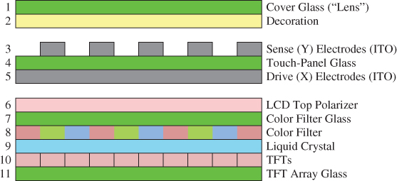
Figure 2.9 A simplified drawing of the layer stack-up for a typical mutual-capacitive touchscreen is shown on top of a simplified drawing of an LCD display. The touch sensor substrate (row 4) is assumed to be a separate piece of glass with ITO on each side.
One of the key aspects of Figure 2.9 is that it shows the touchscreen adding a fourth sheet of glass to the stackup. All LCDs use two sheets of glass, and essentially every mobile device adds a third sheet of glass (or plastic) as a protective and decorative covering over the LCD. Adding a fourth sheet of glass is generally considered to be undesirable, since it adds weight, thickness and cost to the mobile device. There are two basic methods of eliminating the fourth sheet of glass:
- The method used by the touchscreen industry, generally called “one-glass solution” (OGS), but also known by a variety of company-specific names, such as “sensor on lens”.
- The method used by the LCD industry, called “embedded touch”. These methods are in direct competition.
Figure 2.10 illustrates the one-glass solution, in which the touchscreen electrodes are moved to the underside of the decorated cover-glass (“lens”) [13]. In this solution, the touchscreen manufacturer either purchases the decorated cover-glass from an appropriate supplier, or vertically integrates and acquires the equipment and skills necessary to manufacture the cover-glass. The touchscreen manufacturer then builds the touch module (sensor plus controller), using the decorated cover-glass as a substrate and sells the entire assembly to a mobile device OEM/ODM (the touchscreen manufacturer may also buy the LCD specified by a device OEM/ODM and integrate the two together in order to provide more value to the OEM/ODM). The advantage of the one-glass solution to the end user is that the mobile device is lighter and thinner due to the elimination of the fourth piece of glass. The advantage of the one-glass solution to the touchscreen manufacturer is that they continue to derive revenue from the production of touch modules instead of forfeiting revenue to the LCD industry.
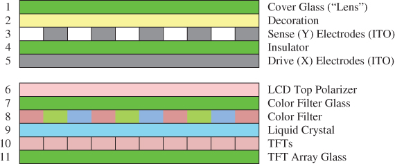
Figure 2.10 A simplified drawing of the layer stack-up for a typical “one-glass solution” (OGS) mutual-capacitive touchscreen is shown on top of the same LCD as in Figure 2.9. The touch sensor is constructed on the underside of the display cover-glass (row 1). This configuration eliminates the separate sheet of glass used for the touch sensor in Figure 2.9.
Figure 2.11 illustrates the simplest form of embedded touch (called “on-cell”), in which the fourth piece of glass is eliminated by moving the touchscreen electrodes to the top of the color-filter glass, underneath the LCD's top polarizer. Note that an on-cell configuration has exactly the same functionality as the p-cap configurations in Figure 2.9 and Figure 2.10; only the location of the electrodes is different. The advantage of the on-cell solution to the end user is exactly the same as the one-glass solution – the mobile device is lighter and thinner, due to the elimination of the fourth piece of glass. The advantage of the on-cell solution to the LCD manufacturer is that it increases their revenue due to the added value of touch functionality (but the touchscreen manufacturer loses revenue).
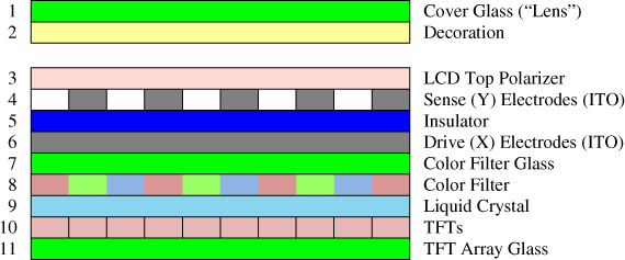
Figure 2.11 A simplified drawing of the layer stack-up for a typical on-cell embedded touchscreen is shown. In this configuration, the touch sensor is constructed on top of the color-filter glass (row 7), underneath the display's top polarizer (row 3). The functionality of this touchscreen is the same as in Figures 2.9 and 2.10; only the location of the sensor layers is different.
One other factor in embedded touch's favor is that with the touch sensor integrated into the LCD, it makes sense to consider integrating the touch controller and the display driver together into a single ASIC, or at least establishing a direct connection between the two chips to enable cooperation. Manufacturing yield can be a significant issue with on-cell embedded touch, since depositing the electrodes on the top surface of the color-filter glass substantially increases the value of that one piece of glass; if either the color-filter deposition or the touch-electrode deposition is defective, both must be discarded. Product-line management also becomes a more complex issue for the LCD manufacturer, since instead of shipping (for example) 50 million identical LCDs to a device manufacturer, the LCD manufacturer may be required to ship 10 different models, each in quantity five million with a uniquely decorated cover glass.
It is commonly believed that integrating the touch capability into the LCD should automatically make touch better and cheaper. It should be apparent from the above that on-cell embedded touch is not necessarily an automatically better solution than the one-glass solution. There are factors to be considered on both sides, and some of those factors are more business and operational-related than technical. Competition between touch-module manufacturers and LCD manufacturers will remain a major factor in the progression of all forms of embedded touch. In their Q2-2013 touch forecast, DisplaySearch estimates that all forms of embedded touch will account for only 26% of all p-cap touchscreen unit shipments by 2017 [12].
2.4.1.4 P-cap Sensors Made with Wire Instead of ITO
In all of the above discussion about p-cap touch-sensors, the transparent conductors are assumed to be made of ITO. However, as touchscreens become larger, ITO becomes an increasingly difficult material to use due to (a) relatively high sheet resistivity 50–200 ohms per square (Ω/![]() ), which slows down the touch-sensing process, and (b) lower manufacturing yields, which substantially increases the cost of the touchscreen. With rare exceptions, touchscreens made with ITO are never found above 32 inches.
), which slows down the touch-sensing process, and (b) lower manufacturing yields, which substantially increases the cost of the touchscreen. With rare exceptions, touchscreens made with ITO are never found above 32 inches.
For at least the past 10 years, the conductor material of choice for large-format (over 32-inch) p-cap touchscreens has been 10-micron copper wire. Copper wire is not transparent, but at 10 microns in diameter, it is approaching the lower limit of human visual acuity, so it is barely visible. Both self-capacitive (1–2 touch) and mutual-capacitive ![]() wire-based touchscreens are available in sizes from 40 inches to over 100 inches. In most cases, the substrate used in these large-format touchscreens is a plastic film (usually PET). The 10-micron wire electrodes are typically laid down by a manufacturing robot in two layers following a zig-zag pattern, with some form of insulation between the layers. While the touchscreen sensor may be shipped to an integrator or device maker in the form of a roll of film, the film is eventually almost always laminated to the back side of a sheet of glass for the final application. One of the fundamental reasons for this is that the top surface of all LCDs is much too soft (with a pencil hardness of only 2H or 3H) to avoid accidental damage from touches.
wire-based touchscreens are available in sizes from 40 inches to over 100 inches. In most cases, the substrate used in these large-format touchscreens is a plastic film (usually PET). The 10-micron wire electrodes are typically laid down by a manufacturing robot in two layers following a zig-zag pattern, with some form of insulation between the layers. While the touchscreen sensor may be shipped to an integrator or device maker in the form of a roll of film, the film is eventually almost always laminated to the back side of a sheet of glass for the final application. One of the fundamental reasons for this is that the top surface of all LCDs is much too soft (with a pencil hardness of only 2H or 3H) to avoid accidental damage from touches.
2.4.1.5 P-cap Touch Modules
The term “touch module” applies only to discrete touchscreens, since embedded touchscreens are an integrated part of the display. The previous sections have focused on p-cap touch-controllers and sensors; these are the primary components of a p-cap touch module. The next most important component of a touch module is the flexible printed circuit (FPC) that connects the sensor to the controller. Typically, the touch controller is mounted (along with a few passive components) on the FPC, close to the sensor in order to minimize noise pick-up. The other end of the FPC is usually inserted into a connector on the device's main board.
A p-cap touch module is usually attached to the display in only one of two ways: “air bonding” or “direct bonding”. In the first case, a double-sided adhesive gasket is applied around the top perimeter of the display, the touch module is aligned with the display, and the two pieces are pressed together. This leaves an air gap between the display and the touch sensor; the gap can range from 0.25 mm to more than 1 mm, depending on the size of the display. The advantage of air bonding is that the process is low cost with high yield; the disadvantages are that it results in additional reflecting surfaces that can significantly degrade image quality in high ambient light, and it makes the assembly slightly thicker.
In direct bonding, the entire top surface of the display is coated with an optically clear adhesive (dry or liquid). After alignment, the touch module is pressed against the display. There are multiple types of adhesive that are commonly used; the curing method depends on the type. The advantages of direct bonding are that the optical performance is always higher than air bonding, parallax error is usually reduced, and the durability of the top surface is increased (e.g., it can withstand a higher ball-drop specification). The disadvantage is that the process is high cost with low yield.
Most applications of p-cap touchscreens today are in consumer-owned devices. According to DisplaySearch, in 2013 more than 92% of these were smartphones and tablets [12]. The remaining consumer devices include notebook PCs, all-in-one desktop PCs, portable media players, portable game consoles, e-book readers, portable navigation devices, and cameras. Again according to DisplaySearch, in 2013 less than 1% of all p-cap touchscreens were in business-owned (commercial) devices [12]. The main reason for this disparity is that essentially the entire p-cap touch-module industry is focused on the 92% (smartphones and tablets). This means that the industry is generally uninterested in the smaller quantities and more demanding performance and environmental specifications that commercial applications always involve – even though businesses are willing to pay more per device.
In contrast, applications of wire-based large-format touchscreens (part of the 1%) usually involve interaction with the public. One of the best-known applications is “through store-window” retailing, where closed retailers engage potential customers outside of business hours by letting them interact with (for example) a product selection application through the store's windows. Other applications include in-store digital signage, public information kiosks, such as mall directories, and vending machines.
The advantages and disadvantages of p-cap touch technology are shown in Table 2.4 below.
Table 2.4 Advantages and disadvantages of p-cap touch technology
| P-cap advantages | P-cap disadvantages |
| Unlimited, robust multi-touch (if properly implemented) | High cost (mostly in the sensor; ITO-replacement materials will help reduce the cost) |
| Extremely light touch (zero pressure) | Touch-object must have some capacitance to ground (or be an active stylus) |
| Enables flush touch-surface (bezel-less) | Challenging to integrate (requires substantial “parameter tuning” for each new implementation) |
| Very good optical performance (especially compared with analog resistive) | Difficult to scale above 32 inches with invisible (ITO) electrodes |
| Extremely smooth and fast scrolling (if properly implemented) | No absolute pressure-sensing; only relative finger-contact area |
| Durable touch surface unaffected by scratches and many surface contaminants (protected sensor) | |
| Can be made to work with running water on the surface (but rarely done in 2013 consumer products!) | |
| Can be made to work through extremely thick glass |
|
| Can be sealed to NEMA-4 or IP65 standards |
2.4.2 Surface Capacitive (#2)
Surface capacitive was invented and commercialized by MicroTouch Systems, a company founded in 1982 and acquired by 3M in 2001 to form part of 3M Touch Systems. Because it lacked the easily damaged plastic top surface used in analog-resistive touchscreens (the dominant touch technology at that time), surface capacitive was perceived in the 1990s as the solution to more demanding touch applications.
As shown in Figure 2.12, a surface-capacitive touchscreen sensor consists of a uniform sheet of transparent conductor deposited on top of a sheet of glass. The most common transparent conductor used in surface conductive touchscreens is antimony tin oxide (ATO) deposited to produce a highly uniform sheet resistivity of 1,200–2,000 Ω/![]() . Lower-cost versions of the technology sometimes use ITO or pyrolytic tin oxide (TO) instead, with lower sheet-resistivity. The conductive coating is surrounded by, and connected to, linearization-pattern electrodes made of screen-printed silver frit that are, in turn, connected to the touchscreen flex tail (the purpose of the linearization electrodes is to correct the inherent non-linearity (bow) in the electric field associated with the properties of electrical currents flowing between corners of a rectangular conductive surface). The conductive coating and linearization electrodes are covered by a baked-on, transparent, dielectric hard coat typically made of silicon dioxide; this layer often also includes anti-glare (AG) functionality. The hard coat also almost always includes anti-stiction functionality which reduces the static friction between a finger and the surface; this makes dragging objects (e.g., cards in a video-poker game) much easier.
. Lower-cost versions of the technology sometimes use ITO or pyrolytic tin oxide (TO) instead, with lower sheet-resistivity. The conductive coating is surrounded by, and connected to, linearization-pattern electrodes made of screen-printed silver frit that are, in turn, connected to the touchscreen flex tail (the purpose of the linearization electrodes is to correct the inherent non-linearity (bow) in the electric field associated with the properties of electrical currents flowing between corners of a rectangular conductive surface). The conductive coating and linearization electrodes are covered by a baked-on, transparent, dielectric hard coat typically made of silicon dioxide; this layer often also includes anti-glare (AG) functionality. The hard coat also almost always includes anti-stiction functionality which reduces the static friction between a finger and the surface; this makes dragging objects (e.g., cards in a video-poker game) much easier.
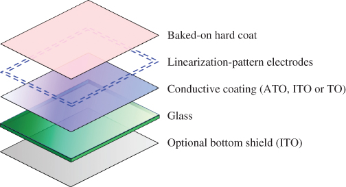
Figure 2.12 The construction of a typical surface-capacitive touch sensor is shown. The touch sensor consists of a uniform transparent-conductive coating on top of a sheet of glass. The conductive coating, surrounded by linearization-pattern electrodes, is protected by a baked-on dielectric hard coat.
Also shown in Figure 2.12 is an optional bottom shield typically made of ITO; its purpose is to shield the conductive layer from the electromagnetic interference (EMI) emitted by the display. Since the bottom shield increases the cost of the touchscreen and reduces the transmissivity (i.e., decreases image brightness), it is often seen as undesirable. Equivalent EMI reduction is often currently accomplished through firmware in the touchscreen controller.
Surface capacitive uses a uniform electrostatic field established across the conductive coating by applying an AC signal to the four corners of the conductive coating. An AC signal (typically 1–2 volts in the range of 30–100 KHz) is required because the dielectric hard-coat prevents a DC drive signal from coupling to the user's finger. All four corners are driven with exactly the same voltage, phase, and frequency. When a user's finger contacts the top coating, a small amount of electrical energy is capacitively coupled from the conductive coating to the user, causing a small amount of current to flow through each corner connection. The controller identifies a touch by comparing a known “baseline” current in the no-touch state with the change in current when a user touches the screen. The touch location is identified by measuring the amount of current supplied to each corner, and the magnitudes of these currents are proportional to the proximity of the touch location to the corners (the equivalent circuit of a surface-capacitive touchscreen is shown in Figure 2.13). The controller electronics measure these currents, converts them to DC, filters them to remove noise, amplifies them, converts them to digital via an analog-to-digital converter (ADC), calculates the touch location, adds appropriate characterization information and outputs the location coordinates to the host computer [14].
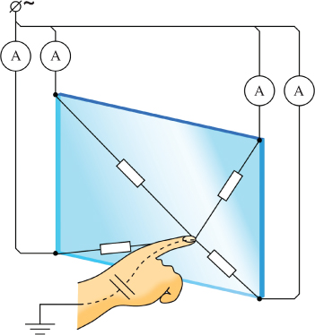
Figure 2.13 Equivalent circuit for a surface-capacitive touchscreen is shown. The circled ‘A’ symbols represent the measurement of current flowing through each corner connection.
Source: By Mercury13 (Own work) [CC-BY-SA-3.0 (http://creativecommons.org/licenses/by-sa/3.0)], via Wikimedia Commons.
The primary applications for surface-capacitive touchscreens are in regulated gaming (casinos), point-of-sales/retail terminals, point-of-information/self-check-in kiosks, and medical equipment. Regulated gaming involves a very long approval cycle for any hardware or software changes, which will slow down any possible transition from surface capacitive to p-cap. However, surface capacitive is not as durable as p-cap, because the ITO layer is on the top surface of the glass, covered only by a protective coating. Anecdotal evidence points to scratches (presumably by diamond rings) as the number one cause of failure of surface capacitive touchscreens in casino applications, which means that the greatly increased durability of p-cap is likely to be very appealing in casino applications. Another factor that will tend to drive p-cap into casino applications is the casinos' desire to attract younger customers. According to a survey reported by Harrah's Entertainment in 2006 [15], the average age of a casino patron in the USA is 46. In order to attract younger customers, casino operators believe that games must be made more interactive and exciting; p-cap's multi-touch capability can help accomplish this.
Surface-capacitive's advantages and disadvantages are shown in Table 2.5 below.
Table 2.5 Advantages and disadvantages of surface-capacitive touch technology
| Surface-capacitive advantages | Surface-capacitive disadvantages |
| Excellent drag performance with extremely smooth surface | No multi-touch |
| Much more durable than analog resistive | Finger-only (or tethered pen) |
| Resistant to contamination | Not as durable as many other glass-based touch technologies |
| Highly sensitive (very light touch) | Calibration drift and susceptibility to EMI |
| Moderate optical quality (85–90% light transmission) | |
| Cannot be used in mobile devices |
Surface capacitive is a single-touch technology. A “simulated gesture” capability similar to that in analog resistive was developed for surface capacitive by a 3M Touch Systems competitor around 2009, but it has had little effect because surface capacitive is used almost exclusively in commercial applications, where the demand for multi-touch has so far been much less than in consumer applications. However, it is likely that the demand for multi-touch in some commercial applications will change in the near future. Many users of commercial applications (e.g., casino game-players, public-access kiosk users, and medical equipment users) are likely to have smartphones and/or tablets with p-cap touchscreens, so they have a built-in expectation of multi-touch. The providers of casino games, kiosk software, and medical equipment are likely to respond to that expectation by enhancing their products with multi-touch functionality. This, in turn, will drive surface capacitive out of those applications and replace it with p-cap.
Surface capacitive technology is quite mature; 3M Touch Systems has refined it to the point where there is not much more that can be improved. 3M Touch Systems has maintained a majority share of the market ever since the acquisition of MicroTouch Systems in 2001 but, according to DisplaySearch, the total surface-capacitive market in 2013 was only about $45M, so it is not a significant factor in the overall 2013 touchscreen market of $31B [12].
Correctly sensing the future of touch, 3M Touch Systems has shifted its focus from surface capacitive to projected capacitive, as evidenced by the almost total absence of surface capacitive in 3M Touch Systems' booths at trade shows in 2013. As the market for surface capacitive shrinks, the few remaining Asian competitors are starting to exit the market, which will accelerate the rate of decline. The bottom line is that surface-capacitive touch technology is entering its end-of-life phase; within 5–7 years, the technology will be an historical curiosity.
2.4.2.1 Reversing Ramped Field Capacitive
Standard surface-capacitive technology is inappropriate for mobile use because it requires a very stable reference ground in order to establish the baseline current for the “no touch” condition. ![]() , a variation of surface capacitive employing “reversing ramped field capacitive”
, a variation of surface capacitive employing “reversing ramped field capacitive” ![]() technology, very cleverly eliminates the restriction against mobile use [16]. RRFC technology was invented by Touch Konnection Oasis (TouchKO), a small company founded in 1996 in Texas; the company was acquired by Wacom in 2007.
technology, very cleverly eliminates the restriction against mobile use [16]. RRFC technology was invented by Touch Konnection Oasis (TouchKO), a small company founded in 1996 in Texas; the company was acquired by Wacom in 2007.
In standard surface-capacitive, the conductive substrate is covered by a single, flat electrostatic field. In RRFC, four ramp-shaped fields are used instead, as shown in Figure 2.14. This is accomplished by applying an AC voltage on two adjacent corners of the conductive substrate and a DC voltage on the opposite two corners; this produces a voltage ramp across the sensor and a corresponding ramped electrostatic field. The touch controller repeats this for all four of the possible corner combinations in sequence, making four measurements of the change in current caused by a touching finger (two for X and two for Y). These measurements are shown conceptually as four perpendicular cylinders in Figure 2.14. The signals captured during the measurements are then subjected to additional digital signal processing that compensates for factors such as grounding changes, metal bezels, EMI, variations in skin dryness or finger size, thin gloves, etc. This allows the touch-event signal to be independent of all environmental capacitance effects except those due to the finger-touch.
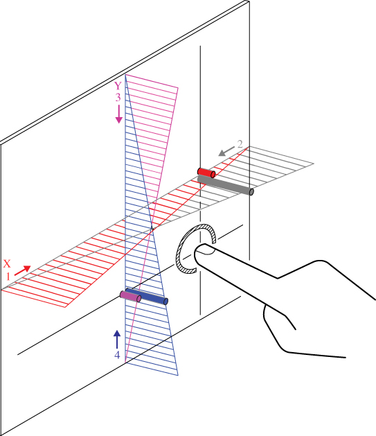
Figure 2.14 Reversing Ramped Field Capacitive (RRFC) touch technology uses four ramp-shaped fields (two voltage ramps and two electrostatic field ramps, shown as shaded triangles) instead of the single, flat electrostatic field used in legacy surface-capacitive.
Source: Reproduced with permission from Wacom.
The result is a significantly improved technology that solves most, if not all, of the problems of legacy surface capacitive. Unfortunately, there are two very big disadvantages, as follows:
- RRFC is still a single-touch technology; many surface-capacitive applications other than traditional kiosks are strongly trending towards multi-touch technologies.
- Wacom is a sole-source supplier for RRFC; unless there is an overwhelming market-driver (e.g., such as there is for Wacom's pen-digitizer used in tablets such as Samsung's Galaxy Notes), OEM/ODMs tend to avoid single-source suppliers.
2.5 Resistive Touch Technologies
2.5.1 Analog Resistive (#3)
The invention of the analog-resistive touchscreen has often been attributed to Elographics in 1975 [17]. (Elographics was founded in 1971; they were renamed as Elo Touch Systems in 1986 and then renamed again as Elo Touch Solutions in 2012). However, Elographics' original resistive technology was used in an opaque pen-digitizer, not a transparent touchscreen; it was not until 1977 that Elographics started the development of a transparent version (curved to fit the face of a CRT monitor), and that version was not shown as a commercial product until the 1982 World's Fair in Knoxville, TN [18] [19].
The first invention of a transparent analog resistive touchscreen was by Westinghouse, documented in US patent 3,522,664, filed in 1967 and granted in 1970 [20]. This touchscreen used a sheet of glass and a sheet of Mylar (transparent plastic), both coated with a uniform transparent conductor and separated by a spacer. The structure was a three-wire touchscreen (now obsolete), where the three wires were:
- two adjacent sides of the glass substrate, connected through sets of diodes;
- the other two adjacent sides of the glass substrate, also connected through sets of diodes; and
- the top Mylar sheet (see the patent for more technical details).
This invention was never commercialized; it is more likely that Sierracin/Intrex's four-wire analog-resistive touchscreen, first sold in 1979 under the brand name “TransTech”, may have actually been the first commercially available analog-resistive touchscreen. [21]
An analog resistive touchscreen is simply a mechanical switch mechanism used to locate a touch. The construction of a typical analog-resistive touchscreen is shown in Figure 2.15. A glass substrate and a flexible film (usually PET) are both coated on one side with the transparent conductor ITO. With the two coated sides facing each other, the two conductive surfaces are separated by very small ![]() , transparent, insulating spacer-dots. A voltage is applied across one or both of the sheets (depending on the type of resistive touchscreen). When a finger presses on the flexible film, the two conductive surfaces make electrical contact. The resistance of the ITO creates a voltage divider at the contact point, and the ratio of the voltages is used to calculate the touch position.
, transparent, insulating spacer-dots. A voltage is applied across one or both of the sheets (depending on the type of resistive touchscreen). When a finger presses on the flexible film, the two conductive surfaces make electrical contact. The resistance of the ITO creates a voltage divider at the contact point, and the ratio of the voltages is used to calculate the touch position.
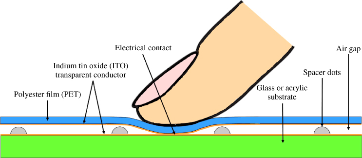
Figure 2.15 An analog-resistive touchscreen is a mechanical switch mechanism used to locate a touch. Two conductive layers are separated by tiny insulating spacer dots; when the two layers are pressed together, an electrical contact is made. The touch location is calculated from the ratio of voltages on the conductive layers. Adapted from Elo Touch Solutions.
2.5.1.1 Analog-Resistive Variations
Resistive touch technology has three key variations:
- the number of “wires”;
- the layer construction; and
- the options.
The number of wires refers to the number of connections to the sensor; the three common types are 4-wire, 5-wire, and 8-wire.
In a 4-wire touchscreen (Figure 2.16), connections are made to bus bars on the left and right (X) edges of one conductive sheet, and bus bars on the top and bottom (Y) edges of the other. To determine the X position of the touch, the controller applies a voltage across the X connections and measures the voltage at one of the Y connections. The controller then reverses the process, applying voltage across the Y connections and measuring the voltage at one of the X connections to determine the Y location [22].
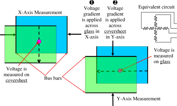
Figure 2.16 In a four-wire touchscreen, a voltage gradient is applied between the two X-axis bus bars on the glass and the resulting voltage is measured on the coversheet. The voltage gradient is then applied between the two Y-axis bus bars on the coversheet and the resulting voltage is measured on the glass.
In a 5-wire touchscreen (Figure 2.17), the X and Y voltages are applied to the four corners of the lower conductive sheet and the upper sheet is used only as a contact point (wiper). To determine the X position, the controller applies a voltage to the two right-hand X-axis corners and grounds the two left-hand X-axis corners. The coversheet (the fifth wire) is used as a voltage probe to measure the X position. The controller then reverses the process, applying a voltage to the top two Y-axis contacts and grounding the bottom two Y-axis connections. Again, the coversheet is used as a voltage probe to measure the Y position. A 5-wire touchscreen is always ready for a touch; when waiting for a touch, the four corners are driven with the same voltage, and the coversheet is grounded through a high resistance. When there is no touch on the screen, the voltage on the coversheet is zero. When the screen is touched, the controller detects the increased current flow to the coversheet and starts the measurement process, as previously described [23].
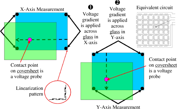
Figure 2.17 In a five-wire touchscreen, a voltage gradient is applied along the X-axis of the glass, and the coversheet (wire #5) is used as a voltage probe. Then the voltage is applied along the Y-axis of the glass, and again the coversheet is used as a voltage probe.
The key difference between 4-wire and 5-wire touchscreens is service lifetime; 4-wire is typically rated for 1M touches with a finger (or 100,000 characters with a stylus), while 5-wire is typically rated for 30 million touches with a finger. This difference is due to the way the upper conductive sheet is used; using it as only a contact point rather than a resistive voltage divider allows the condition of the conductive coating to deteriorate much further before ceasing to function.
An 8-wire touchscreen is a 4-wire touchscreen with an extra wire connected to each bus bar to allow measuring the voltage directly at the sensor. The key advantage of this technique, generally called “four-terminal sensing”, is that the separation of voltage and current eliminates the impedance contribution of the four wires carrying current from the controller to the sensor. This reduces drift in the touchscreen calibration [24].
In the past, there were also “6-wire” and “7-wire” resistive touchscreens; in general, these were created by touchscreen manufacturers who were trying to design around Elo Touch Solutions' patents on the 5-wire design. The six-wire variation added an extra ground layer on the back of the glass substrate; however, this had no real effect on performance. The seven-wire variation added two extra sense wires (like the 8-wire design) to decrease drift due to environmental changes, but it did not work very well. These unusual products performed essentially the same as 5-wire touchscreens.
Resistive touchscreens utilize seven different layer constructions, as follows:
- Film/film
- Film/glass
- Film/plastic
- Film/film/plastic
- Film/film/glass
- Glass/film/glass
- Glass/glass
The first term in the construction is the top layer (i.e., five of the constructions use PET film as the top layer); the last term in the construction is the substrate. The first two of the constructions account for 80% of the market in terms of units, with the majority of the suppliers of those constructions located in Taiwan and China [12]. The first construction is used mostly in mobile devices (especially mobile phones), while the second construction is used in both mobile devices and commercial applications. The third construction is used mainly in products where glass breakage cannot be allowed (e.g., children's toys). The fourth construction is a film/film touchscreen attached to a rigid plastic substrate for improved durability; the fifth construction is the same as the fourth, except with a plain-glass substrate for rigidity (often used with digital resistive); the sixth construction is known as “armored”, since it eliminates the durability issues of the PET top layer; the seventh construction is used mainly in automotive applications, due to its environmental robustness.
Resistive touchscreens are available with a large number of options, many more than for any other touch technology. Common options include the following (see Section 2.13 for more details):
- Hard coating – for durability.
- Anti-reflection coating – to reduce diffuse reflections.
- Anti-glare coating – to change specular reflections into diffuse reflections.
- Anti-fingerprint coating – to prevent fingerprint oils from adhering to the top surface.
- Anti-pollution (or “anti-corruption”) coating – to prevent substances such as permanent-marker ink from adhering.
- Anti-microbial coating – to reduce bacterial adhesion on medical devices.
- Ruggedized substrate – for durability.
- Surface armoring – laminating micro-glass on top of film/glass construction for durability.
- High transmissivity/low reflectivity – to improve visibility in outdoor use.
2.5.1.2 Analog-Resistive Characteristics
Analog resistive is a single-touch technology – i.e., it does not support real multi-touch. As noted in the p-cap (#1) section of this chapter, consumer expectation set by more than one billion smartphones and tablets is that touchscreens must support multi-touch. In 2008, a resistive-controller enhancement, sometimes called “simulated gestures”, was developed as a marketing workaround for the lack of multi-touch. Today, many standard resistive controllers include a simulated gesture capability [25].
There are several methods of implementing simulated gestures; one is to measure the current consumed by the sensor during operation. With a single touch, the current is normally constant and thus not monitored but, with two contact points, the two conductive sheets become resistors in parallel, which increases the current consumption. This allows analog resistive to support a few simple two-finger gestures, such as zoom and rotate, but it cannot pass standard multi-touch tests such as the Microsoft Windows Touch Logo.
Simulated gestures are important in marketing touchscreens because they allow low-end analog-resistive touchscreens to appear to be similar to p-cap touchscreens in at least one respect. In reality, the user experience with resistive simulated gestures is very different, not only because of the limited gesture capability, but also because most resistive touchscreens require significantly more touch force than p-cap, which makes it difficult to consistently press hard enough while moving two fingers at the same time.
The advantages and disadvantages of analog-resistive touch technology are shown in Table 2.6 below.
Table 2.6 Advantages and disadvantages of analog-resistive touch technology
| Analog-resistive advantages | Analog-resistive disadvantages |
| Works with finger, stylus, or any non-sharp object (“touch with anything”) | No multi-touch (only “simulated gestures”) |
| Lowest-cost touch technology: $1 or less per diagonal inch of screen dimension | Poor optical quality (up to 20% of the display's emitted light can be lost to layer reflections |
| Widely available from around 100 suppliers (it is a commodity) | Poor durability (easily damaged PET top surface) |
| Can be sealed to IP65 or NEMA-4 environmental standards | Relatively high touch-force |
| Resistant to screen contaminants | |
| Low power-consumption |
The four disadvantages shown in Table 2.6 above are all in direct conflict with the new de facto standard established by p-cap. These disadvantages are causing analog resistive to rapidly lose market share to p-cap in consumer-electronics applications; according to DisplaySearch, analog-resistive had only a 16% share of consumer unit-shipments in 2012, and 73% of that was in mobile phones [12].
The situation is quite different in commercial applications where, according to DisplaySearch, analog resistive had an 88% share of unit shipments in 2012 [12]. The major commercial applications for resistive include automotive, factory equipment, retail/point-of-sales (POS), kiosks for point-of-information (POI) and self-check-in, and office equipment such as copiers and printers. The reasons for the continuing strength of resistive technology in commercial applications are as follows:
- Resistive has been the standard for more than 30 years, so many applications have adapted to its disadvantages.
- There is much less demand for multi-touch in commercial applications, although it is starting to grow in some segments.
- Commercial applications are mostly point-and-click, with almost no use of swipe gestures, so the touch force is less critical.
- To meet the rapidly increasing demand for flush-bezel in commercial applications, most resistive suppliers have implemented a “flush appearance” version of 5-wire [26].
- There is significant demand for stylus use, and resistive works very well with any type of passive stylus.
- There has not been anything in the commercial touch world remotely like the “iPhone Big Bang” that changed everything in the consumer touch world.
Resistive touch-technology has nowhere to go but down in both consumer and commercial applications. Its primary advantages in consumer applications are its low cost and its stylus capability. However, p-cap will incorporate both of these advantages within five years, which will drive resistive's market share of consumer applications well down into single digits.
In commercial applications, resistive will lose share mainly to p-cap. The rate at which that will happen depends on:
- how quickly the cost of p-cap falls;
- how quickly more p-cap suppliers sign up to meet the more specialized needs of commercial applications;
- how quickly demand increases in each application for p-cap's key capabilities (multi-touch, high optical-performance, flush bezel, and very light touch). For example, the demand for flush bezel is likely to increase much faster in customer-facing applications, such as healthcare and point-of-information, than in point-of-sale or factory-equipment applications. Similarly, the demand for multi-touch is likely to increase much faster in casual and casino gaming (as entertainment establishments try to capture younger customers) than in point-of-sale, where it is difficult to imagine any need for multi-touch (for example) on a fast-food restaurant order-terminal.
DisplaySearch expects resistive's share of unit shipments in commercial applications to drop only moderately, from 88% in 2012 to 72% in 2017 [12].
2.5.2 Digital Multi-touch Resistive (DMR) (#4)
A form of resistive touchscreen called “matrix resistive”, in which the sheets of transparent conductor (ITO) are segmented into grids of rows and columns, was actually the first resistive touchscreen technology to be developed. Sierracin/Intrex first started selling ITO-coated PET film in 1973; according to an employee who worked there at the time, Sierracin/Intrex created a matrix-resistive tick-tack-toe game as a trade-show demo of their film [27]. This quickly led to customers developing products that incorporated matrix-resistive touchscreens. Of course, the row-and-column matrix technique was not unique at the time; it had been used much earlier with opaque (metal) conductors in membrane-switch panels.
In a digital-resistive touchscreen, the ITO coatings on the two layers (substrate and cover-sheet) are patterned into horizontal and vertical strips positioned at right angles to each other, as shown in Figure 2.18. When the touchscreen is pressed, one or more intersections of the ITO coatings make electrical contact, and each intersection forms an independent switch. The pitch (spacing) of the strips depends on the desired switch-matrix layout; there is no requirement for symmetry, so a matrix can be any number by any number (e.g., 4 rows by 12 columns). Most digital-resistive touchscreens are custom-designed and do not require controllers [28].
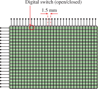
Figure 2.18 A digital-resistive touchscreen is made up of two layers (substrate and cover-sheet) coated with a transparent conductor (ITO) that is patterned into horizontal and vertical strips positioned at right angles to each other. When the touchscreen is pressed, one or more intersections of the ITO coatings make electrical contact, completing a circuit. This specific example is a representation of the touch sensor in Stantum's iVSM (see the text below).
In the 1970s, digital resistive touchscreens were used mostly in commercial applications such as factory automation, copying machines, fax machines, calculators, and cash-dispensers. Once 4-wire and 5-wire analog-resistive touchscreens started to spread in the 1980s, digital-resistive touchscreens became less popular, due to their lower resolution and inability to handle writing or drawing.
Digital resistive was a single-touch technology until JazzMutant, a French supplier of music controllers founded in 2002, launched the ![]() in 2005. While multi-touch had been used in research projects since 1982 [5], the Lemur music controller was actually the first commercial product to use a multi-touch interface [29]. When JazzMutant decided to market their multi-touch technology separately in 2007 (the same year during which the first iPhone was announced), they renamed the company as Stantum.
in 2005. While multi-touch had been used in research projects since 1982 [5], the Lemur music controller was actually the first commercial product to use a multi-touch interface [29]. When JazzMutant decided to market their multi-touch technology separately in 2007 (the same year during which the first iPhone was announced), they renamed the company as Stantum.
Stantum's technology is digital multi-touch resistive (DMR), branded as “Interpolated Voltage-Sensing Matrix” ![]() . With the exception of the addition of a sophisticated multi-touch controller, the technology uses the same basic transparent switch-matrix concept that was introduced to the market more than 30 years earlier. The key differences are as follows:
. With the exception of the addition of a sophisticated multi-touch controller, the technology uses the same basic transparent switch-matrix concept that was introduced to the market more than 30 years earlier. The key differences are as follows:
- The pitch of the ITO vertical and horizontal strips is only 1.5 mm, much narrower than had been used previously. While this allows the controller to do interpolation between intersections to achieve much higher resolution, it also greatly increases the number of connections to the controller (e.g., 400 connections for a ten-inch screen).
- The touch-activation force is relatively light at 8–15 grams.
- The controller, which supports up to ten simultaneous touches, is optimized for both finger-touch and stylus-touch. This means that it incorporates “palm rejection” (the ability to ignore any touches other than the tip of the stylus), which is critically important for effective stylus use.
Because they were a small startup in France, Stantum decided to use a licensing business model rather than become a touchscreen hardware supplier. Stantum initially licensed their controller to two ASIC manufacturers (ST Microelectronics and Sitronix) and partnered with Gunze USA, a touchscreen manufacturer focused on commercial applications. Between 2009 and 2011, Stantum had some limited success in commercial and military applications, where the combination of finger and stylus is in more demand. In 2012, Stantum partnered with Nissha Printing in developing a version of iVSM called “Fine Touch Z”, which includes a layer of Peratech's transparent pressure-sensing material between the two substrates, greatly increasing the pressure-sensing capability of the touchscreen [30]. While keeping a lower profile than in previous years, Stantum continues to work with their partners on designing products for commercial applications such as tablets for K-12 education. While Stantum is not the only supplier of digital multi-touch resistive technology, they are without doubt the most well-known.
The advantages and disadvantages of digital multi-touch resistive technology are listed in Table 2.7.
Table 2.7 Advantages and disadvantages of digital multi-touch resistive touch technology
| Digital multi-touch resistive advantages | Digital multi-touch resistive disadvantages |
| True multi-touch | Poor optical quality (up to 20% of the display's emitted light can be lost to layer reflections |
| Works with finger, stylus, or any non-sharp object (“touch with anything”) | Poor durability (easily damaged PET top surface) |
| Lower cost than p-cap | Touch-force low but still higher than p-cap |
| Simple and familiar resistive technology | High number of sensor connections |
| Can be sealed to IP65 or NEMA-4 environmental standards | Limited number of suppliers |
| Resistant to screen contaminants | Custom sensor design usually required |
| Low power-consumption |
2.5.3 Analog Multi-touch Resistive (AMR) (#5)
When the iPhone in 2007 ignited the seemingly insatiable desire for multi-touch everywhere, the analog-resistive touchscreen industry created a hybrid of digital and analog resistive touch-technology called “analog multi-touch resistive” as a lower-cost alternative to p-cap. JTouch in Taiwan, in 2008, was the first touchscreen supplier to commercialize the technology. Generically, this technology is usually known by the acronym AMR; however, some touchscreen suppliers have branded their own version of the technology. For example, Touch International calls it “multi-touch analog-resistive sensor” (MARS). Some suppliers simply advertise “matrix-resistive touchscreens” which requires checking the datasheet to determine whether it is analog or digital. One method of making the determination is to look at the connections coming from the edges of the sensor. If there are many connections on all four edges, then it is analog. If there are many connections on only two edges, then it is digital.
In this technology, shown in Figure 2.19, each conductive surface is patterned into strips so that each overlapping intersection of strips forms a square; each square acts as a miniature four-wire touchscreen. That is, the location of a touch within any square is determined by the same analog voltage-divider method used in single-touch resistive. The technology can handle up to as many separate touches as there are squares. However, if two touches occur in a single square, the two touches are averaged and a single touch is reported – exactly the same as in a four-wire touchscreen.
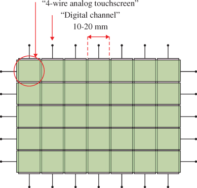
Figure 2.19 In an analog multi-touch resistive (AMR) touchscreen, the normally uniform conductive layers are patterned into strips so that each intersection of strips forms a square, typically 10–20 mm on each side. Each square acts like an independent four-wire analog touch screen.
The physical construction of an AMR touchscreen is very similar to that a four-wire analog resistive touchscreen, with the exception of the patterning of the ITO layers. AMR touchscreens are often available only in film-glass construction, although sometimes glass-film-glass is offered for higher durability. AMR touchscreen controllers are available from standard sources such as Texas Instruments [31]. Some touchscreen manufacturers, such as AMT (Apex Material Technology), make their own AMR controllers [32].
AMR was initially targeted as a low-cost multi-touch solution for all-in-one (AiO) consumer desktop computers running Windows 7. In order to minimize the number of sensor connections in the typical 22-inch AiO touchscreen (i.e., to reduce cost), the squares were typically sized at 10–20 mm wide. Unfortunately, this meant that if the user held two fingers closely together and dragged them across the screen, the touchscreen output randomly switched between one or two touches, depending on the location of the touches. In many cases, the consumer user interpreted this behavior as an indication that the touchscreen was defective. In addition to this fundamentally flawed user-experience, AMR in the consumer electronics market also had the following problems:
- It was not significantly lower cost than p-cap.
- It was quite difficult to make properly, especially in larger sizes.
- It had all the same fundamental limitations of resistive (relatively high touch force, low optical performance, and low durability).
After only a few months on the market, one major OEM withdrew their AMR-based AiO products; essentially all other AMR-based AiO products failed to get any meaningful level of consumer acceptance within a year or two. The resistive touchscreen industry learned from this experience; in 2013 the only AMR touchscreens on the market were:
- smaller;
- made with squares small enough so that it was impossible to get two fingers on one square; and
- targeted at specialized commercial and military applications.
In summary, although the technology was developed to compete with the multi-touch capability of p-cap at a lower cost in consumer products, it failed badly and has now become an insignificant niche technology.
The advantages and disadvantages of analog multi-touch resistive technology are listed in Table 2.8.
Table 2.8 Advantages and disadvantages of analog multi-touch resistive touch technology
| Analog multi-touch resistive advantages | Analog multi-touch resistive disadvantages |
| Multi-touch, but without two touches on the same square | Poor optical quality (up to 20% of the display's emitted light can be lost to layer reflections |
| Works with finger, stylus, or any non-sharp object (“touch with anything”) | Poor durability (easily damaged PET top surface) |
| Simple and familiar resistive technology | Touch-force low but still higher than p-cap |
| Can be sealed to IP65 or NEMA-4 environmental standards | High number of sensor connections (with a pitch tight enough to handle two fingers held together) |
| Resistant to screen contaminants | Limited number of suppliers |
| Low power consumption |
2.6 Acoustic Touch Technologies
2.6.1 Surface Acoustic Wave (SAW) (#6)
Surface acoustic wave (SAW) in its current form was invented in 1985 by Dr. Robert Adler, a well-known inventor at Zenith [33]. (Dr. Adler is best known for being the co-inventor of the ultrasonic TV remote control, first sold in 1956 [34].) Zenith sold SAW touchscreen technology in 1987 to Elo Touch Solutions which, at the time, was owned by Raychem and known as Elographics. After the sale, Robert Adler continued consulting for Elo, actively contributing to the commercialization of SAW technology into the 1990s.
As shown in Figure 2.20, a SAW sensor is relatively simple, consisting of a piece of ordinary soda-lime glass, four piezo transducers, and four wave-directing partial-reflectors made of low-temperature glass frit that is screen-printed on the surface and then fired. The piezo transducers are configured in pairs, one for the X-axis and one for the Y-axis. The X and Y transmitting transducers send bursts of ultrasonic Raleigh waves across the surface of the glass, aimed down the X and Y transmitting reflectors. Frequencies in the range of 4–10 MHz are known to work, but for historical reasons, most SAW touchscreens today operate at 5.53 MHz. The transmitting reflectors consist of an array of ridges at a 45-degree angle; as the Rayleigh waves hit the ridges, some of them are reflected across the screen. The spacing between adjacent ridges is an integral multiple of one wavelength of the propagating wave on the glass. This prevents destructive interference of the wave train as it travels down the reflector array and is partially reflected at each ridge. A matching set of receiving reflectors on the opposite edges of the screen direct the waves towards the X and Y receiving transducers.
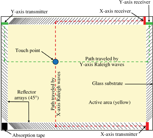
Figure 2.20 A surface acoustic wave (SAW) touch sensor consists of a glass substrate, two transmitting transducers (one per axis), two receiving transducers, and four 45-degree reflector patterns. Rayleigh waves travel from a transmitting transducer down a reflector, across the screen, and up the opposite reflector to a receiving transducer. Adapted from Elo Touch Solutions.
The transit time of any given Rayleigh wave from transmitting transducer to receiving transducer depends on the length of the path; waves reflected by the beginning of the reflector take less time than waves reflected by the end of the reflector. The use of a “time of flight” method such as this is possible when the medium behaves in a non-dispersive manner, i.e., when the velocity of the waves does not vary significantly over the frequency range of interest. In this way, the physical location of the touch on the screen is mapped into the time domain. When a human finger or other soft (sound-absorbing) object touches the glass, it absorbs a portion of specific X and Y Rayleigh waves.
As shown in Figure 2.21, the touch location is determined by measuring where the reduction in wave amplitude occurs in the time domain for the X and Y waves. By measuring the amount of amplitude reduction, an indication of the touch pressure in the Z-axis can be obtained – although this is rarely done in practice.
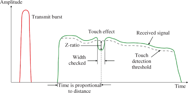
Figure 2.21 In a SAW touchscreen, a transmit burst of Rayleigh waves in the X or Y axis produces an amplitude response curve in the time domain; the location of a touch on an axis is determined by the time-domain location of an amplitude dip.
Source: Adapted from Elo Touch Solutions.
SAW controllers are adaptive. They continually monitor the received waveform in the “no-touch” condition in order to ignore most forms of contamination on the touch surface, adjust for changes in environmental conditions, and change the noise threshold when necessary.
SAW touchscreens are available in sizes from 6 to 52 inches. However, because of the relatively high attenuation (absorption) of Raleigh waves in soda-lime glass, screens larger than about 24 inches typically use borosilicate or barium glass, due to its lower attenuation (this type of glass adds up to 30dB to the signal-to-noise ratio of a 42-inch SAW touchscreen system [35]). However, as the touchscreen size approaches 42 inches, optical touch-technologies become more cost-effective so, even though it is technically possible to build a 52-inch SAW touchscreen, it is becoming increasingly rare in actual applications.
SAW was originally a single-touch technology, but the two largest suppliers, Elo Touch Solutions and General Touch (which together account for the majority of the market) both developed two-touch versions in 2009 and 2010 respectively. Elo's approach is to add a second set of reflectors at angles other than 45° (e.g., 15° or 75°) in order to provide an additional source of touch location data [36]. The primary drawback of two-touch SAW is that SAW requires a significant amount of force to register a touch – between 20 and 80 grams, depending on the implementation. Even for a single-touch application, this is much more force than p-cap requires (which is essentially zero). Maintaining sufficient pressure with two fingers while performing a gesture such as zoom or rotate, or having to press hard to perform a swipe gesture, are not very good user experiences. Some models of all-in-one Windows 7 consumer desktop computers from Lenovo and Samsung were marketed with two-touch SAW, but there has not been any significant consumer-market penetration beyond that. Windows 8 has ended any consideration of SAW in the consumer market, since the Windows 8 touch specifications require a minimum of five touches [37].
Another problem with standard SAW is that it requires a bezel to cover the reflectors around the border of the glass. Both Elo Touch Solutions and General Touch have developed a bezel-less (alternatively called “zero-bezel”, “flush”, or “edge-to-edge”) two-touch version. Elo Touch Solutions' approach is to move the transducers and reflectors to the underside of the glass and around the edge of the glass, so that the waves flow smoothly from the front surface to the back surface of the glass. Because there is little available space on the underside of the glass due to the frame of the LCD, instead of using two sets of reflectors, Elo Touch Solutions uses a single set and multiplexes them [38]. The shaped edge and location of the transducers and reflectors make this configuration more difficult to integrate than p-cap in a bezel-less device.
As previously noted, resistive touch technology currently has a majority share of the revenue in the commercial-application touch market, but SAW and surface capacitive compete for most of the remainder. SAW's primary applications are public-access kiosks (point-of-information), point-of-sales (POS), ATMs, and gaming machines. SAW has a broader range of applications than surface capacitive because it has lower cost, better optical performance, higher durability, easier integration, and more suppliers. These advantages, coupled with its two-touch capability, means that SAW is likely to continue to be used in commercial applications. Table 2.9 lists the advantages and disadvantages of SAW touchscreens.
Table 2.9 Advantages and disadvantages of surface acoustic wave (SAW) touch technology
| SAW advantages | SAW disadvantages |
| High optical performance due to plain-glass substrate | No multi-touch ( |
| Finger, gloved hand, and soft-stylus activation | Very sensitive to surface contamination, especially by water |
| Very durable; can be vandal-proofed with tempered or chemically strengthened (CS) glass | Relatively high activation force (20–80 g typical) |
| Relatively easy to integrate; available in waterproof and/or dustproof versions | Requires a soft (sound-absorbing) touch object |
2.6.2 Acoustic Pulse Recognition (APR) (#7)
Both acoustic pulse recognition (APR) and dispersive signal technology (DST, covered in the next section) make use of bending waves. Bending waves are a form of mechanical energy created when an object impacts the surface of a rigid substrate. Bending waves differ from surface waves in that they travel through the full thickness of the substrate, rather than just on the surface of the material; one advantage that results from this difference is superior scratch resistance.
When an object such as a finger or stylus touches the substrate, bending waves are induced that radiate away from the touch location. As the waves travel outward, they spread out over time due to the phenomena of dispersion, where the velocity of a bending wave propagating through solid material is dependent upon the wave's frequency. An impulse caused by a touch contact generates a number of bending waves within the substrate, all at different frequencies. Because of dispersion, these bending waves propagate out to the edges of the glass at different speeds, rather than in a unified wave front. The result is that sensors at the edges or corners of the substrate receive a wave formation that does not resemble the original impulse at all; the wave formation is further modified by reflections from the internal surfaces of the substrate. The net result is a chaotic mass of waves, all interfering with one another throughout the substrate. The key difference between APR and DST touch technology is how that chaotic mass of waves is processed.
In acoustic pulse recognition (APR) touchscreens, the glass substrate is “characterized” in advance by tapping the substrate in thousands of locations, using a robot. The bending-wave “signature” of each location is sampled and stored in a lookup table in non-volatile RAM that is associated with the particular substrate. In operation, bending waves produced by a touch are sensed by four piezoelectric transducers located asymmetrically on the perimeter of the substrate (see Figure 2.22). The asymmetry helps ensure that the signatures are as complex as possible; a high level of complexity helps differentiate the signatures. A controller processes the output of the four transducers to produce the signature of the current touch and then compares it with the stored samples in the lookup table; interpolation between samples is used to calculate the correct touch location [39].
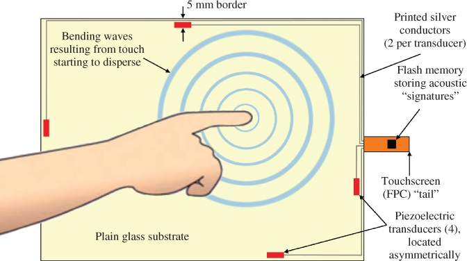
Figure 2.22 An Acoustic Pulse Recognition (APR) touch sensor consists of a piece of glass with four piezoelectric transducers on the back surface of the glass. When a finger or any object contacts the glass, bending waves are produced in the glass substrate and sampled by the transducers; a controller determines the touch location. Adapted from Elo Touch Solutions.
The concept of APR was developed in the early 2000s by Tony Hardie-Bick, an individual inventor in the UK with his own company, SoundTouch Ltd. Elo Touch Solutions acquired the assets of SoundTouch around 2004. After some development for commercialization, the technology was announced in 2006. It was designed to be a more-durable, low-cost replacement for analog resistive, before Apple made multi-touch capability a market requirement in 2007.
A touch technology based on the same fundamental idea of sensing bending waves was developed simultaneously and independently by Sensitive Object in France (it was branded “ReverSys”) [40]. Sensitive Object's intellectual property (IP) and Elo Touch Solutions' IP did not infringe each other, but they were closely interleaved, so the two companies executed a cross-license agreement in 2007, shortly after the launch of both products. The two companies continued to develop separately after the agreement was signed, because the purpose of the agreement was to avoid a lawsuit over the existing IP, not to share IP going forward. One of Sensitive Object's key innovations was a method of quickly characterizing a substrate in just a few steps, versus Elo Touch Solutions' method of tapping the substrate thousands of times with a robot arm. Elo Touch Solutions purchased Sensitive Object in January of 2010 for $62M [41]. The combination of the two companies' IP produced a very strong portfolio.
However, even with its strong portfolio, APR has a number of fundamental limitations due to its reliance on bending waves. The most important of these limitations is that APR does not have a “hold” function (equivalent to keeping a mouse button depressed). When the touching object stops moving, bending waves are no longer produced. This means that the commonly used sequence of drag-pause-drag on the Windows desktop does not work, since the APR driver must issue an automatic mouse-up at the beginning of the pause. This essentially limits the technology to commercial use (i.e., non-Windows user interfaces) rather than consumer use.
Another key limitation of APR is that it requires a “tap” to produce enough bending waves to be detected. If a shy or uncertain user “sneaks up” on an APR touchscreen and presses it without a distinct tap (even if the user presses very hard), the touch will not register. After the lack of “touch-and-hold” and the need for a distinct tap, the next most important limitation is that APR is fundamentally a single-touch technology. In a world increasingly dominated by multi-touch technologies, single-touch is becoming less and less relevant.
There are three additional limitations due to APR's reliance on bending waves. The first limitation is that APR touch technology is not deterministic. Touching the same exact location many times produces a “cloud” of points surrounding the target coordinates. This means that drawing with a stylus will not produce exactly the same result every time. This is quite different from analog resistive, where touching the same exact location always produces the same coordinates.
The second limitation is that APR's bending-wave detection algorithms cannot be optimized for both:
- the intermittent bending waves that result from a series of rapid taps, such as occur in a point-of-sales (POS) application; and
- the continuous bending waves that result from drags, such as occur when writing a signature in the same POS application.
Optimizing for “general-purpose applications” results in a compromise, where the performance of rapid taps and drags are both sub-optimum.
The third and final limitation is that the mounting (clamping) of an APR touchscreen is critical to good performance. This can easily be understood by considering the difference in sound vibrations produced by tapping a free-hanging sheet of glass versus a sheet that is clamped tightly on all four sides. This means that product manufacturers and system integrators worldwide must be trained on how to properly integrate an APR touchscreen. For this reason, APR is not currently available as a component, only integrated into touch systems (finished products) produced by Elo Touch Solutions.
Given the dominance of p-cap and the substantial number of limitations described above, APR as it is today is unlikely to become a mainstream touch technology. However, Elo Touch Solutions is gaining some limited market share with APR in POS applications where none of the above limitations matter. Beyond touchscreens on displays, Elo Touch Solutions may be able to exploit various other non-traditional application niches through the incorporation of ReverSys' ability to make any rigid object into a touch-sensing surface. For example, the back case of a smartphone could be made touch-sensitive in this way.
Since APR and DST are so similar, the advantages and disadvantages of both touch technologies are combined in Table 2.10.
Table 2.10 Advantages and disadvantages of Elo Touch Solutions' Acoustic Pulse Recognition (APR) and 3M Touch Systems' Dispersive Signal Technology (DST), both of which are based on sensing bending waves
| APR & DST advantages | APR & DST disadvantages |
| Works with finger, stylus, or any touch object | No “touch-and-hold” |
| High optical quality due to plain-glass substrate | No multi-touch |
| Very simple sensor (glass |
Requires enough touch-object velocity (a tap) to generate bending waves |
| Resistant to surface contamination; works with scratches and extraneous objects on the surface | Mounting method in bezel is critical |
| Can easily be made bezel-less (flush surface) | Non-deterministic operation (“cloud of points”) |
| Difficult to optimize for both rapid taps (intermittent bending waves) and drags (continuous bending waves) |
2.6.3 Dispersive Signal Technology (DST) (#8)
Dispersive Signal ![]() is 3M Touch Systems' trade-marked name for their version of a touch technology based on sensing bending waves.
is 3M Touch Systems' trade-marked name for their version of a touch technology based on sensing bending waves.
The key difference between Elo Touch Solutions' APR (described in the previous section) and 3M Touch Systems' dispersive signal technology (DST) is that, instead of comparing the bending waves produced by a touch with stored characterization samples, DST analyzes the bending waves in real time to calculate the touch location. Figure 2.23 presents a graphic representation of the effects of bending waves on a glass substrate. The third graphic is representative of a wave pattern that APR would sample and compare; the fourth graphic represents the result of processing the pattern through DST's real-time algorithms.
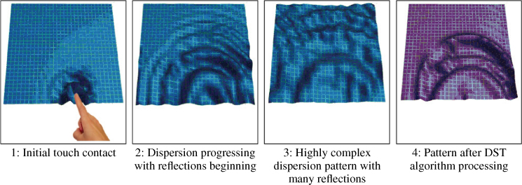
Figure 2.23 This figure is a graphic representation of the effect of bending waves on a glass substrate. The third graphic is typical of a pattern that APR would sample and compare offline; the fourth graphic is the result of processing the pattern through DST's real-time algorithms.
Source: Adapted from 3M Touch Systems.
As noted in the description of APR, the transmission velocity of bending waves through the substrate changes with frequency, causing the signal to be dispersed or spread. Upon receiving the signal, DST's approach is to re-integrate the spread signal by applying processing that allows for the differences in delay vs. frequency, then applying correlation processing between the four sensors before ultimately triangulating the original touch co-ordinates. In effect, it is a form of spread-spectrum technique, which is inherently tolerant of signal reflections and interference [42].
NXT PLC (New Transducers Ltd.) in the UK licensed their DST core technology exclusively to 3M Touch Systems in 2003. NXT (which renamed itself as HiWave Technologies PLC in 2010, and then again as Redux Labs in 2013), is known as the creator of the first flat-panel loudspeaker. In this device, piezoelectric transducers mounted on the periphery of a rigid substrate are driven with an audio signal, causing the substrate to function as a speaker diaphragm. NXT had realized (and patented) the reverse idea, that vibrations (bending waves) in the substrate could be sensed by the transducers and used to locate the source of the waves (the touch location).
3M Touch Systems and NXT did a substantial amount of joint development to commercialize DST technology, with 3M pre-announcing their first DST product in 2004 and actually launching the product in 2006. The initial launch was not successful; 3M Touch Systems withdrew the first product from the market for more than a year, finally re-launching it in 2007. Since 3M Touch Systems' bread-and-butter product at the time was surface-capacitive touchscreens in sizes from 5.7 to 32 inches, 3M Touch Systems targeted DST at large-format displays between 32 and 55 inches in order to avoid cannibalizing any of their surface-capacitive business. In contrast, Elo Touch Solutions focused on sizes under 32 inches – not for competitive reasons, but because they were unable to make APR perform well enough in digital signage applications (Elo's APR-based digital-signage products were withdrawn from the market in 2012).
Applications of DST are similar to those for camera-based optical and traditional infrared; interactive information and digital signage are the primary focus. DST has most of the same basic limitations as APR, summarized in Table 2.10.
Around the end of 2011, 3M Touch Systems stopped all further development on DST. Without further development, the technology will eventually become uncompetitive. Although 3M Touch Systems is currently continuing to sell DST into existing interactive information and digital-signage applications, it is likely that the technology will disappear from the market within five years.
2.7 Optical Touch Technologies
2.7.1 Traditional Infrared (#9)
The first widely recognized example of an infrared touchscreen appeared in 1972 in the PLATO IV educational system at the University of Illinois [43]. In this system, a 16-by-16 grid infrared touchscreen was overlaid on an orange plasma bit-mapped display in order to provide finger-selectable functions. One of the first commercial implementations of an infrared touchscreen was in 1983 in the HP-150, HP's first touch microcomputer (it had a nine-inch CRT and ran the CP/M operating system) [44]. During the 1980s and 1990s, Carroll Touch was considered to be the leading supplier of infrared touchscreens. AMP acquired Carroll Touch in 1984. In 1999, Tyco International acquired AMP and then later the same year acquired Raychem, who had acquired Elo Touch Solutions (Elographics) in 1986. In this way, Carroll Touch became part of Elo Touch Solutions in 1999.
As illustrated in Figure 2.24, a traditional infrared touchscreen has IR LEDs along two adjacent sides of the screen and IR photo-detectors along the other two sides. Each IR LED is pulsed in sequence, emitting light that is received by the opposing photo-detectors (the sequenced pulsing is why this technology is sometimes called “scanning infrared”). A grid of IR light beams in the X and Y directions is therefore formed just above the surface of the screen. When a finger or any IR-opaque object breaks the beams, a controller calculates the location of the touch.
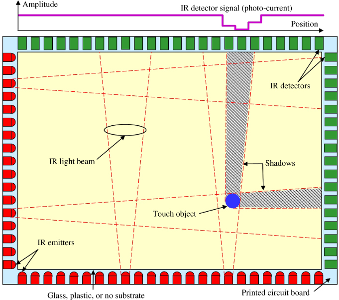
Figure 2.24 A traditional infrared touch sensor consists of a frame with infrared LEDs on two adjacent sides and infrared photo-detectors on the two opposite sides. The LEDs create a grid of infrared light; a touch is recognized when an infrared-opaque object blocks the light beams. Adapted from Elo Touch Solutions.
A minor but significant enhancement to infrared that was invented in the early 1990s by Elo Touch Solutions was the concept of “one transmitter, multiple receivers”. Instead of establishing a one-to-one correspondence between transmitting and receiving elements, each transmitting LED is seen by up to five receivers. This increases the robustness of the touch system, since a receiver can become disabled without creating a dead spot in the touchscreen. A related enhancement was the concept of checking for stationary objects and ignoring them if nothing had changed in several minutes. This prevents contaminants (e.g., a glob of peanut butter) from creating a dead spot on the touchscreen; the use of multiple receivers allows the contamination to be “looked around”, thus minimizing its effect. The term “traditional” is often used to indicate that the referred-to form of infrared is fundamentally the same as it was in the 1990s. Several newer forms of infrared have recently been developed; these will be discussed later in this section.
Infrared has the smallest market share of any of the mainstream touch technologies discussed so far; according to DisplaySearch, the total market size in 2012 was around $40M [12]. Almost all of this was in commercial applications, including ATMs, point-of-sale terminals, various kinds of kiosks, and large-format displays such as interactive digital signs and wayfinding stations. Infrared is one of the most robust touch technologies, capable of withstanding severe environments – for example, it can withstand direct sunlight and can be sealed against contaminants. For this reason, it is often used in outdoor touch applications. Infrared is also unique because it does not actually need any substrate at all – the IR light beams can be positioned directly above the display with no intervening glass. In that situation, the term “infrared touch-frame” is typically used instead of “infrared touchscreen”.
In most applications other than large-format, infrared is used: (a) because the device OEM has used it for a long time and believes that it is the best technology for his market (e.g., IBM in point-of-sales applications); or (b) because of its environmental capabilities. These reasons suggest that infrared is relatively unlikely to be replaced by p-cap. In indoor large-format applications, however, infrared is facing significant competition from camera-based optical, due to the lower cost of the latter, particularly for very large displays.
Infrared was originally a single-touch technology; when multi-touch became important, the major suppliers all started supporting some degree of two-touch. Because there are only two available axes of information (X and Y), two touches can not be uniquely resolved without additional information (this is the same problem as ghost touches in self-capacitive). This limited degree of multi-touch support is sometimes called “1.5 touches”. In the late 2000s, Elo Touch Solutions developed a clever method of adding a third axis of information using diagonal light beams (they called the additional dimension “U”) [45]. This allowed the resolution of two touches most of the time, except for the special case when the two touches were exactly in line with the diagonal beams (occluding each other). Unfortunately, Elo Touch Solutions never put the technology into mass production due to its high cost.
Traditional infrared is likely to continue to exist as a unique technology, particularly in applications where environmental resistance is critical. Market share in small-to-medium sizes is likely to remain relatively constant during the next five years, while market share in large format is likely to decline due to the growth of camera-based optical.
The advantages and disadvantages of traditional infrared touch technology are listed in Table 2.11.
Table 2.11 Advantages and disadvantages of traditional infrared touch technology
| Traditional infrared advantages | Traditional infrared disadvantages |
| Scalable to very large sizes (over 100 inches) | Mostly single-touch; limited support for two touches (“1.5 touches”) |
| Activation by any IR-opaque object with zero touch force | Pre-touch (touch activation before actually contacting the surface of the screen) |
| High optical performance due to plain glass substrate | Profile height (IR emitters and receivers project above the touch surface); printed circuit board (PCB) must totally surround screen |
| Easy to integrate; available with or without a substrate; even available as build-it-yourself frame segments | Bezel must be designed to include an IR-transparent window |
| Very durable; can be vandal-proofed with tempered or chemically strengthened (CS) glass | Extremely difficult to prevent false touches (from shirtsleeves, insects, etc.) |
| Can easily be environmentally sealed for use outdoors | Relatively low resolution and accuracy |
| Can be made immune to interference from high levels of ambient IR (e.g., 75K lux) | Minimum touch-object size typically |
| Relatively high cost compared with camera- based optical (scales as a function of perimeter) |
2.7.1.1 Waveguide Infrared
Beginning around 2000, an Australian startup named RPO began developing polymer optical waveguides targeted at the “last mile” telecommunications market. When the “last mile” market collapsed in 2002 because of extreme overexpansion of fiber, RPO regrouped and looked for a new application. In 2004, they decided to use the optical waveguides they had developed in a variation of traditional IR touchscreens [46]. They named their technology Digital Waveguide Touch ![]() . As illustrated in Figure 2.25, their concept was to use a single light source with two sets of optical waveguides transmitting the light in the X and Y directions, with a second pair of waveguides collecting the light and guiding it into a single multi-pixel photo-detector. The waveguides were produced on fabrication (“fab”) equipment similar to that for LCDs using photolithography; this allows very high resolution, so the waveguide channels could be as small as
. As illustrated in Figure 2.25, their concept was to use a single light source with two sets of optical waveguides transmitting the light in the X and Y directions, with a second pair of waveguides collecting the light and guiding it into a single multi-pixel photo-detector. The waveguides were produced on fabrication (“fab”) equipment similar to that for LCDs using photolithography; this allows very high resolution, so the waveguide channels could be as small as ![]() each.
each.
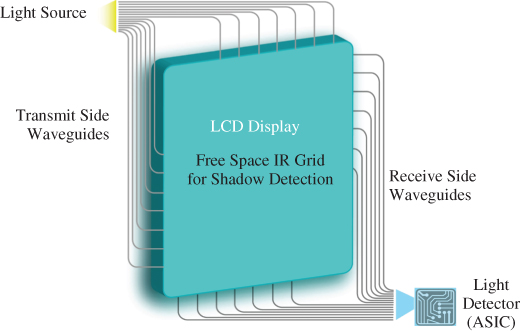
Figure 2.25 Conceptual diagram of RPO's waveguide-infrared touch technology.
Source: RPO.
As often happens, the difficulty and restrictions of implementing the concept in the real world resulted in a somewhat more complex design, shown in Figure 2.26.
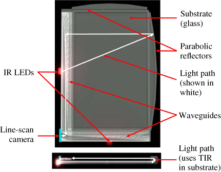
Figure 2.26 RPO's actual construction of a 3.5-inch waveguide-infrared touchscreen.
Source: Photo by RPO; annotation and arrows by the author.
Constrained by limited border space, RPO used only a single pair of waveguides to collect the light and guide it into the receiving photo-detector (a line-scan CMOS sensor containing ![]() pixels each for X and Y). In order to distribute the light across the substrate, RPO used two lensed IR-LEDs, one for X and one for Y. The substrate itself was used as an optical waveguide (making use of total internal reflection (TIR)), and a parabolic reflector in the opposite two sides made a 180° change in the direction of the light and helped spread the light out across the substrate. The white lines in Figure 2.26 show the path of one light ray from the LED on the left side of the touchscreen into the optical sensor, in both a top view and an edge view. The result was a low-cost, high-performing IR touchscreen optimized for the 3-inch to 15-inch (mobile) size range [47].
pixels each for X and Y). In order to distribute the light across the substrate, RPO used two lensed IR-LEDs, one for X and one for Y. The substrate itself was used as an optical waveguide (making use of total internal reflection (TIR)), and a parabolic reflector in the opposite two sides made a 180° change in the direction of the light and helped spread the light out across the substrate. The white lines in Figure 2.26 show the path of one light ray from the LED on the left side of the touchscreen into the optical sensor, in both a top view and an edge view. The result was a low-cost, high-performing IR touchscreen optimized for the 3-inch to 15-inch (mobile) size range [47].
Where the technology fits best is on devices with reflective screens (e.g., e-readers that use E-ink's electrophoretic display). IR's ability to operate without any additional layers on top of the screen is an excellent match with a reflective screen's need to effectively use every photon of light that is available (RPO's glass substrate, a form of waveguide, can be placed underneath the e-reader display). However, like all touch technologies, waveguide infrared has some fundamental limitations in this application, as follows:
- Multi-touch is limited to two touches because there are only two sources of positional information; ghost touches are minimized in firmware, but not completely eliminated.
- A bezel is required to protect the waveguides and reflectors. Total height is only about 1.5mm, but it is still not zero, like the bezel on today's smartphones and tablets.
- The technology is relatively sensitive to debris on the screen, because the waveguide channels are only
 above the surface.
RPO announced the technology in 2007, showed improved performance in 2008, showed larger sizes in 2009, and showed the technology working in a 13.3 inch notebook in 2010 – all at the Society for Information Display's (SID's) Display Week conferences. RPO was counting on a partnership with a very large LCD/consumer–electronics manufacturer (one big customer). When the partnership suddenly derailed at the end of 2010, RPO was not sufficiently prepared with an alternative source of funding to support the manufacturing ramp required by the consumer-electronics market. After a total of $55M investment over more than ten years, RPO went into liquidation in 2011. The sale of the assets (patents) took place in 2012. It is unclear if this technology will ever be put to productive use again.
There is one further historical aspect to this technology that is worth mentioning. A very similar waveguide-infrared touch technology was invented and patented, well before RPO even started thinking about theirs, by Poa Sana (Swahili for “very cool”), a startup located in Silicon Valley, California. Poa Sana's first patent was filed in 1997 and issued in 1999 [48]. Between 1997 and 2002, Poa Sana made little progress towards commercialization of the technology, spending most of the $3.5M they raised on R&D. In 2003, National Semiconductor, which was at the time exploring entering the touchscreen market, acquired the rights to Poa Sana's IP. After spending several years working with the technology and assessing market opportunities for it, National Semiconductor concluded that the future of the technology was not bright enough, so they gave Poa Sana's IP back to its founders. There were never any lawsuits filed between RPO and Poa Sana, because there was never enough revenue produced by either company to justify a lawsuit.
There are probably three basic reasons why waveguide infrared technology failed at the time that it did, as follows:
- The application for which the technology was best (e-readers and other products with reflective displays) was still a fairly small niche market in 2010 (Remember, “everything is best for something and worst for something else” [5]. Any technology must excel in at least one application in order to be successful).
- The fundamental nature of the technology could not support true multi-touch and bezel-less designs, both of which became essential for consumer electronics products after the introduction of the iPhone in 2007.
- The waveguide technology limited the touchscreen size to less than about 14 inches, preventing its application in many other potential markets.
Any technology has an optimum time and place, so it may be that waveguide infrared's time just has not come yet. At least one company (Nitto Denko) has filed and/or received recent patents in this technology area, so it may not be totally dead.
2.7.2 Multi-touch Infrared (#10)
Multi-touch infrared touch-technology is based on a new “imaging” method of using essentially the same physical IR LED emitters and photo-detector receivers that are present in traditional infrared touchscreens. The new method supports up to ![]() simultaneous finger-touches; the main difference is in how the controller manages the emitters and receivers. Instead of simply looking for pairs of interrupted light beams, the controller in most implementations of this new technology uses as many of the available receivers as possible to capture the shadows of all objects touching the screen created by each individual IR emitter.
simultaneous finger-touches; the main difference is in how the controller manages the emitters and receivers. Instead of simply looking for pairs of interrupted light beams, the controller in most implementations of this new technology uses as many of the available receivers as possible to capture the shadows of all objects touching the screen created by each individual IR emitter.
There are three different arrangements of IR emitters and detectors that are used in this imaging method. The first two are identified by their creator: (A) PQ Labs, who invented the category and launched their first product in January 2009, and (B) Image Display Systems; the third arrangement (C) cannot be attributed to a specific creator at this time.
As illustrated in Figure 2.27A, B and C, one IR LED emitter flashes, and many or all of the IR photo-detectors on the two opposite sides record their level of light intensity, producing a one-pixel-high “image” showing the shadows of all the objects between the emitting LED and the photo-detectors. Each pixel in the image (i.e., data from a specific photo-detector) typically is rendered in a gray-scale, which is useful in delineating the edges of moving objects, since real-world shadows do not have sharp edges when the object is moving. Each time an IR LED flashes, the “image-capture” process is repeated. Doing this extremely rapidly and then combining the image sequences in a mathematical array [49] allows a relatively large number of shadow-creating objects to be tracked simultaneously.
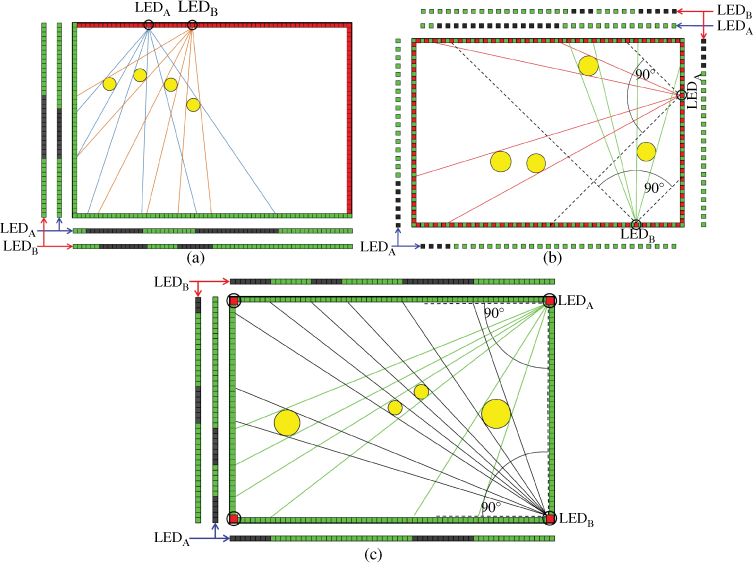
Figure 2.27 Multi-Touch Infrared touch-screens typically use an “imaging” approach. There are currently three different architectures: 28A by PQ Labs, 28B by Image Display Systems  , and 28C by unknown. The architectures are similar, in that each IR LED emitter flashes, and many or all of the IR photo-detectors on two or three opposite sides record their level of light intensity, producing a one-pixel-high “image” showing the shadows of all the objects between the LED and the photo-detectors.
The hardware used in all three architectures is relatively similar. The difference in the user experience produced by different multi-touch infrared products is determined mostly by the quality of the algorithms used to interpret the “shadow-image” data, reject ghost-points, handle occlusion, and track moving and non-moving objects.
There are only a few suppliers of this technology so far; the best-known ones are PQ Labs (the creator of the category), Citron (![]() brand), Image Display System (
brand), Image Display System (![]() brand), TimeLink, and ZaagTech.
brand), TimeLink, and ZaagTech.
Two key characteristics of this technology's use of resources are the need for very high-speed sequencing and a large amount of continuous image processing. Because the maximum resolution of which this technology is capable is related to the spacing between the IR photo-detectors (generally spaced on 5 mm centers), line-drawing with this type of touchscreen can show evidence of “stair-stepping” or “jaggies”. Also, as the touch objects get larger or closer to the IR LEDs, their shadows become larger which, in effect, reduces the amount of data that each image is capable of holding.
Oddly, the primary problem with this technology is the lack of a clear application. This technology seems to be driven more by mainstream enthusiasm about multi-touch than by any actual application need. Current commercial infrared touchscreen applications rarely need more than two touches, and nobody has defined any real applications for 20–40 touches. Another impediment is that the problem of identifying which touch belongs to which user does not yet have an elegant (practical) solution. Multi-player games on large horizontal displays (gaming tables) are probably the best opportunity for multi-touch infrared, but it is not clear that this technology is fast enough or has enough resolution for that application. Large displays used in multi-person gaming in casinos today (e.g., roulette) typically use wire-based p-cap because it is fast, the touchscreen surface can be made flush, it is unaffected by light-blocking objects on the surface, and it is readily available from suppliers such as Zytronic [50].
Multi-touch infrared technology is not very suitable for interactive whiteboard applications because of inadequate resolution, slow speed and large minimum touch-object size. Interactive whiteboard applications generally require a stylus and very rapid recognition of the stylus being lifted (“pen-up”) by less than one millimeter. It is very difficult to meet the pen-up requirement with any form of infrared in which the IR emitters are positioned above the surface of the screen. While there are implementations of multi-touch infrared technology in interactive whiteboard products (particularly from Asian competitors of PQ Labs), the resulting user experience is generally unsatisfactory.
The advantages and disadvantages of multi-touch infrared touch technology are listed in Table 2.12.
Table 2.12 Advantages and disadvantages of multi-touch infrared touch technology
| Multi-touch infrared advantages | Multi-touch infrared disadvantages |
| Scalable multi-touch from 2 to |
No clear application for a high number of touches in the large-format market |
| Most of the same advantages as traditional infrared (scalable size, broad activation, zero touch force, high optical performance, durable, sealable) | Most of the same disadvantages as traditional infrared (pre-touch, profile height, PCB surround, bezel design-complexity, false touches, low resolution and accuracy; minimum touch-object size) |
| Object-size recognition (a by-product of the imaging method that captures a view of each object from multiple vantage points) | Performance is often not as good as traditional infrared (slower response, stair-stepped lines, more jitter, etc.) |
| More difficult to make immune from high levels of ambient IR, which makes it less useful outdoors | |
| Disproportionately higher cost than traditional infrared (may be due to temporary “market pricing”) |
The current status of multi-touch infrared touch technology can be best assessed by visiting the website of PQ Labs (the clear leader of the category). At the time this book is being written in 2013, the website's Demo page [51] includes seven videos averaging 2.5 minutes each; in all of those 18 minutes of video, there are almost no applications shown that use more than two touches. The most compelling application shown is an air-hockey game with two players, each using two paddles.
On the other hand, further study of the PQ Labs website reveals marketing claims regarding the elimination of many of the disadvantages of the technology category. For example, they claim that they distribute the controller processing load by adding up to 10 “Light Processors” (some undefined form of CPU) that execute most of the multi-touch processing in the touchscreen frame, thus optimizing touch speed and accuracy. PQ Labs claims a minimum touch-object size of only 1.5 mm (compared with the typical ![]() specification) – except that the claim does not appear in the product specifications, only in the marketing description of the product. PQ Labs claims to have “optimized handwriting algorithms and a unique Whiteboard Mode” which allows their products to support clear writing of complex graphics such as mathematical formulas. They claim immunity to “bow and twist” and immunity to “adverse lighting conditions” – without providing either a “minimum planarity requirement” specification or a “maximum ambient IR lux” specification.
specification) – except that the claim does not appear in the product specifications, only in the marketing description of the product. PQ Labs claims to have “optimized handwriting algorithms and a unique Whiteboard Mode” which allows their products to support clear writing of complex graphics such as mathematical formulas. They claim immunity to “bow and twist” and immunity to “adverse lighting conditions” – without providing either a “minimum planarity requirement” specification or a “maximum ambient IR lux” specification.
The above paragraph provides an excellent illustration and example of one of the fundamental problems that occurs throughout the touch industry – insufficient specifications with an excess of marketing claims.
2.7.3 Camera-based Optical (#11)
Although camera-based optical touch only came to prominence in 2009 with the launch of Windows 7, the technology has existed for more than 30 years. In 1979, Sperry Rand Corp. was the first to patent the concept of using two infrared linear image sensors (they were charge-coupled devices (CCDs) at the time) to locate the position of a touch on the top surface of a display. SMART Technologies in Canada and NextWindow in New Zealand both developed the first commercial complementary metal-oxide-semiconductor (CMOS) based optical touch systems independently in the early 2000s. SMART used the technology in a few of their products during the 2000s, but did not start making significant use of it until 2010.
Hewlett-Packard was the first to use optical touch in a desktop product, launching the ![]() consumer all-in-one computer in 2007 with NextWindow's touch technology. SMART filed a lawsuit against NextWindow for patent infringement in April of 2009 and then licensed their camera-based optical technology to Pixart in June of 2009. Pixart immediately began supplying optical sensors to Quanta for the launch of Windows 7 in October 2009; Quanta became NextWindow's primary competitor. SMART acquired NextWindow in April of 2010, thus ending the lawsuit and lessening the financial impact of Quanta as a competitor. Combining the optical-touch IP of both companies made more sense than the possibility of one company invalidating one or more of the other's patents as a probable outcome of the lawsuit.
consumer all-in-one computer in 2007 with NextWindow's touch technology. SMART filed a lawsuit against NextWindow for patent infringement in April of 2009 and then licensed their camera-based optical technology to Pixart in June of 2009. Pixart immediately began supplying optical sensors to Quanta for the launch of Windows 7 in October 2009; Quanta became NextWindow's primary competitor. SMART acquired NextWindow in April of 2010, thus ending the lawsuit and lessening the financial impact of Quanta as a competitor. Combining the optical-touch IP of both companies made more sense than the possibility of one company invalidating one or more of the other's patents as a probable outcome of the lawsuit.
Camera-based optical is a form of light-blocking IR touch (“camera” here refers to an assembly that typically includes an image sensor, a lens, an IR filter, a housing and a cable). In the most common form of camera-based optical touchscreen (illustrated in Figure 2.28A), a peripheral backlight is provided via IR LEDs in the corners of the screen, with a retro-reflector around the periphery of the screen (a retro-reflector is a material that returns light in the direction from which it came, regardless of the angle of incidence). As a result of the retro-reflectors, light is radiated from the edges of the screen across the surface of the screen. CMOS line-scan or area imagers (cameras) are placed in two or more corners of the screen; when a finger touches the screen, the peripheral light is blocked and a shadow is seen by the cameras.
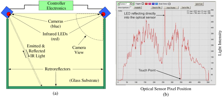
Figure 2.28 Camera-based optical touch uses a backlight created by IR LEDs in the corners of the screen and a peripheral retro-reflector. CMOS line-scan sensors (cameras) are placed in two or more corners of the screen; when an IR-opaque object touches the screen, the peripheral light is blocked and a shadow is seen by the cameras.
Source: Adapted from NextWindow.
Note that even if the camera uses an area imager rather than a one-pixel-high line-scan imager, it is not seeing a grey-scale image of the touching finger; it is simply seeing the presence or absence of light. A controller processes the data from the cameras and uses triangulation to determine the location of the touching finger [52].
Figure 2.29B shows a graph of light intensity seen by one 512-pixel optical sensor. The sharp dip in the graph at pixel 358 is the result of a touch on the screen (i.e., a point where all of the peripheral backlight is blocked). The moderate dip around pixel 250 is the junction of the two edges of the screen (i.e., the bottom and right-hand edges, as seen by a camera in the upper left corner); this is the most distant point from the camera. The sharp peak around pixel 270 is the one point where the retro-reflector is sending light directly back into the camera.
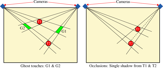
Figure 2.29 Ghost touches (G1 and G2, shown in green on the left) and occlusions (a single shadow from touch-objects T1 and T2 on the right) become a problem when trying to uniquely identify two touches in a two-camera optical touchscreen because there are not enough sources of positional data.
The majority of camera-based optical touchscreens used in desktop products in 2009–2012 had only two CMOS sensors, mainly for cost reasons. Using triangulation, two cameras are required in order to calculate the X and Y locations of a single touch point. If two simultaneous touch points can be seen by both cameras (i.e., each camera sees two distinct shadows), then there are four potential touch points – two real touch points and two “ghost” points (false touches positionally related to real touches). This is the same problem that exists with self-capacitive p-cap, traditional IR and single-touch SAW – all touch systems where information can be obtained only from two axes. Distinguishing real points from ghost points in optical touch requires the application of sophisticated algorithms operating on multiple sets of points over time.
Another situation in which advanced algorithms is important is when the position of the two simultaneous points is such that one of the cameras cannot distinguish between them (i.e., one touch-point occludes the other). Figure 2.29 A & B illustrates both ghost points and occlusion.
Much of an optical touchscreen's controller processing time in a two-camera optical touch system is used running algorithms to eliminate ghost points and compensate for occlusion. In fact, the quality of the multi-touch experience in a two-camera optical touch system depends largely on the sophistication of the algorithms, not the quality of the hardware. For these reasons, some large format ![]() optical touchscreens use four cameras to provide more data sources. Four cameras can provide two unambiguous touches, except for one special case, where both touches are on one of the diagonals between the cameras, such that both cameras see an occluded view.
optical touchscreens use four cameras to provide more data sources. Four cameras can provide two unambiguous touches, except for one special case, where both touches are on one of the diagonals between the cameras, such that both cameras see an occluded view.
The above paragraphs describe a system where the backlight is created by light from IR LEDs in the corners of the screen reflected by a peripheral retro-reflector. This is called a “passive” backlight system, since the shadows sensed by the cameras are created by reflected light. The backlight can also be “active” – that is, it can directly emit light. There are generally two methods of constructing an active backlight. In the first, more common method, a large number of IR-emitting LEDs are located around the periphery of the touchscreen, and these directly emit light that is blocked by a touch-object. The primary advantage of this method is that the higher-intensity light produces a higher touch-system signal-to-noise ratio, which increases the robustness of the touch function. The primary disadvantages of this method are the added cost of the components and the surrounding printed circuit board.
In the second method (used only by Lumio due to IP considerations), tubular light-guides around the periphery of the screen redirect IR light produced by an LED at each end of a waveguide segment, so that it spreads out across the surface of the screen. The primary advantages of this method are lower cost and much lower profile height (3–4 mm versus 6–10 mm); the primary disadvantages are lower light intensity and its single-source nature.
Applications for camera-based optical touch in 2013 were in two main areas:
- desktop all-in-one touch computers and touch monitors;
- large format interactive information, digital signage, conference and training rooms, and large interactive LCDs replacing whiteboards in some educational applications.
The desktop application area developed mainly because Microsoft's Windows 7 Touch Logo specification was written around the capabilities of camera-based optical, which at the time was the lowest-cost technology capable of supporting two touches. The Windows 8 Touch Logo specification is written around p-cap, with a minimum requirement of five simultaneous touches. NextWindow has been able to meet the Windows 8 Touch Logo specification by using six cameras – one in each corner, with two additional cameras trisecting the top edge of the screen. At the present time, no other camera-based optical suppliers (other than SMART Technologies, NextWindow's parent, which only sells complete systems and not touchscreens) have announced products that meet the Windows 8 Touch Logo specification.
Because of the high cost of p-cap in desktop (15 to 30 inch) sizes, camera-based optical is seen as a desirable alternative for Windows 8 consumer products. However, PC OEM/ODMs generally prefer to have multiple sources so, until suppliers other than NextWindow emerge, penetration of camera-based optical in Windows 8 desktop products will be limited.
The primary competition for camera-based optical in large-format applications is traditional IR; secondary competition comes from wire-based p-cap, SAW, and Dispersive Signal Technology (DST) from 3M (the latter two technologies are limited to a maximum size of about 52 inches). Camera-based optical's primary advantage over traditional IR is its scalability, which translates into lower cost for larger touchscreens. A traditional IR touchscreen of any size must have a printed circuit board completely surrounding the screen, while a camera-based optical touchscreen can use printed retroreflectors which can be attached to a plastic or metal bracket. The latter is much lower in cost. A secondary advantage of camera-based optical over traditional IR is higher resolution and speed.
In large format applications, both optical touch and traditional IR have individual strengths, so it is likely that both will continue to exist in the large format market for a number of years. Over time, camera-based optical will overtake traditional IR because the hardware is simpler and more capability can be added through software. The advantages and disadvantages of camera-based optical touch technology are shown in Table 2.13 below.
Table 2.13 Advantages and disadvantages of camera-based optical touch technology
| Camera-based optical advantages | Camera-based optical disadvantages |
| Scalable to very large sizes (up to 120 inches) | Profile height (camera modules project above the touch surface); increases with larger screens |
| Activation by any IR-opaque object with zero touch force (stylus independence) | Pre-touch (touch activation before actually contacting the surface of the screen), but less severe than traditional IR |
| Multi-touch (2–5 touches is typical, but 40 touches has been achieved using 20 cameras) | Relatively high degree of substrate planarity (e.g., |
| Relatively high resolution and accuracy, sufficient to meet the Win8 requirements | Extremely difficult to prevent false touches (from shirtsleeves, insects, debris on the screen, etc.) |
| Object-size recognition (a byproduct of capturing a view of each touch-object from multiple vantage points) | Multi-touch capability is inherently lower than p-cap due to many fewer data sources; two-touch performance with two cameras is very weak |
| High optical performance due to plain-glass substrate | Accuracy is non-uniform across screen, especially with only two cameras |
| Lower cost than traditional or multi-touch IR | Minimum touch-object size depends on screen size; can be as large as 7 mm for very large screens |
| Available with or without glass substrate | More sensitive to ambient IR than traditional IR (less-developed solutions) |
| Side-by-side screens can interfere with each other due to IR light from one being detected by the other |
2.7.3.1 PIN-Diode Optical
PIN-diode optical is a variation of camera-based optical that is currently available only from Baanto due to IP considerations. This optical touch-technology uses PIN diodes (diodes with a p-i-n semiconductor structure) as light sensors, instead of CMOS cameras, as described above. PIN diodes have the following characteristics which simplify the structure of an optical touchscreen [53]:
- PIN diodes directly read light intensity and operate at up to 10,000 frames per second, which supports very high-performance touch systems.
- PIN diodes do not require a lens and can be configured with a field-of-view (FOV) approaching 180 degrees (see Figure 2.30), which eliminates reliance on sensors placed in the corners of a touchscreen and eliminates optical aberrations that require computational correction.
- PIN diodes do not require exposure control, since sensor performance is not affected by illumination changes due to the distance or velocity of a touch-object.
- PIN diodes have an infinite depth of field, which means that position-detection algorithms do not change with the position of a touch-object.
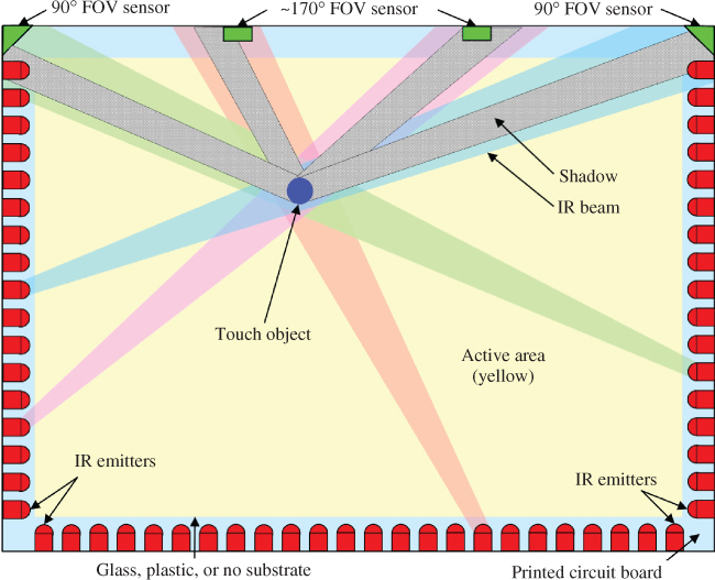
Figure 2.30 An example of a PIN-diode optical touchscreen, which uses two 90° field-of-view (FOV) sensors in the corners, and two 170° FOV sensors along the top edge. The other three edges of the touchscreen contain IR LEDs. The light rays are drawn to illustrate that a sensor may see both the shadow of a touch-object and the peripheral light, depending on the size of the touch-object.
Source: Adapted from Baanto.
PIN diodes operate entirely in the analog domain, which allows the touchscreen controller to use the information about the shadows created by touch-objects in a different manner than more digitally-oriented image processing technology (Baanto's technology is branded ![]() ). Some of the capabilities that this enables, and which are not generally found in other types of camera-based optical touchscreens, include the following [54]:
). Some of the capabilities that this enables, and which are not generally found in other types of camera-based optical touchscreens, include the following [54]:
- Selectable touch-area (for providing palm-rejection, ignoring rain drops on the screen, or setting the minimum required finger-pressure).
- Selectable “dwell time” (minimum number of frames a touch-object must be present before reporting a valid touch event, which allows rejecting brief accidental touches).
- Selectable shadow density (allows the infrared opacity of the touch-object to become a criterion in declaring a valid touch).
- Greater ability to reject high levels of ambient infrared (up to 100K lux).
- Easier scaling to very large sizes (Baanto's largest touchscreen to date is on a 266-inch video wall).
The backlight for Baanto's PIN-diode optical touchscreens is active, utilizing 940 nm IR LEDs spaced on 5 mm centers around the periphery of the touchscreen. The touchscreen's use of the ratio between fully illuminated, partially shadowed, and fully shadowed touch-events makes the touchscreen tolerant of different LED power levels around the periphery, eliminating the need to use “binned” (matched) LEDs. Also, since the controller algorithms use the ratio between readings, changes in the total power received by the sensors do not impact the position calculation.
2.7.4 In-glass Optical (Planar Scatter Detection – PSD) (#12)
Planar Scatter Detection (PSD) is a unique form of in-glass optical touch invented at FlatFrog, a startup founded in early 2007 in Sweden that shipped its first product in May 2012. The core of FlatFrog's touch technology could be termed “optical waveguide analysis”. The “waveguide” is the touch substrate, which can be any dimensionally stable transparent material. It does not have to be rigid or flat, which is a very unusual characteristic for an optical touch system. The basic functionality of FlatFrog's system is shown in Figure 2.31. In a PSD touch-sensor, light is injected into the edges of an optical substrate by multiple IR LEDs and remains confined inside the substrate by total internal reflection (TIR). A touch scatters a portion of the light due to frustrated total internal reflection (FTIR); multiple IR photo-detectors, interleaved with the LEDs on the edges of the substrate, detect the remaining (reduced-intensity) TIR light. Complex algorithms determine the location of all objects on the surface by analyzing the light-ray intensities and doing a one-dimension to two-dimension (1D-to-2D) reconstruction [55].
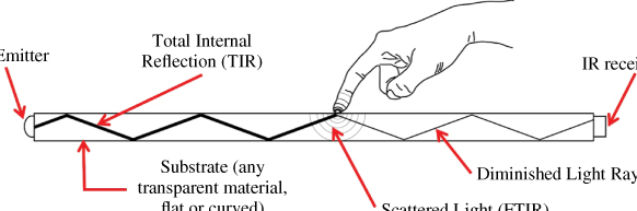
Figure 2.31 This figure is a schematic illustration of the Planar Scatter Detection principle. IR light is injected into the substrate (waveguide); it stays confined in the substrate due to TIR. A touch scatters some of a light ray due to FTIR; the reduced-intensity ray continues until it is detected at the opposite edge of the substrate by a photo-detector. Sophisticated algorithms calculate the location of the touch by analyzing all the light-ray intensities.
Source: Adapted from FlatFrog.
One of the aspects that make PSD different from standard FTIR is that the light resulting from FTIR is analyzed within the substrate; it does not have to escape, as in vision-based touch. Another is that a touch only consumes a small amount of a given light ray, so that multiple touches can be located in a straight line with enough light left over to be still sensed at the edge. Like traditional IR, PSD requires a circuit board on all four edges of the substrate, but the number of IR emitters and receivers is slightly less than required for a traditional IR touchscreen (7–8 mm component spacing versus 5 mm spacing). Unlike traditional IR, a PSD touchscreen has a totally flush bezel, since nothing projects above the surface of the display.
The only product incorporating PSD that is currently shipping in 2013 is a 32-inch LCD touch-display assembly from FlatFrog. In other words, at the present time, this touch technology is not available as a component. However, Intel Capital has invested in FlatFrog, and Intel is working directly with FlatFrog on the commercialization of the technology as a component. It is likely that by 2014, PSD touch-technology will be available as a component for all-in-one computer (e.g., 23-inch) displays. FlatFrog intends to use a licensing business model in high-volume consumer electronics applications, and a product-sales business model in low-volume commercial large-format applications. PSD may be able to offer some serious competition for traditional IR and camera-based optical in large-format, and potentially even for p-cap starting from laptop-size and up. The advantages and disadvantages of PSD touch-technology are listed in Table 2.14.
Table 2.14 Advantages and disadvantages of in-glass optical (PSD) touch technology
| In-glass optical (PSD) advantages | In-glass optical (PSD) disadvantages |
| Very robust multi-touch ( |
IR emitters and receivers require printed circuit board around perimeter (9 mm wide), plus one driver ASIC per 12 pairs of components |
| Edge-to-edge (bezel-less) or with bezel (like p-cap) | Cannot meet Windows pen-digitizer interface specifications due to lack of hover, so not optimum for stylus applications |
| Practical size range is 14–84 inches (better than p-cap) | False touches are possible from soft objects that cause FTIR |
| High resolution (400 dpi) and accuracy, sufficient to meet the Win8 requirements (like p-cap) | Sensitive to ambient IR (may be improved in future); dust or smoke on touch surface can affect performance due to change in FTIR |
| High optical performance due to plain glass or plastic substrate (better than p-cap) | Emerging touch-technology; cost-competitiveness and volume product capability are still to be proven |
| Very light touch (similar to p-cap); 10 bits of pressure-sensitivity due to changes in optical properties of finger as pressure increases (better than p-cap) | As of 2013, directly replacing p-cap requires more space (3 mm) between cover-glass and LCD and cannot be direct-bonded; direct bonding requires component PCB to be outside LCD frame, which increases display border-width |
| Works with finger, glove, passive soft-tip stylus (any soft object capable of causing FTIR) | |
| Insensitive to EMI/RFI (better than p-cap) | |
| Capable of operating at up to 1,000 Hz data rate (good for large screens, better than p-cap) | |
| Lower cost than p-cap in desktop sizes; driver ASICs and firmware/software are only unique components |
2.7.5 Vision-based Optical (#13)
Vision-based touch here refers to the use of “computer vision” to detect and process touch in contact with a surface. While the same term is also used (more commonly, perhaps) to describe the detection and processing of in-air gestures seen by 2D and/or 3D cameras, the latter technology is excluded from discussion in this chapter since it does not involve contact with a display. Computer vision also implies heavy use of image-analysis software to determine touch locations and other information about what is contacting the touch surface.
2.7.5.1 Projection
There are currently three methods of producing vision-based touch:
- projection;
- multiple wide-angle cameras behind an LCD; and
- light-sensing in-cell.
The projection method used in vision-based touch is usually rear projection, with a camera located next to the projector (as shown in Figure 2.32). Frustrated total internal reflection (FTIR, also illustrated in Figure 2.32) is the most commonly used method of producing “blobs” of IR light (bright luminescent objects) resulting from touches on the projection surface [56]. Microsoft Surface 1.0, launched in 2007 (and many of the similar “touch tables” that followed in the next four years) are the best examples of rear-projection vision-based touch. The primary advantage of this method is that a system can be assembled at very low cost [57]; the primary disadvantage is the physical size of a rear-projection system, plus the relatively low image quality that results from rear projection.
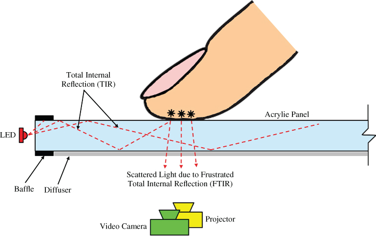
Figure 2.32 The most common method of producing vision-based touch utilizes rear projection with a camera located next to the projector. Frustrated total internal reflection is most commonly used to generate light resulting from touches on the projection surface.
Source: Adapted from Perceptive Pixel.
There are three other methods of supplying the light that produces the IR blobs in the projection method of vision-based touch:
- Diffused illumination (DI);
- laser light-plane (LLP); and
- diffused surface illumination (DSI) [58].
Diffused illumination refers to providing a uniform distribution of IR light across the underneath of the touch surface. This is usually achieved via one or more IR emitters located at some distance from the screen, and it is the method that was used in Microsoft Surface 1.0. Laser light-plane refers to using lasers to create a thin (1 mm) plane of IR light just above the touch surface; when a finger breaks the plane, an IR blob is produced. Typically, two or four lasers are used in the corners of the screen; a 120-degree line-filter is placed on each laser to spread out the laser beam. Diffused surface illumination uses a special acrylic to distribute the IR light evenly across the surface. The acrylic contains small reflective particles; when an IR LED shines its light into the edge of the acrylic, the particles redirect the light and spread it to the surface of the acrylic. The effect is similar to diffused illumination, but with more uniformity.
2.7.5.2 Integrated Cameras
The only current product that uses multiple wide-angle cameras integrated into an LCD to produce vision-based touch is ![]() from MultiTouch in Finland (see Figure 2.33). In this touch-display product, the cameras are integrated into the LCD's backlight. The primary advantages of this method are the relative thinness of the display (8 inches) compared with projection, and the high performance that can be achieved. The primary disadvantages are the cost, complexity, and thickness of the solution. Some of the more valuable characteristics of the MultiTaction product are as follows [59]:
from MultiTouch in Finland (see Figure 2.33). In this touch-display product, the cameras are integrated into the LCD's backlight. The primary advantages of this method are the relative thinness of the display (8 inches) compared with projection, and the high performance that can be achieved. The primary disadvantages are the cost, complexity, and thickness of the solution. Some of the more valuable characteristics of the MultiTaction product are as follows [59]:
- Immunity to external lighting conditions (achieved by reading both ambient light and the reflected light from the IR emitters embedded in the backlight).
- Unlimited number of touch points and users (the touchscreen software also identifies hands, not just touch points).
- Object recognition using 2D markers and/or generic shape-recognition.
- Operation with an IR-emitting stylus (creates clear differentiation between finger and stylus).
- Modular touch-displays can be formed into multi-user interactive walls.
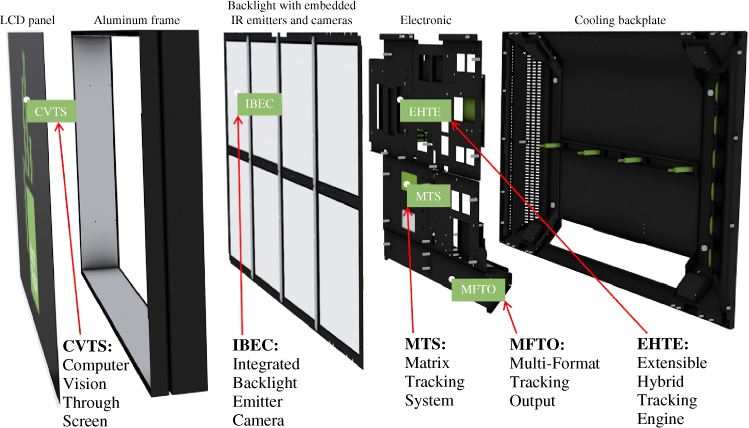
Figure 2.33 The MultiTaction vision-based touch system from MultiTouch in Finland uses IR emitters and IR cameras integrated into the backlight of a standard LCD, supported by sophisticated object-tracking software running on an embedded processor.
Source: Adapted from MultiTouch.
2.7.5.3 Embedded In-cell Light-sensing
The technology of embedded in-cell light-sensing is discussed in more detail in the Embedded Touch Technologies section that follows. The Samsung SUR40 touch-display that is used in Microsoft Surface 2.0 is the only current example of embedded in-cell light-sensing technology used to produce vision-based touch in a commercially available product (Surface 2.0 was launched in 2011 and renamed in 2012 as Microsoft PixelSense in order to make the “Surface” name available for use in consumer tablets). The primary advantage of embedded in-cell light-sensing is that touch is fully integrated into the display without adding any thickness. The key disadvantages of in-cell light-sensing (as implemented in the SUR40) are extreme sensitivity to ambient IR (such that the SUR40 cannot be used in most brightly lit environments [60]) and the increase in touch latency apparently caused by the time required to process the data from the embedded light sensors.
2.7.5.4 Vision-Based Summary
Applications for vision-based touch currently fall into two categories:
- A common platform for touch research in many universities due to the high multi-touch capability and low cost of self-fabrication [57]; and
- A new platform for traditional commercial applications, such as product-focused touch-tables in retail stores, and interactive video walls in public venues.
Although vision-based touch is still in its infancy, it is here to stay as at least a niche technology the primary reason beng that it is not directly competing with other touch technologies. The “vision” aspect of the technology allows it to do things that other touch technologies can not. One simple example is object recognition through the use of graphic tokens attached to objects [61]. This enables an application where (for example) a digital camera or smartphone with an attached token is placed on the touch surface and application software automatically downloads the photos from the device via Bluetooth and displays them for editing or arranging on the display – without the need for the user to give any commands. The advantages and disadvantages of vision-based touch-technology are shown in Table 2.15 below.
Table 2.15 Advantages and disadvantages of vision-based touch technology
| Vision-based advantages | Vision-based disadvantages |
| Ideal data source for analysis by image-processing software | Not available as a component, only as a system, and only with large-format displays |
| Object-recognition (not just size- or shape-recognition) through the use of graphic tokens | Cannot meet Windows pen-digitizer interface specifications due to lack of hover, so not optimum for stylus applications |
| Very robust multi-touch | Space required by and low optical quality of projection method |
| Very light touch | Cost, complexity and relative thickness of integrated camera method |
| Works with finger, glove, or passive soft-tip stylus (projection method); works with light-emitting stylus (integrated camera and embedded methods) | Sensitivity to ambient IR light in embedded method |
| Low-cost self-fabrication available (projection method) | Emerging touch-technology with limited applications in view |
| Sophisticated functionality enabled by multiple integrated cameras and powerful embedded image-processing capability (MultiTaction) | |
| Standard advantages of embedded touch (SUR40) |
2.8 Embedded Touch Technologies
As described in the section on P-Cap Touch Sensors, the term “embedded” refers to touch functionality that has been integrated into a display by a display manufacturer, while “discrete” refers to touch functionality that is manufactured separately from the display. Who provides the touch functionality is actually the defining factor in an embedded touchscreen, not the details of the technology. When a device OEM/ODM makes a choice between an embedded or discrete touchscreen for his product, business issues are often more important than technical issues. The technical differences between an embedded touchscreen and a discrete OGS (one-glass solution) touchscreen for a smartphone (for example) are actually quite minor, as follows [62]:
- A smartphone display with embedded touch is typically about
 thinner than the same display with discrete touch. Given that the thickness variation between smartphone models with embedded touch is about 1.0 mm due to other features, the
 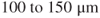 difference is insignificant to most users.
 - The performance of embedded and discrete touch is roughly the same. Some display-makers are still climbing the learning curve but, in the long term, the performance is expected to be equal.
- The weight of embedded and discrete touch is the same, since they both use three pieces of glass (the two sheets of glass that make up the display, plus the required cover-glass).
- The power consumption of embedded and discrete touch is roughly the same. Over time, the higher level of integration that is possible with embedded touch should allow it to consume less power.
- The cost of embedded touch and discrete touch are surprisingly close. It is currently possible to save $2 to $4 in controller and flex-cable cost in a smartphone due to the higher level of integration possible with embedded touch. As embedded touch expands into tablet-size displays, discrete touch could actually become lower in cost due to the replacement of ITO with other materials such as metal mesh.
- Off-screen touch icons (such as the Menu icon in an Android smartphone) can easily be created with discrete touch, since the cover-glass is always larger than the active area of the display. Embedded touch, on the other hand, must use additional components (e.g., capacitive buttons) to provide off-screen touch-icons.
Embedded touch has been under development for at least 10 years. All of the original development was focused on inventing new methods of detecting touch that were an integral part of, and leveraged the design of, the LCD [63]. The main methods included the following:
- “Pressed capacitive” (also called “charge-sensing”, first mass-produced by Samsung), where pressure on the display caused a change in the dielectric constant of the liquid crystal. The change in dielectric constant changed the capacitance between a pair of electrodes added into some or all pixels [64] [65].
- “Light-sensing”, first mass-produced by Sharp, where IR photo-detectors were added into some or all pixels. The photo-detectors read either the shadow of the touch-object in bright ambient light or the reflected backlight from the touch-object in dim ambient light or darkness [66].
- “Voltage sensing” (also called “digital switching”, first produced by Samsung), where micro-switches for X and Y location were added into some or all pixels. Pressure on the display closed the micro-switches, identifying the location of the press [67].
None of these methods were fully successful, although Samsung did ship several million units in a series of point-and-shoot digital cameras using pressed capacitive. The main reasons these methods were not successful were:
- insufficient signal-to-noise ratio for robust operation;
- the requirement to actually deflect the display surface (which eliminated the possibility of using a cover glass, thus increasing the probability of display damage); and
- the unreliability of pressing the display very close to the frame, where the color-filter glass has little ability to move.
Once the mutual-capacitive form of p-cap became widely adopted as the technology of choice for discrete touch in smartphones, the display industry realized that figuring out how to integrate p-cap into a display was the right way to go rather than trying to invent something entirely new. Table 2.16summarizes the three methods that have been developed for integrating p-cap into displays as embedded touch.
Table 2.16 Definitions of on-cell, in-cell, and hybrid embedded touch-technology along with the first company to ship a high-volume consumer product in each category
| Method | Definition | First Shipment |
| On-cell | Touch sensor is an array of ITO electrodes on the top surface of an LCD's color filter glass or an OLED's encapsulation glass; functionality is the same as standard p-cap | Samsung, in 2010 OLED smartphone |
| Hybrid in-cell/on-cell | Touch sensor is an array of ITO electrodes with the sense electrodes on top of the color filter (outside the cell) and the drive electrodes inside the LCD cell. The drive electrodes can be on the TFT glass (in IPS (in-plane switching) LCDs) or on the underside of the color-filter glass (in non-IPS LCDs). | Sony, in 2012 Sony and HTC smartphones |
| In-cell | Touch sensor is physically inside the LCD cell (between the TFT glass and the color-filter glass). Touch sensor can be either an array of ITO electrodes (mutual capacitive) or light-sensing elements | Apple, in 2012 iPhone-5 (capacitive); Sharp, in 2009 netbook (light-sensing) |
From a shipment perspective, in February 2010 Samsung was the first to ship on-cell embedded touch in a high-volume consumer product, the S8500 Super AMOLED™ smartphone (“Super AMOLED” is actually Samsung's brand name for their active-matrix OLED display enhanced with on-cell embedded touch). In May 2012, Sony was the first to ship hybrid in-cell/on-cell embedded touch in the Sony Xperia ![]() and the HTC EVO Design
and the HTC EVO Design ![]() smartphones; Synaptics developed the touch controller for these products [68]. In September 2012, Apple was the first to ship in-cell embedded touch in the iPhone-5. From an invention (patent) perspective, it remains to be seen if one company (e.g., Apple) will be credited with inventing all forms of capacitive embedded touch, or if each type of capacitive embedded touch will be credited separately.
smartphones; Synaptics developed the touch controller for these products [68]. In September 2012, Apple was the first to ship in-cell embedded touch in the iPhone-5. From an invention (patent) perspective, it remains to be seen if one company (e.g., Apple) will be credited with inventing all forms of capacitive embedded touch, or if each type of capacitive embedded touch will be credited separately.
In 2013, embedded touch is found mainly in smartphone (small) displays, the reason being that scaling embedded touch to larger displays is still under development. It is expected that, by 2015, the technology will have scaled to notebook-sized (15-inch) displays. The primary problems in scaling up embedded touch are as follows:
- Larger screens have more electrodes, since the number of sense and drive electrodes is a function of the physical dimensions of the screen, not the pixel-resolution of the screen. The electrodes are also longer. Both of these factors increase the amount of time required to complete a scan of the complete touchscreen.
- Larger screens often have higher pixel-resolution, which shortens the amount of time during which the display is electrically quiet. Embedded touch-sensing is typically done during these quiet periods (in fact, the touch controller and the display controller are usually synchronized in order to optimize this timing).
The combination of these two problems – more time required per scan, and less time in which to do it – has so far prevented scaling embedded touch beyond about seven inches in mass production, and 12 inches in the lab.
2.8.1 On-cell Mutual-capacitive (#14)
On-cell mutual capacitive is conceptually the simplest form of embedded touch. Instead of being constructed on a separate sheet of glass or on the underside of the cover-glass, a p-cap touchscreen is constructed on top of an LCD's color filter glass or an OLED's encapsulation glass (see Figure 2.11 in the P-Cap Touch Sensors section). The layer stack-ups and the resulting functionality are essentially identical to those of discrete p-cap. The most common electrode pattern used in on-cell is the interlocking diamond, because it can be manufactured in one layer with bridges.
As noted above, the first mass-production of on-cell embedded touch was in an OLED smartphone. Producing on-cell touch is actually easier (and higher yield) on an OLED display than on an LCD because the OLED encapsulation glass does not have anything on the underside. The underside of the color-filter glass in an LCD has at least the color filter material on it; if it is a non-IPS LCD, it also has the common voltage (Vcom) electrodes (made of ITO) on it. For a display manufacturer, the question then becomes which side to manufacture first. If the touchscreen side is made first, it can be annealed at a high temperature, which improves the quality of the ITO and, thus, the performance of the touchscreen, but the glass cannot be thinned as usual after sealing the LCD cell, which makes the display about 0.3 mm thicker. If the color-filter side is made first, then the glass can be thinned, but the touchscreen cannot be annealed at high temperature (doing so would damage the color-filter material), and this results in a lower-performing touchscreen [69]. Typically display-makers choose the latter because: (a) it does not interfere with the yield of the LCD production process; and (b) thinness is always seen as extremely important.
2.8.2 Hybrid In-cell/On-cell Mutual-capacitive (#15)
As the name implies, hybrid in-cell/on-cell embedded touch is half inside and half outside the LCD. The sense electrodes are deposited on top of the LCD's color-filter glass (outside the cell). Some IPS displays have a grounded anti-static shield layer made of a uniform layer of ITO on top of the color filter; if this is present, that layer is patterned into strips. It still works as a shield because all of the strips except the one being sensed at any given moment are grounded. This method of anti-static shielding is in the process of being replaced by the presence of a conductive layer in the display's top polarizer. In this situation, the sense electrodes are added as an entirely new layer on top of the color-filter glass.
The drive electrodes are created by grouping and repurposing the LCD's Vcom electrodes to act as part of a touch-sensing system in addition to their normal display-updating function [70]. In an IPS display, these electrodes are located on the TFT glass. In a non-IPS display, these electrodes are located on the underside of the cover-filter glass. Since these two surfaces are only a few microns apart, there is no different in performance between the two arrangements. The number of Vcom electrodes that are grouped together to form a single embedded p-cap drive electrode depends on the pixel resolution, the physical size of the screen, and the desired electrode spacing.
For example, a 7-inch, ![]() LCD has an active area of
LCD has an active area of ![]() . If embedded p-cap drive electrodes are to be formed horizontally along the long side of the display, and an electrode pitch of around 4.8 mm is desired, then dividing the 1280 pixels into 32 groups produces p-cap drive electrodes made up of 40 grouped Vcom electrodes, at a pitch of slightly more than 4.8 mm. The sense electrodes (on top of the color-filter glass, as explained above) would run vertically along the short side of the display, yielding 18 sense electrodes at the same pitch. Figure 2.34 illustrates a hybrid in-cell/on-cell structure, using Japan Display's (formerly Sony) “Pixel Eyes” [71] as an example. The figure shows both the physical arrangement of the electrodes, as well as the stack-up (not to scale).
. If embedded p-cap drive electrodes are to be formed horizontally along the long side of the display, and an electrode pitch of around 4.8 mm is desired, then dividing the 1280 pixels into 32 groups produces p-cap drive electrodes made up of 40 grouped Vcom electrodes, at a pitch of slightly more than 4.8 mm. The sense electrodes (on top of the color-filter glass, as explained above) would run vertically along the short side of the display, yielding 18 sense electrodes at the same pitch. Figure 2.34 illustrates a hybrid in-cell/on-cell structure, using Japan Display's (formerly Sony) “Pixel Eyes” [71] as an example. The figure shows both the physical arrangement of the electrodes, as well as the stack-up (not to scale).
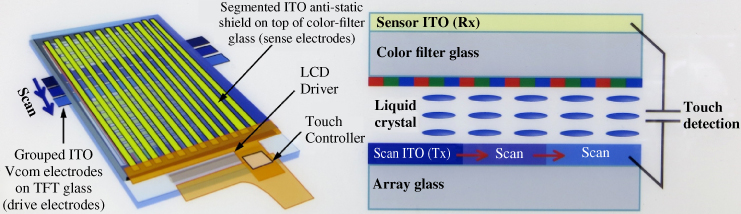
Figure 2.34 Japan Display's “Pixel Eyes” hybrid in-cell/on-cell touchscreen structure. The right side of the drawing shows that the drive electrodes are integrated into the TFT layer, while the sense electrodes are placed on top of the color-filter glass. The left side of the drawing provides more physical detail, showing that the sense electrodes are formed by segmenting the ITO anti-static shield, while the drive electrodes are formed by grouping Vcom electrodes. Also shown is an FPC containing the display and touch controllers, and connecting to both sets of electrodes.
Source: Japan Display, with annotation by the author.
The method described above is actually only one of several different ways that hybrid in-cell/on-cell can be implemented. Another method, described in patents by Apple and Samsung, is to use metal overlaid on the black matrix (on the underside of the color-filter glass) as drive electrodes, instead of repurposing anything on the TFT glass.
With on-cell embedded touch, it is quite possible to use a standard touch controller ASIC that has no connection to the LCD – after all, the touch electrodes in on-cell are only slightly closer to the LCD than they are in direct-bonded OGS, so increased LCD noise is not a big problem. But once part of the touch system moves inside the LCD, synchronization between the touch system and the LCD becomes necessary in order to deal with LCD noise.
2.8.3 In-cell Mutual-capacitive (#16)
As the name implies, in-cell embedded touch is located entirely inside the LCD cell. As noted previously, Apple was the first to ship high-volume in-cell embedded touch in the iPhone-5 smartphone in September 2012. The configuration used by Apple in the iPhone-5 is to put both the drive and sense electrodes on the TFT glass of an IPS LCD. This is accomplished using the same basic technique of grouping and repurposing the Vcom electrodes as described in the Hybrid In-Cell/On-Cell section above, except that the Vcom electrodes are grouped into two separate sets – one for drive and one for sense. In reality, this is much more difficult than it sounds.
Figure 2.35 illustrates how the grouping is done. This figure, created by BOE Technology Group's Central Research Institute, attempts to translate the drawings in Apple's patents [72] into a more easily-understandable form [73] (note, however, that the perspective is not quite right; each square is actually 54 pixels high by 126 pixels wide, so they should be drawn as rectangles). As shown in the key to the figure, the rows labeled “TX” are groups of horizontal (X) segmented Vcom electrodes, made of ITO and connected together by gate metal (in black). Each row is connected to the touch controller by touch-panel metal (labeled “TP” in the key). Since the display in the figure is 1,080 pixels high and there are 20 drive electrodes (rows), each group contains 54 Vcom electrodes. The wider columns are vertical (Y) Vcom electrodes connected via touch sense-detection metal (labeled “S/D” in the key); each of the ten columns also contains 54 Vcom electrodes. From a touchscreen perspective, the drive and sense electrodes are symmetrical. The narrow columns on each side of the wider ones are electrically connected but isolated dummy ITO (dummy ITO is often used in touch electrodes to achieve a more uniform visual appearance).
Figure 2.35 A schematic representation of how the Vcom electrodes in the TFT array of the iPhone-5 are grouped to produce both drive and sense electrodes.
Source: Adapted from BOE Technology Group's Central Research Institute.
It is important to understand that the particular technique used by Apple in the iPhone-5 is only one of several different ways that in-cell embedded touch can be implemented. For example, patents by Apple and Samsung describe a method where the drive electrodes are made by segmenting Vcom, but the sense electrodes are made of metal overlaid on the black matrix (on the underside of the color filter glass). The same two companies describe in their patents another method where the sense electrodes are metal on the black matrix (as just described) and the drive electrodes are ITO stripes deposited on top of a dielectric layer over the color filter material. Sharp described, at a display conference in 2012, a method where both touch electrodes are deposited on the bare underside of the color-filter glass, before the black matrix and color-filter material are applied. LG Displays described in one of their patents an unusual self-capacitive method using just the segmented Vcom electrode.
There are two methods of synchronizing the touch controller with the display controller (TCON): (1) modifying both controllers slightly and connecting them via several lines; or (2) combining the two controllers into a single chip. Synaptics was the first touch-controller company to do both of these. The primary advantage of the second method is that it reduces the touch-system bill of materials (BOM) cost by a dollar or two, while adding some NRE (non-recurring engineering) cost for the chip development; the primary disadvantage is that the combined controller becomes unique to a particular display resolution and pixel configuration. Clearly, the second method is only practical for very high-volume products (at least several million units).
The advantages and disadvantages of capacitive embedded touch-technology are shown in Table 2.17 below.
Table 2.17 Advantages and disadvantages of capacitive embedded touch-technology
| Embedded capacitive advantages | Embedded capacitive disadvantages |
| Most of the advantages of p-cap (robust multi-touch, if properly implemented in the controller algorithms; extremely light touch; allows bezel-less cover-glass; excellent optical performance; sealable; etc.) | In-cell and hybrid are practical only for very high-volume displays (millions of units); on-cell can be produced in lower quantities, but it may reduce yield of LCD manufacturing |
| Requires less “parameter tuning” than discrete capacitive for each new implementation in a product | Currently cannot be scaled above 12 inches; may never be as scalable as discrete |
| Lower cost than discrete capacitive (OGS), but not radically lower and definitely not “free”; difference may decrease when OGS starts to use ITO-replacement materials | More difficult to achieve same touch performance as discrete; display-maker may prioritize display yield over touch performance |
| Slightly thinner than discrete (typically 100–150 µm) | Controller manufacturers may be slower to migrate p-cap enhancements (e.g., water resistance, active stylus, etc.) to embedded versions |
| Power consumption may be slightly lower than discrete, especially with integrated touch and display controller | Display-maker may not be willing to produce same cover-glass variety and features as discrete touch-panel maker, or be as willing to do direct-bonding |
| Opportunity for touch-latency reduction, especially with integrated touch and display controller | Cannot support off-screen icons without additional components (unlike discrete) |
| May not be able to work through extremely thick glass | |
| No absolute pressure-sensing; only relative finger-contact area (same as p-cap) |
2.8.4 In-cell Light Sensing (#17)
In-cell light-sensing embedded touch is accomplished by adding a photo-detector into some or all pixels of an LCD (see Figure 2.36). As previously noted in Table 2.16, Sharp was the first to mass-produce a consumer product incorporating in-cell light-sensing in May 2009; the product was a netbook with a display-based touchpad. The display was a 4-inch LCD that used Sharp's CG (continuous grain) silicon technology with ![]() pixels (245 ppi). Originally Sharp wanted to use one sensor per pixel, in order to enable the display to be also used as a scanner, but they found that doing so reduced the display aperture-ratio too much. Instead, they used one sensor per nine pixels, which produced a scanning resolution of only 27 ppi – not high enough for practical use. Even at one sensor per nine pixels, Sharp found that processing the output of the light-sensors required more CPU bandwidth than their touch controller could provide, so the performance of the display-based touchpad turned out to be very poor (only 25% of the speed of a typical capacitive touchpad).
pixels (245 ppi). Originally Sharp wanted to use one sensor per pixel, in order to enable the display to be also used as a scanner, but they found that doing so reduced the display aperture-ratio too much. Instead, they used one sensor per nine pixels, which produced a scanning resolution of only 27 ppi – not high enough for practical use. Even at one sensor per nine pixels, Sharp found that processing the output of the light-sensors required more CPU bandwidth than their touch controller could provide, so the performance of the display-based touchpad turned out to be very poor (only 25% of the speed of a typical capacitive touchpad).
Figure 2.36 Conceptual diagram of in-cell light-sensing embedded touch. The light-sensor is an aSi photo-transistor; it is placed in the blue (lowest) sub-pixel because the sensor's peak response is in the blue-green spectral range. The drawing in the right side of the figure shows IR light emitted from an IR-LED in the backlight being reflected from a touching finger and seen by the light-sensor.
Source: Adapted from [4] (left) and Samsung (right).
Research in this area in the first half of the 2000s used visible-light sensors, with the expectation that the sensor would see the shadow of the touch-object in bright ambient light or the reflection of the backlight from the touch-object in dim ambient light [74] [75]. Once researchers realized, around 2006, that visible light was too restrictive (among other things, it cannot get through a black image on the LCD), the researchers switched to IR light sensors. This change also meant that IR emitters needed to be added to the backlight. Because LCDs are only moderately transparent to IR light, and the light is attenuated on both trips through the LCD, the IR emitters are required to have relative high-intensity emission. The additional power consumed by the IR LEDs in Sharp's display significantly reduced the netbook's battery life.
Between Sharp's netbook in 2009 and today (2013), there have been only two commercial products that use light-sensing embedded touch. The first is a 21-inch consumer monitor developed by IDTI (Integrated Digital Technologies, Inc.) in Taiwan [76]. Initially designed for use only with a light-pen, later versions were enhanced to support finger touch using the visible light shadow/reflection method mentioned in the previous paragraph.
The second product is the Samsung SUR40 40-inch all-in-one table computer created jointly with Microsoft for use in Microsoft Surface 2.0 [77]. This LCD includes IR emitters in the backlight, and uses one IR photo-sensor per eight pixels. In an attempt to improve the sensitivity of the touch system, Samsung used aSiGe (amorphous silicon-germanium) light sensors, which are about 15 times more sensitive than ordinary silicon light-sensors. While this definitely improved the touch sensitivity, it introduced a new problem: extreme sensitivity to ambient IR. The problem is so extreme that Samsung published a manual documenting the maximum lux that the touch system can tolerate in each type of room lighting; the number for incandescent light is only 50 lux [60]. The product includes a utility program that measures the ambient IR illumination and displays red-yellow-green areas on the screen to indicate whether the illumination level is low enough.
Samsung is currently researching the use of in-stack light-sensing embedded touch for OLED displays [78]. The concept is parallel to that described for LCDs: IR-emitting pixels in the OLED stack, with IR-detecting sensors in the active-matrix backplane.
Although research and development on in-cell light-sensing embedded touch has been going on for more than 10 years, it is still an emerging technology with unsolved challenges and no successful high-volume consumer products. Table 2.18 provides a more detailed look at the advantages and disadvantages of in-cell light-sensing embedded touch.
Table 2.18 Advantages and disadvantages of in-cell light-sensing embedded touch technology
| In-cell light-sensing advantages | In-cell light-sensing disadvantages |
| Some of the advantages of embedded capacitive (extremely light touch; allows bezel-less cover-glass; sealable; etc.) | Practical only for high-volume displays because fundamentally it's a unique display design |
| May be lowest-cost form of embedded touch (only one set of sensors; easier to integrate into LCD structure with less material), although image-processing requirements may offset some of that | More difficult to achieve same touch performance as discrete or embedded capacitive; processing sensor output data requires using CPU/GPU-intensive image-processing software (same as vision-based touch) |
| No formal size limit (40 inches is the largest as of 2013) | Reduced optical performance (lower LCD aperture ratio due to light sensors; lower OLED light output due to IR emitters) |
| Slightly thinner than discrete capacitive (typically 100 to |
Sensitive to ambient IR; worse if more sensitive photo-detectors are used; difficult to avoid saturating photo-sensors in very bright ambient IR |
| Requires much less “parameter tuning” than either discrete or embedded capacitive touch-sensing | Low signal-to-noise ratio (poor touch sensitivity) at the crossover point where the IR reflected from the touch-object is equal to the ambient IR |
| Less sensitive to external RFI/EMI | Low signal levels from photo-sensors make touch-sensing more sensitive to internal interference (e.g., stray current from adjacent photo-sensor) |
| Reduced touch sensitivity as the touch surface moves further away from the LCD (i.e., air-gap, thicker cover-glass required for larger displays, etc.) | |
| Optical-sensor density (ppi) is not high enough to enable using the display as a scanner | |
| Increased power consumption due to IR emitters | |
| Cannot support off-screen icons without additional components (same as embedded capacitive) |
2.9 Other Touch Technologies
2.9.1 Force-sensing (#18)
Force-sensing has always been seen as the “holy grail” of touch-sensing, because the simplest possible method of detecting a touch should be to just measure the pressure (force) of the touch in multiple locations on the substrate and then triangulate to find the origin. If only it were that simple!
The earliest known commercial product based on force-sensing was IBM's “TouchSelect” touch overlays for 12″ to 19″ CRT monitors in 1991. This technology used strain gauges to mount the touchscreen. It was unsuccessful, lasting no more than about three years on the market. The next commercial incarnation of force-sensing touch in the USA was launched in 2007 by QSI, a Utah-based manufacturer of human-machine interface products and mobile data terminals. The technology, branded as ![]() , employed a clever beam-mounting method for the strain gauges that eliminated any horizontal component of the touching force [79]. In order to avoid impacting their existing business, QSI spun off the force-sensing technology in 2008 into a subsidiary named Vissumo [80]. The subsidiary was insufficiently capitalized to undertake the non-trivial task of selling a new touch-technology into a crowded market, so they ran out of money and shut down in 2009 (QSI was acquired by Beijer Electronics in 2010 and is now known under that name).
, employed a clever beam-mounting method for the strain gauges that eliminated any horizontal component of the touching force [79]. In order to avoid impacting their existing business, QSI spun off the force-sensing technology in 2008 into a subsidiary named Vissumo [80]. The subsidiary was insufficiently capitalized to undertake the non-trivial task of selling a new touch-technology into a crowded market, so they ran out of money and shut down in 2009 (QSI was acquired by Beijer Electronics in 2010 and is now known under that name).
In a separate attempt at commercializing force-sensing touch, MyOrigo in Finland in 2000 developed a force-sensing touchscreen for an advanced user-interface on a proposed smartphone. MyOrigo was sold to its management in 2004 and restarted as F-Origin. F-Origin went bankrupt in Finland in 2005 and the assets were purchased by a US investor who re-formed F-Origin in the US in 2006. F-Origin further developed its force-sensing technology (branded as ![]() ) during 2007–2008, but could not get any traction in the consumer electronics market, due to the rapidly growing prevalence of p-cap. They restructured in 2009 with an ownership investment from TPK (the world's largest supplier of p-cap), and began marketing zTouch in 2010. F-Origin is currently focused on commercial applications, where the durability and environmental resistance of force-sensing touch technology are particularly valuable [81].
) during 2007–2008, but could not get any traction in the consumer electronics market, due to the rapidly growing prevalence of p-cap. They restructured in 2009 with an ownership investment from TPK (the world's largest supplier of p-cap), and began marketing zTouch in 2010. F-Origin is currently focused on commercial applications, where the durability and environmental resistance of force-sensing touch technology are particularly valuable [81].
Force-sensing touch works by supporting the display (or cover-glass) on force sensors, typically either strain gauges or piezoelectric transducers. In order to obtain accurate measurements of the force applied to the touch surface, the display and/or cover-glass's movement must be constrained so that it only moves in the Z-direction. There are several ways of accomplishing this. Figure 2.37 illustrates the suspension spring-arm method currently employed by F-Origin.
Figure 2.37 In F-Origin's force-sensing touch technology, the LCD/cover-glass/front-bezel assembly is supported by two suspension spring-arms whose middle is anchored to the device housing (product chassis) and whose ends are attached to the assembly. Four piezo-electric pressure sensors are located at the corners of the assembly, placed between the assembly and the device housing. Since the assembly can only move in the z-direction due to the constraint provided by the suspension spring-arms, any pressure on the assembly (e.g., on the display cover-glass) can be detected and localized by the four piezo-electric sensors.
Source: Adapted from F-Origin, with additional annotation by the author.
The advantages and disadvantages of force-sensing touch-technology are shown in Table 2.19 below. Note that this analysis does not include new force-sensing methods that have not emerged yet, such as that from NextInput, which uses an array of force-sensing organic transistors under the display [82].
Table 2.19 Advantages and disadvantages of force-sensing touch technology
| Force-sensing advantages | Force-sensing disadvantages |
| High optical performance due to plain-glass substrate | Difficult to achieve multi-touch (two touches requires eight sensors; the number of sensors increases exponentially after that) |
| Touch-surface independence (substrate can be any rigid material); can use 3D substrates with embedded moving objects (this is unique) | Minimum touch-force required is close to zero but not actually zero, like p-cap |
| Activation by any object with close to zero touch-force (stylus independence); even better than resistive | Difficult but not impossible to achieve flush (bezel-less) screen design |
| Pressure-sensitive; pressure can replace hover (press lightly to display choices; press harder to select); pressure can also can be used to minimize false touches | Cannot meet Win8 touch specifications due to lack of five-touch multi-touch; this limits it to commercial or non-Windows consumer applications |
| Inherently durable; can easily be designed to handle extended environmental conditions | Mechanical nature of touch-sensing mechanism reduces reliability |
| Relatively low cost due to sensor simplicity (substrate plus four piezoelectric sensors) | Most sensors add volume to the system (thickness or footprint) |
| No pre-touch (user must actually touch the substrate to register a touch) | |
| Insensitive to EMI/RFI and ambient light | |
| Continuous calibration filters out environmental conditions such as vibration | |
| Has been scaled up to 42 inches; theoretically can go higher |
Earlier in this chapter, a prediction was made that multi-touch will eventually become significant in commercial applications. Given that prediction, force-sensing technology seems likely to disappear in the next five years, or at best be relegated to a very small niche.
2.9.2 Combinations of Touch Technologies
It should be clear from the information presented in this chapter that “there is no perfect touch technology”. No single technology meets all the requirements of all applications. Combinations of technologies are one approach to creating a better touchscreen. Examples can be found in Tablet PCs, e-readers, and point-of-sale terminals. An example of each follows.
The latest Microsoft Tablet PCs often combine a p-cap finger-capable touchscreen with an electromagnetic (EM) pen-digitizer. The dominant vendor of EM pen-digitizers (Wacom in Japan) offers a single controller that can drive both the touchscreen and the pen-digitizer, which enables automatic mode-switching between finger and pen [83].
In May 2011, Hanvon announced a new method of combining technologies to accomplish the same goal of pen-and-finger operation. Hanvon combines their EM pen-digitizer with an array of pressure-sensing piezo-capacitors in the same plane as the EM sensor under the display. The piezo-capacitors, which are the same component that is used in the tip of the pen for pressure-sensing, enable sensing finger pressure through (rather than on top of) an e-reader's electronic paper display (EPD).
One of the major providers of POS terminals prefers to use traditional IR in their products. However, to minimize the problem of “pre-touch” (where the finger breaks the IR light beams and triggers a touch without actually touching the surface of the display), the provider includes a pressure-sensing piezoelectric transducer in the touchscreen mounting scheme so that touch coordinates are produced only when the user is guaranteed to be touching the screen. In this application, the transducer detects the presence of a touch, while the traditional IR touchscreen detects the location of the touch.
Combinations of touch technologies are very likely to continue to exist during the next five years, although combinations of major technologies are usually limited by the cost of the combination. Combinations of a major and minor technology are more likely to occur, as in the example above of combining traditional IR with a pressure sensor. Combinations of current touch technologies with emerging human-machine interface (HMI) technologies are also likely to occur; for example, p-cap combined with a low-cost, miniature 3D camera to enable the detection of near-field gestures in the space above the touchscreen, beyond the range of hover detection. Ultimately, it should be possible to manipulate an object on the p-cap touchscreen and then “pull” the object out of the 2D screen into the 3D space between the screen and the user, seamlessly transitioning the object manipulation from the p-cap touchscreen to the 3D camera.
2.10 Summary
This chapter has described 18 current touch technologies (plus several obsolete technologies) in a fair amount of detail. The best way of summarizing such an ungainly body of information is by predicting how the 18 touch technologies are likely to evolve in the next five to ten years, as shown in Table 2.20below:
Table 2.20 This table presents predictions of how the 18 touch technologies described in this chapter are likely to evolve in the next five to ten years
| # | Touch technology | Predicted outcome |
| 1 | Projected Capacitive | Remains #1 in consumer devices; significant growth in commercial applications |
| 2 | Surface Capacitive | Disappears from the market in 5–7 years |
| 3 | Analog Resistive | Major reduction, but never completely disappears from the market |
| 4 | Digital Multi-Touch Resistive | Niche commercial and military applications |
| 5 | Analog Multi-Touch Resistive | Niche commercial and military applications |
| 6 | Surface Acoustic Wave (SAW) | Moderate continued growth in commercial applications |
| 7 | Acoustic Pulse Recognition (APR) | Niche non-display applications (touch-sensitive surfaces and devices) |
| 8 | Dispersive Signal Technology (DST) | Disappears from the market in less than five years |
| 9 | Traditional Infrared | Moderate reduction in large format; significant reduction in commercial applications; potential growth in mobile devices with reflective displays |
| 10 | Multi-Touch Infrared | Limited growth until multi-user gaming and/or collaboration applications become common and the cost of the technology drops to consumer levels |
| 11 | Camera-Based Optical | Significant growth only over 40″ |
| 12 | In-Glass Optical (PSD) | Niche applications in large format, with potential applications in consumer all-in-one desktop computers |
| 13 | Vision-Based | Niche applications in large format |
| 14 | Embedded On-Cell Capacitive | Significant growth only in high-volume consumer devices; will become the most popular form of embedded touch due to minimum interference with the LCD cell process |
| 15 | Embedded Hybrid Capacitive | Significant growth only in high-volume consumer devices; #2 in popularity |
| 16 | Embedded In-Cell Capacitive | Significant growth only in high-volume consumer devices; #3 in popularity due to the high level of modification required in the LCD cell process |
| 17 | Embedded In-cell Light-Sensing | Disappears from the market in less than five years unless there's a breakthrough in solving the current problems |
| 18 | Force Sensing | Disappears from the market in less than five years or becomes a very small commercial niche |
2.11 Appendix
All touch-technology suppliers mentioned in this chapter (excluding ones no longer in business) are listed in alphabetical order in Table 2.21, along with the technologies they supply and their website URL.
Table 2.21 This table lists all the touch technology suppliers mentioned in this chapter (excluding ones no longer in business), along with the technologies they supply, and their website URL
| Company | Technologies | URL |
| 3M Touch Systems | 1,2,8 | www.3mtouch.com |
| Apex Material Technology (AMT) | 1,3,5 | www.amtouch.com.tw |
| Apple | 1,15 | www.apple.com |
| Atmel | 1 | www.atmel.com |
| Baanto | 11 | www.baanto.com |
| Citron | 10 | www.citron.de |
| Cypress Semiconductor | 1 | www.cypress.com |
| Elo Touch Solutions | 1,2,3,6,7,9 | www.elotouch.com |
| FlatFrog | 12 | www.flatfrog.com |
| F-Origin | 18 | www.f-origin.com |
| General Touch | 1,3,6,9,10,11 | www.generaltouch.com |
| Gunze USA | 1,3,4 | www.gunzeusa.com |
| IDS Pulse | 10 | www.idspulse.com |
| Integrated Digital Technologies (IDTI) | 17 | www.idti.com.tw |
| Japan Display (JDI) | 16 | www.j-display.com |
| JTouch | 1,3,5 | www.jtouch.com.tw |
| LG Displays | 1,15 | www.lgdisplay.com |
| Lumio | 1,6,10,11 | www.lumio.com |
| Microsoft | 13 | www.microsoft.com |
| MultiTouch | 13 | www.multitaction.com |
| Nissha | 1,3 | www.nissha.com |
| Peratech | 4 | www.peratech.com |
| Planar | 1,3,6,10,11 | www.planar.com |
| PQ Labs | 10 | www.pqlabs.com |
| Quanta | 11 | www.quantatw.com |
| Samsung | 14,15,17 | www.samsung.com |
| Sharp | 15,17 | www.sharp-world.com |
| Shenzhen TimeLink Technology | 10 | www.timelink.cn |
| SMART Technologies | 11 | www.smarttech.com |
| Stantum | 4 | www.stantum.com |
| Synaptics | 1,16 | www.synaptics.com |
| Texas Instruments | 1,3,5 | www.ti.com |
| TPK | 1 | www.tpk.com |
| Visual Planet | 1 | www.visualplanet.biz |
| Wacom | 1,2 | www.wacom-components.com |
| ZaagTech | 10 | www.zaagtech.com |
| Zytronic | 1 | www.zytronic.co.uk |
References
- 1. Johnson, E.A. (1965). Touch Display – A Novel Input/Output Device for Computers. Electronics Letters 1(8), 219–220.
- Further Reading:
- Johnson, E.A. (1967). Touch Displays: A Programmed Man-Machine Interface. Ergonomics 10(2), 271–277.
- Orr, N.W., Hopkins, V.D. (1968). The Role of Touch Display in Air Traffic Control. The Controller 7, 7–9.
- 2. Shneiderman, B. (1991). Touch screens now offer compelling uses. IEEE Software 2,93–94, 107.
- 3. Walker, G. (2007). Touch and the Apple iPhone, Veritas et Visus Touch Panel 12, 50–54, (http://www.walkermobile.com/Touch_And_The_Apple_iPhone.pdf, retrieved 10/15/13).
- 4. DisplaySearch, 2008–2013. Touch-Panel Market-Analysis Annual Reports.
- 5. Buxton, B. (2007–2013). Multi-Touch Systems that I Have Known and Loved. Microsoft (www.billbuxton.com/multitouchOverview.html, retrieved 9/25/13).
- 6. Wigdor, D. (2011). The Breadth-Depth Dichotomy: Opportunities and Crises in Expanding Sensing Capabilities. Information Display 3, 18–23, (http://informationdisplay.org/IDArchive/2011/March/EnablingTechnologyTheBreadthDepthDichotomy.aspx, retrieved 10/15/13).
- Further Reading:
- Wigdor, D., Wixon, D. (2011). Brave NUI World: Designing Natural User Interfaces for Touch and Gesture. Morgan Kaufmann (Elsevier), Burlington, MA.
- 7. Stumpe, B. (1977). A New Principle for X-Y Touch System, CERN (http://cds.cern.ch/record/1266588/files/StumpeMar77.pdf, retrieved 10/15/13).
- Further Reading:
- Stumpe, B., Sutton, C. (2010). The First Capacitive Touch Screens at CERN. CERN Courier (http://cerncourier.com/cws/article/cern/42092, retrieved 10/15/13).
- CERN Bulletin (2010). Another of CERN's Many Inventions. BUL-NA-2010-063, (http://cds.cern.ch/record/1248908, retrieved 10/15/13).
- Beck, F., Stumpe, B. (1973). Two Devices for Operator Interaction in the Central Control of the New CERN. CERN (http://cds.cern.ch/record/186242/files/CERN-73-06.pdf?version=1, retrieved 10/15/13).
- Stumpe, B. (1978). Experiments to Find a Manufacturing Process for an X-Y Touch Screen. CERN (http://cds.cern.ch/record/1266589/files/StumpeFeb78.pdf, retrieved 10/15/13).
- 8. Logan, J. (1991). The History of MicroTouch: 1982–1992, a Decade of Touch Input. Pamphlet published by the founder of MicroTouch Systems.
- 9. Binstead, R. (2009). A Brief History of Projected Capacitance Development by Binstead Designs (http://binsteaddesigns.com/history1.html, retrieved 10/15/13).
- 10. Barrett, G., Omote, R. (2010). Projected-Capacitive Touch Technology. Information Display 3, 16–21, (http://informationdisplay.org/IDArchive/2010/March/FrontlineTechnologyProjectedCapacitiveTouchT.aspx, retrieved 10/15/13).
- Further Reading:
- 3M Touch Systems (2011). Touch Technology Brief: Projected Capacitive Technology (http://solutions.3m.com/3MContentRetrievalAPI/BlobServlet?lmd=1332776667000&locale=en_US&assetType=MMM_Image&assetId=1319224170371&blobAttribute=ImageFile, retrieved 10/15/13).
- 11. Wang, T., Blankenship, T. (2011). Projected-Capacitive Touch Systems from the Controller Point of View. Information Display 3, 8–12, (http://informationdisplay.org/IDArchive/2011/March/FrontlineTechnologyProjectedCapacitiveTouchS.aspx, retrieved 10/15/13).
- Further Reading:
- Lawson, R. (2012). Challenges and Opportunities in Touch-Controller Semiconductors, HIS.
- SID-IHS Future of Touch and Interactivity Conference, Boston, MA.
- 12. DisplaySearch (2013). Touch-Panel Market-Analysis Annual Report.
- 13. Poor, A. (2012). How It Works: The Technology of Touch Screens. Computerworld (http://www.computerworld.com/s/article/9231961/How_it_works_The_technology_of_touch_screens?taxonomyId=12&pageNumber=1, retrieved 10/15/13).
- 14. Bauman, C. (2007). How to Select a Surface-Capacitive Touch-Screen Controller. Information Display 12:, 32–36 (http://informationdisplay.org/IDArchive/2007/December/HowtoSelectaSurfaceCapacitiveTouchScreenCo.aspx, retrieved 10/15/13).
- 15. Harrah's Entertainment (2006). Profile of the American Casino Gambler (http://www.org.id.tue.nl/ifip-tc14/documents/HARRAH'S-SurveyCasinoGambler-2006.pdf, retrieved 10/15/13).
- 16. Wacom (2013). RRFC™ Reversing Ramped-Field Capacitive Touch-Technology (http://www.wacom-components.com/english/technology/touch.html, retrieved 10/15/13).
- 17. Wikipedia (2013). Touchscreen (http://en.wikipedia.org/wiki/Touchscreen, retrieved 10/15/13).
- 18. Emerson, L.G. (2010). Samuel Hurst – the ‘Tom Edison’ of ORNL. OakRidger (http://www.oakridger.com/article/20101214/NEWS/312149981?tag=1, retrieved 10/15/13).
- 19. Elo Touch Solutions (2013). History of Elo (http://www.elotouch.com/AboutElo/History/default.asp, retrieved 10/15/13).
- 20. Westinghouse Electric (1970). Interface Device and Display System. US Patent 3,522,664 (http://www.freepatentsonline.com/3522664.html, retrieved 10/15/13).
- 21. Sierracin/Intrex (1979). TransTech product brochure.
- 22. Downs, R. (2005). Using Resistive Touch Screens for Human/Machine Interface. Texas Instruments Analog Applications Journal (SLYT209A).
- 23. Barrett, G. (2012). Decoding Touch Technology: An Insider's Guide to Choosing the Right Touch for your Display. Touch International, white paper (http://touchinternational.com/literature/choosing-touch-technology-whitepaper.html, retrieved 10/15/13).
- Further Reading:
- Barrett, G. (2006). Frit and the Better Touch Screen. Touch International, white paper (http://touchinternational.com/literature/whitepapers/FritandtheBetterTouchScreen.pdf, retrieved 10/15/13).
- 24. DMC Co (2011). Technologies of Touch Screens – Analog 8-Wire Resistive (http://www.dmccoltd.com/english/museum/touchscreens/technologies/8-wire.asp, retrieved 10/15/13).
- 25. Semtech (2011). SX8677/SX8678 Haptics-Enabled Multitouch 4/5-Wire Resistive Touchscreen Controller with Proximity Sensing. Datasheet (http://www.semtech.com/images/datasheet/sx8677_8.pdf, retrieved 10/15/13).
- 26. Elo Touch Solutions (2013). AccuTouch ZeroBezel Technology Specifications (http://www.elotouch.com/Technologies/AccuTouch/accutouch_zero-bezel_specifications.pdf, retrieved 10/15/13).
- 27. Fenn, J. (2013). Turned Around a Potential Loss to Revolutionize a Business. Professional Resume (http://www.corporatewarriors.com/john7820/fenn.doc, retrieved 10/15/13).
- 28. DMC Co (2011). Technologies of Touch Screens – Digital Matrix Resistive (http://www.dmccoltd.com/english/museum/touchscreens/technologies/Matrix.asp, retrieved 10/15/13).
- 29. Largillier, G. (2007). Developing the First Commercial Product that Uses Multi-Touch Technology. Information Display 12, 14–18 (http://informationdisplay.org/IDArchive/2007/December/DevelopingtheFirstCommercialProductthatUses.aspx, retrieved 10/15/13).
- 30. Stantum (2012). Stantum's Newest Digital Resistive Touch-Panel (http://www.leavcom.com/stantum_061012.php, retrieved 10/15/13).
- 31. Texas Instruments (2011). Analog Matrix Touchscreen Controller. Datasheet (http://www.mouser.com/ds/2/405/sbas536b-94322.pdf, retrieved 10/15/13).
- 32. Apex Material Technology (AMT) (2013). Multi-Finger (MF) Touch (http://www.amtouch.com.tw/products/advanced-resistive-touch-screen/multi-finger-mf-touch/, retrieved 10/15/13).
- 33. Adler, R., Desmares, P.J. (1985). An Economical Touch Panel Using SAW Absorption. IEEE Ultrasonics Symposium 1985, 499–502. (10.1109/ULTSYM.1985.198560).
- 34. Kent, J. et al. (2007). Robert Adler's Touchscreen Inventions. IEEE 2007 Ultrasonics Symposium, 9–20 (10.1109/ULTSYM.2007.18).
- 35. Elo Touch Solutions (1997–2001). Acoustic Touch Position Sensor Using a Low Acoustic Loss Transparent Substrate. US Patent 6,236,391 (http://www.freepatentsonline.com/6236391.html, retrieved 10/15/13).
- 36. Elo Touch Solutions (2010–2013). Acoustic Condition Sensor Employing a Plurality of Mutually Non-Orthogonal Waves. US Patent 8,421,776 (http://www.freepatentsonline.com/8421776.html, retrieved 10/15/13).
- 37. Microsoft (2013). Windows Certification Program: Hardware Certification Taxonomy & Requirements for Windows 8.1, Device Digitizer Requirements (http://msdn.microsoft.com/en-us/library/windows/hardware/jj134351.aspx, retrieved 10/15/13).
- 38. Elo Touch Solutions (2011–2013). Bezel-less Acoustic Touch Apparatus. US Patent 8,576,202 (http://www.freepatentsonline.com/8576202.html, retrieved 10/15/13).
- 39. North, K., D'Souza, H. (2006). Acoustic Pulse Recognition Enter Touch-Screen Market. Information Display 12, 22–25 (http://informationdisplay.org/IDArchive/2006/December/AcousticPulseRecognitionEntersTouchScreenMar.aspx).
- 40. Kent, J. (2010). New Touch Technology from Time Reversal Acoustics: A History. IEEE International Ultrasonics Symposium Proceedings 1173–1178.
- 41. Butcher, M. (2010). The $62 Million Sale of a Touch Tech Startup Adds to the Tablet Revolution. TechCrunch (http://techcrunch.com/2010/01/27/the-62-million-sale-of-a-touch-tech-startup-adds-to-the-tablet-revolution/, retrieved 10/15/13).
- 42. 3M Touch Systems (2008). Dispersive Signal Touch Technology: Technology Profile. White paper (http://multimedia.3m.com/mws/mediawebserver?mwsId=66666UF6EVsSyXTtmxTXoxfaEVtQEVs6EVs6EVs6E666666--&fn=DST%20Tech%20Profile.pdf, retrieved 10/15/13).
- 43. Wikipedia (2013). PLATO Computer System (http://en.wikipedia.org/wiki/PLATO_IV, retrieved 10/15/13).
- 44. Wikipedia (2013). HP-150 (http://en.wikipedia.org/wiki/HP_150, retrieved 10/15/13).
- 45. Elo Touch Solutions (2009). Elo TouchSystems IntelliTouch Plus Multi-Touch & Windows-7. Communication Brief (http://www.elotouch.com/pdfs/faq_ip.pdf, retrieved 10/15/13).
- 46. Charters, R. (2009). High-Volume Manufacturing of Photonic Components on Flexible Substrates. Information Display 12, 12–16 (http://informationdisplay.org/IDArchive/2009/December/FrontlineTechnologyHighVolumeManufacturingof.aspx, retrieved 10/15/13).
- 47. Thompson, M. (2009). RPO Digital Waveguide Touch. DisplaySearch 2009 Emerging Display Technologies Conference, San Jose, CA.
- Further Reading:
- Maxwell, I. (2007). An Overview of Optical-Touch Technologies. Information Display 10, 26–30 (http://informationdisplay.org/IDArchive/2007/December/AnOverviewofOpticalTouchTechnologies.aspx, retrieved 10/15/13).
- 48. Poa Sana (1997–1999). User Input Device for a Computer System. US Patent 5,914,709 (http://www.freepatentsonline.com/5914709.html, retrieved 10/15/13).
- 49. PQ Labs (2010–2012). System and Method for Providing Multi-Dimensional Touch Input Vector. US Patent Application 2012-0098753 (http://www.freepatentsonline.com/y2012/0098753.html, retrieved 10/15/13).
- 50. Zytronic (2013). Zytronic Reveals a New Dimension in Touchscreens for Gaming Machines. Press release (http://www.zytronic.co.uk/assets/Uploads/ZY370-G2E-2013-Zytronic-reveals-a-new-dimension-in-touchscreens-for-gaming-machines.pdf, retrieved 10/15/13).
- 51. PQ Labs website, (http://www.pqlabs.com, retrieved 10/15/13).
- 52. Walker, G. (2011). Camera-Based Optical Touch Technology. Information Display 3, 30–34 (http://informationdisplay.org/IDArchive/2011/March/FrontlineTechnologyCameraBasedOpticalTouchT.aspx), retrieved 10/15/13.
- 53. Baanto (2011). ShadowSense™ Touch Detection. White paper (http://baanto.com/uploads/Image/pdfs/whitepapers/shadowsense_touch_detection.pdf, retrieved 10/15/13).
- 54. Baanto (2011). Rain and Fluid Discrimination for Touchscreens. White paper (http://baanto.com/uploads/Image/pdfs/whitepapers/shadowsense_rain_rejection.pdf, retrieved 10/15/13).
- 55. Wassvik, O. (2013). PSD: In-Glass Optical Touch for Larger Form-Factors. DisplaySearch Emerging Display Technologies Conference, San Jose, CA.
- 56. Walker, G., Finn, M. (2010). Beneath the Surface. Information Display 3, 31–34, (http://informationdisplay.org/IDArchive/2010/March/EnablingTechnologyBeneaththeSurface.aspx).
- 57. Castle, A. (2009). Build Your Own Multitouch Surface Computer. Maximum PC (http://www.maximumpc.com/article/features/maximum_pc_builds_a_multitouch_surface_computer?page=0,0, retrieved 10/15/13).
- 58. NUI Group Authors (2009). Multitouch Technologies. e-book, NUI Group (http://www.google.com/url?sa=t&rct=j&q=&esrc=s&frm=1&source=web&cd=1&ved=0CCwQFjAA&url=http%3A%2F%2Fnuicode.com%2Fattachments%2Fdownload%2F115%2FMulti-Touch_Technologies_v1.01.pdf&ei=C7yBUqn6N4G3igKz9YDIDQ&usg=AFQjCNGWgAwHLy64d0YfObchamgKkeby8g&bvm=bv.56343320,d.cGE, retrieved 10/15/13).
- 59 Anttila, H. (2012). Multi-User Interactive Technology Advancements for Any Size Display. IHS Touch-Gesture-Motion Conference, Austin, TX.
- Further Reading:
- MultiTouch (2011). MultiTaction: Technology Platform for MultiTouch LCDs of Any Size. White paper http://multitouch.s3.amazonaws.com/resources/brochures_for_print/whitepaper_MultiTaction_v1-1_USletter_print.pdf, retrieved 10/15/13).
- 60. Samsung Electronics (2011). Samsung SUR40 for Microsoft Surface Venue Readiness Guide (http://www.samsung.com/us/pdf/sur40/SUR40_Venue_Readiness_Guide.pdf, retrieved 10/15/13).
- 61. Microsoft (2012). Tagged Object Integration for Surface 2.0. White paper. (http://download.microsoft.com/download/D/7/B/D7BE282A-FCB2-4A2C-AC48-6BC8441AB281/Tagged%20Objects%20for%20Surface%202.0%20Whitepaper.docx, retrieved 10/15/13).
- 62. Walker, G. (2013). Embedded Touch: The Touch-Panel Makers vs. The Display-Makers, FPD International Conference, Yokohama, Japan, (http://www.walkermobile.com/FPD_International_2013_Touch_Futures.pdf, retrieved 10/15/13).
- 63. Walker, G., Finn, M. (2010). LCD In-Cell Touch. Information Display 3, 8–14. (http://informationdisplay.org/IDArchive/2010/March/FrontlineTechnologyLCDInCellTouch.aspx, retrieved 10/15/13).
- 64. Lee, J. et al. (2007). Hybrid Touch Screen Panel Integrated in TFT-LCD. SID 2007 Symposium Digest 24.3.
- 65. Samsung Electronics (2004–2007). Liquid Crystal Display Device Having Touch Screen Function and Method of Fabricating the Same. US Patent 7,280,167 (http://www.freepatentsonline.com/7280167.html, retrieved 10/15/13).
- 66. Den Boer, W. et al. (2003). Active Matrix LCD with Integrated Optical Touch Screen. SID 2003 Symposium Digest 56.3.
- 67. Samsung Electronics (2007–2011). Touch Screen Display Apparatus and Method of Driving the Same. US Patent 8,072,430 (http://www.freepatentsonline.com/8072430.html, retrieved 10-15-13).
- 68. Ozbas, M. et al. (2012). An In-Cell Capable Capacitive Touchscreen Controller with High SNR and Integrated Display Driver IC for WVGA LTPS Displays. SID Symposium 2012 Digest 485–488.
- 69. Mackey, B. (2013). Touch + Display, Any Way You Want It, Synaptics. SID Display Week Conference (Session M8), Vancouver, Canada.
- 70. Synaptics. (2010). Capacitive Sensing Using a Segmented Common Voltage Electrode of a Display. US Patent Application 2010-0238134 (http://www.freepatentsonline.com/y2010/0238134.html, retrieved 10/15/13).
- 71. Noguchi, K. (2012). Trend of In-Cell Touch Panel Technologies. Sony, FPD International Conference, Yokohama, Japan.
- 72. Apple (2010). Integrated Touch Screen. US Patent 7,859,521 (http://www.freepatentsonline.com/7859521.html, retrieved 11/15/13).
- Further Reading:
- Apple (2011–2013). Segmented Vcom. US Patent 8,451,244 (http://www.freepatentsonline.com/8451244.html, retrieved 10/15/13).
- Apple (2009–2011). Integrated Touch Screen. US Patent 7,995,041 (http://www.freepatentsonline.com/7995041.html, retrieved 10/15/13).
- Apple (2010–2010). Integrated Touch Screen. US Patent 7,859,521 (http://www.freepatentsonline.com/7859521.html, retrieved 10-15-13).
- 73. Wu, C.W. (2013). On/In Cell Touch Sensor Embedded in TFT-LCD. BOE Technology Group, FPD China Conference, Shanghai, China.
- 74. Toshiba Matsushita Display (TMD) (2003). Toshiba America Electronic Components Demonstrates First System on Glass (SOG) Input Display with Built-In Image Capture. Press release (http://www.toshiba.com/taec/news/press_releases/2003/to-314.jsp, retrieved 10/15/13).
- 75. Toshiba Matsushita Display (TMD) (2005). Toshiba Matsushita Display Announces World's First LTPS TFT LCD Prototype with Finger Shadow Sensing Input Capability. Press release (http://www.toshiba-components.com/prpdf/5615e.pdf, retrieved 10/15/13).
- 76. Chen, Z.H. (2011). IDTI: In-Cell Optical Touch Panel. Optoelectronic Notes Blog (http://ntuzhchen.blogspot.com/2011/03/idti-in-cell-touch-panel.html, retrieved 10/15/13).
- 77. Samsung Electronics, 2014, Product Webpage for Samsung SUR40 with Microsoft PixelSense (formerly Microsoft Surface 2.0), (http://www.samsung.com/ae/business/business-products/large-format-display/specialized-display/LH40SFWTGC/XY, retrieved 03/18/14).
- 78. Samsung Mobile Display (2011–2012). Organic Light Emitting Display Having Touch Screen Function. US Patent Application 2012-0105341 (http://www.freepatentsonline.com/y2012/0105341.html, retrieved 10/15/13).
- 79. Soss, D. (2007). Advances in Force-Based Touch Panels. Information Display 12, 20–24 (http://informationdisplay.org/IDArchive/2007/December/AdvancesinForceBasedTouchPanels.aspx, retrieved 10/15/13).
- 80. Fihn, M. (2009). Interview with Garrick Infanger from Vissumo. Veritas et Visus Touch Panel 3(7/8), 80–83.
- 81. F-Origin (2013). Force-Based Touch-Screen Technology (http://www.f-origin.com/zTouch0153Technology.aspx, retrieved 10/15/13).
- 82. NextInput (2013). Force-Sensitive Touch Technology (http://nextinput.com/t/ForceTouch, retrieved 10/15/13).
- 83. Wacom (2013). Touch Panels Product (http://wacom.jp/en/products/components/displays/touch/index.html, retrieved 10/15/13).