Power management in any electric machine requires a great deal of attention: both from an operational point of view, to provide a steady supply of power to the electronics and motors, and also from a safety perspective, to make sure that the system does not turn into a hazardous fire under any circumstance.
The main power supply and its control are often integrated in the servo drives section of the robot, because that is where most power is needed. In other systems, it stands as an independent device. The primary function of the power supply controller unit is to provide a stable high-voltage DC bus to feed the motors. A secondary function is to spin off a low-power low-voltage bus to supply all electronics, both inside the servo drive and outside of it (main controller, encoder, IOs, etc.). Finally, a number of safety functions are also required to prevent incidents.

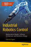
A circuit diagram of the input power section includes D C power management, a rectifier connected to A C voltage, and a battery. The D C power management contains safety controller, regulators and H V D C bus, 3 V 3, 5 V which further lead to motors and to electronics.
Input power section
DC Bus Voltage
The voltage of the DC bus depends on the application requirements and on the motors employed by the robot. A higher voltage level has the advantage of guaranteeing higher motor speeds and lower currents. However, it also poses more design challenges because of safety regulations. Large industrial robots typically hold their DC buses at several hundred volts. Smaller robots and the majority of hobbyist projects work at much lower levels (24V~60V) to simplify matters and avoid safety issues.
When working with high-voltage buses, a galvanic isolation between the low-voltage electronic circuits and the high-voltage section is important and often required by regulations. A typical example is an isolated gate driver that needs to keep the logic-level signals (including ground) separated from the switches side. The most common isolating solutions are optical (optocouplers), magnetic (integrated transformers), or capacitive. On the other hand, working at 60V DC or below is considered safe, and isolation is not needed.
The primary purpose of the DC bus voltage is to power motors, and therefore it needs to store enough energy to be able to respond quickly to any power request from the motors. The storage of energy is achieved by means of a large bulk capacitance. Typically, electrolytic capacitors are used because of their convenient capacitance-to-volume ratio. They do have quite a few drawbacks though: their actual capacitance value drifts over time; their shelf life is relatively short; their internal resistance is high, which means they dissipate significant power. However, nothing beats them when it comes to providing a large capacitance in a small amount of space and at a sensible price.
On a practical note, when designing the power stage for a motor driver, consider using many small capacitors in parallel instead of a single large one, because they are able to provide much higher instantaneous current levels, despite offering the same total capacitance.
One issue with having a large bulk capacitance is that a massive in-rush current is drawn when power is first applied at startup. The power supply is essentially shorted across a large empty charge reservoir to fill up: if no limitation is imposed, the initial current flow can be extremely high and damage the equipment. Also, it can cause the supply rails voltage to drop significantly, resulting in the entire system entering an undesired state and possibly affecting other subsystems powered by the same source. The solution is to introduce an in-rush current limiter to slowly pre-charge the capacitor bank, before the motor control stage is allowed to start up.


Two circuit diagrams. D C supply, current controller gate driver, C of bulk is highlighted in the first diagram and R of H m, C of bulk, current controller gate driver, and D C supply is highlighted in the second diagram. It depicts the two possible implementations of in-rush current limiters.
Two possible implementations of in-rush current limiters
In the second case, the junction temperature of the FET is monitored, and the device regulates the in-rush current to maintain the switch in its safe operation area. Regardless of the control mode, as more charge is stored in the bulk capacitors, the voltage difference between the power supply and the DC bus decreases. Eventually, when the Cbulk is fully charged, the switch is also fully open and opposes virtually no resistance to the flow of current needed to power the motors. This solution is relatively simple to implement, also considering that there are specialized chips on the market called hot-swap controllers, which integrate the gate driver and the current control together (e.g., LM5069 by TI).
The major drawback of this concept is that it requires a very large and expensive MOSFET, or more often a few of them in parallel, to allow the flow of enough energy to charge the bulk capacitors without burning out. In fact, the typical MOSFETs used in motor control bridges can sustain very high currents when fully conductive but perform very poorly when used in their high-resistive region (at low VGS, where RDS is high and a lot of power is dissipated into heat).

A graph of I subscript D versus V subscript D S plots 6 decreasing lines that falls down vertically with an equation limit R subscript D S on equals V subscript D S over I subscript D.
MOSFETs can operate at high VDS only for a very short amount of time
The pre-charge of very large capacitance can be accomplished using a slightly different circuit, shown on the right side of Figure 17-2. In this case, two N-channel MOSFETs are deployed in parallel, and they are both operated in their fully conductive region. One switch is activated first to let the in-rush current flow through an external power resistor, which is able to sustain large power losses for a longer time. Once the Cbulk is charged up, the second switch is turned on to provide a low-impedance path for the motor current.
As soon as the DC bus voltage reaches above a safe threshold, we can switch on the secondary buses and activate the main control electronics. Once the capacitors are fully charged, we can start driving the motors. Interestingly though, the motors are not mere passive loads: their movement has a strong influence on the DC bus voltage itself.
A motor is partly an inductive load (see model shown in Figure 14-1), which means that it stores energy in form of an electromagnetic field while running. This energy is provided by the bus capacitors during acceleration. The larger the motor and the higher its acceleration profile, the larger the power that the capacitors need to provide. If the charge stored in the capacitors is not enough, the DC bus voltage will drop.
During operation, the energy stored in the motor increases with its actual speed. On the other hand, when the motor slows down, that energy is released in electric form: the inductance forces a current out of the motor with an intensity dependent on the speed drop and on the deceleration time. In other words, if a motor running at high speed is forced to an immediate stop, a very large amount of energy is released into a powerful current burst. Conversely, if the motor slows down with a low deceleration profile, the same energy is released over a longer time window, causing a lower output current. Note that this effect does not occur with pure resistive loads (e.g., an LED) because no energy is stored in there.
Critically, the output current must be allowed to flow somewhere. During the deceleration phase, the bridge is essentially operating in reverse, i.e., trying to generate an induced magnetic flux pulling against the direction of movement of the permanent magnets. The result is that the excess current flows backward to the DC bus: the motor regenerates energy into the supply.

A photograph of a capacitor bank.
Capacitor bank on a DC bus shared between three motors
However, increasing capacitance comes with a few drawbacks: capacitors are expensive and take large space on the board; also, they need to be safely pre-charged with a current limiter, especially when many motor drives are connected in parallel on the same DC bus.
A shared DC bus across several drives is always a good option to consider: energy is shared between the axes, and general consumption is optimized. One decelerating motor can power an accelerating one. After all, motors in robots often all move at different speeds because of the nonlinearities of inverse kinematics.
Occasionally, even a large oversized bulk capacitance can fill up, and the excess charge needs to be absorbed somewhere else. If the system is powered by a battery (e.g., mobile robots, AGVs, electric vehicles, etc.), then the motor conveniently recharges the battery while slowing down. Electric cars take full advantage of this feature, which also significantly reduces wear on their mechanical braking system. Industrial robots, however, are rarely powered by batteries and often rely on fixed power supply units. In that case, the energy can either be fed back to the main electric grid (if the power supply is designed with such feature) or must be burned off quickly in form of heat. Other less common options consist in storing the regenerated energy in a supercapacitor or in a flywheel.

A schematic figure depicts the braking resistors and actual board implementation. R of power, C of bulk, R of e x t, D C bus are labeled in the first diagram, and power switch, gate driver, D C bus, C of bulk, R of power, and R of e x t are labeled in the board diagram.
Braking resistor schematic and actual board implementation
Figure 17-5 shows the practical implementation of a braking resistor control circuit for low-power applications. The resistor is an SMD type and allows a large power dissipation conducting heat away through the metal substrate of the PCB. An output connection is provided to add an additional external resistor to dissipate even more power for applications that require quick motor stops. The switch is a power MOSFET, which needs its own gate driver. The microcontroller constantly monitors the DC bus voltage level and activates the braking resistor by PWM switching. Typically, a simple proportional control loop is good enough to determine the duty cycle according to the excess overvoltage.
Pre-charge: This is part of normal operation, as the voltage rises while the bulk capacitance is being charged. The main electronic controller should be in sleep state until the available voltage reaches above a safe threshold.
Lack of power: This condition is typically caused by poor design. A sudden acceleration of all robot’s motors linked on the same bus causes a peak current to be drawn. If the bulk capacitors cannot supply enough energy, then the DC bus voltage will start dropping significantly. Voltage ripples are normal, but they should never dip too low. In that case, it would mean that the drives (or at least the capacitor bank) are undersized for the job. The solution is either to limit the movement dynamics or to redesign the drives with larger bulk capacitance.
Short circuit: An electric short somewhere on the wirings or internally in the motor can cause a voltage drop. The condition results in massive current being drawn from the power supply, and the safety functions should switch off the bridge immediately.
Protection Functions
When designing the power stage for any electric machine, we should always include a few safety features to make sure that nothing starts burning off. High voltage is significantly more critical to handle and requires its own set of regulations that we do not deal with here; low voltage can also result in hazardous situations for the devices, because the involved currents can still be quite high.
Reverse polarity: To prevent damage to the equipment when the user inadvertently applies the supply voltage at the wrong terminals
Circuit breaker: Should trigger when a short circuit at the output causes a large current to flow
Current limiter: Monitors the continuous average current to prevent overheating
Temperature monitor: To prevent overheating due to any reason
Reverse current block: (Optional) to prevent regenerating into a power supply
Over- and undervoltage: To make sure that the DC bus voltage does not exceed its safety range (as already described in the previous section)
Bleeder resistor: To provide a slow discharge path for the bulk capacitance after the system has been switched off
While there are integrated ICs that provide most of the listed functions into one single chip, they are usually limited to low-power applications. For high-power systems, as in the case of industrial robots, we need to implement a solution with several individual components.
Reverse polarity protection is probably the most basic requirement of any electronic system. Accidental wiring errors can always happen, and we should provide a way to avoid catastrophic and expensive consequences. Applying a negative voltage to the DC bus would cause the electrolytic capacitors to be reverse-biased, which results in damage and possible explosion. Technically, the reverse voltage across the bus would be initially clamped by the body diodes of the switches, which would conduct until they possibly burn down. In any case, a protection is needed.

A circuit diagram depicts a simple diode to block reverse polarity. The labeled parts in the circuit diagram are V subscript D C, V subscript f, I, and V subscript bus, and equation P equals V subscript f multiplied by I.
Using a simple diode to block reverse polarity is not an efficient solution

A circuit diagram depicts a M O S F E T for reverse polarity protection. The labeled parts are V subscript D C, I, D, G, S and V subscript bus.
A MOSFET is a more efficient choice for reverse polarity protection

A circuit diagram depicts an ideal diode controller. The parts labeled are S, D, G, I, V scubscript D C- positive and negative, and V subscript bus. It offers the lowest power loss.
Ideal diode: An N-channel device offers the lowest power loss

A flow diagram of V subscript bat, U P S, and main leads to 3 O Rings respectively, which further leads to the voltage output.
ORing controllers deployed for power redundancy architecture
Once we have guaranteed that the voltage is correctly applied to the DC bus, the second safety requirement we impose is to monitor the current flowing into the system and make sure that it does not exceed specific levels. We need to distinguish between continuous average current and peak current: a device can allow a nominal current to flow for an indefinite amount of time without overheating and ever needing to shut down; much higher peak current values are allowed, but only for very short bursts of time.
A simple fuse is always a sensible component to add in series to the power rail in order to prevent large current draws. However, besides being very cheap, it does not offer other advantages: it cannot perform very accurate current control, and it gets damaged when overcurrent occurs, requiring physical repair of the equipment.

A circuit diagram depicts the limited current flow through an e-fuse. The parts labeled are V subscript in, V subscript out, controller, and current sensing.
An e-fuse can accurately monitor and limit current flow without being damaged
The practical implementation of an e-fuse can either be realized with discrete components or even with integrated devices (e.g., TPS2595 by TI). Besides monitoring current, the device must also monitor the junction temperature of the FET, which should be typically kept below 150°C.
Actually, monitoring current flow should be done in both directions. We learned in the previous section that a decelerating motor can regenerate power into the DC bus and that the excess energy on the bus must be dissipated somewhere. Rechargeable batteries can naturally accept an input current (before they are fully charged), but standard AC-DC rectifiers cannot. We saw how braking resistors are the most common solution to this issue, but adding a protection to prevent unwanted current to flow back into the supply is also a good idea. Clearly, the reverse current protection is not needed if the power comes from a battery and regeneration can safely occur until the battery is fully charged (after that, the braking resistor will be forced to burn excess energy into heat).
Fortunately, the ideal diode solution implemented in Figure 17-8 also blocks reverse current. Note that the body diode of the switch is oriented from source to drain, so to block any regenerated reverse current even when the system is powered off, which can happen when the motors are forced to move by an external load.
One additional safety feature we need to consider is what happens to that massive electric energy stored in the DC bus capacitors as soon as the system is shut off. The bulk capacitance holds all the charge and keeps the voltage high. If someone were to open up the device to service it, a potentially dangerous voltage would still be present on the bus even if the power supply had been entirely disconnected.
For safety reasons, the DC bus capacitors must be discharged through a high-impedance path, called bleeder resistor. The resistor must be high enough to prevent quick discharge during normal operation but must be low enough to allow the DC bus voltage to drop below safe levels in a relative short time (i.e., 5 minutes) after the electric power has been shut off. That prevents danger to an operator accessing the equipment for service or repair, as long as the safety discharge time has elapsed.

A circuit diagram depicts the D C bus voltage monitor as a bleeder resistor. Resistor R 1 and R 2 are connected in series and parallel to capacitor C 1 and C bulk which leads to A D C.
The DC bus voltage monitor also serves as bleeder resistor
When power is switched off, the R1 + R2 series allows the charge stored in Cbulk to drain away in a reasonable time. The discharge rate of the initial capacitor voltage V0 through the resistive path R is given by the following:
 (17-2)
Example of discharge rate of bulk capacitor through bleeder resistor
Time [s] | 0 | 60 | 120 | 180 | 300 |
DC bus voltage [V] | 60 | 41 | 28 | 19 | 9 |
Usually, a bright warning sticker is placed on the outside case to act as a reminder: “Wait at least 3 to 5 minutes after disconnecting power before opening the device for maintenance.”
Voltage Converter
Besides the main DC bus voltage for the motors, we also need to provide a low-voltage supply for all the electronic controllers and other components in the system. Typically, most electronics work at either 5V or 3.3V, so we need a way to derive those values from the high-voltage DC bus.

Two circuit diagrams compare the switching regulator versus the linear regulator. Circuit diagram of linear regulator includes the components V in, V out, C in and C out. Switching regulator includes C boost and feedback connected to inductor L , V out, C out V out and diode D. V in and C in are connected at the beginning of the switching regulator.
Simplified schematics for linear regulator (left) vs. switching regulator (right)
Switching regulators, on the other hand, are much more complex devices that use an integrated PWM-controlled power switch to modulate output voltage in a closed-loop scheme. They are expensive, they require a large number of external components to be arranged with careful PCB layout, and they provide a noisy output voltage with non-negligible ripples, which can only be partially smoothed out with a large capacitor placed at their output. However, they are incredibly efficient and generate little power loss even at large voltage drops.

A circuit diagram of the D C bus of 60 volts, with a switching regulator of 12 volts and 2 linear regulators in series and gives output as M C U, and H M I, encoder with 3 V 3 and 5 volts respectively.
Combining switching and linear regulators for best efficiency
When selecting the voltage regulators, make sure that they can provide enough output current for the required application. Also, place generous copper area to allow for proper cooling.
Summary
Power management is the process of providing a stable and safe voltage source to all the system components, from the control electronics to the motors. Regardless of what energy source we use at the front end (either battery or AC supply), we need to generate a main DC bus, from which everything will be powered: the control system via DC/DC converters and the motors via the power switches in the inverters.
The power section is also the most critical in terms of safety functions, and a number of monitoring features must be built-in to guarantee safe operations in all circumstances. We described a few circuits to limit current and voltage to protect the system from hazards.