3
Changes in the Organization of the Earliest Microcomputers
This final chapter, which provides a partial conclusion to this volume, shows the evolution of the organization of the first microcomputers. From the earliest days of the microprocessor in 1971, there were evaluation boards such as the ones described in the previous chapter. Then, the microcomputer appeared, and the market for them exploded with the second generation (i.e. family version). Since the release of the Personal Computer (PC) in 1981 by IBM (International Business Machines Corporation), which refocused the PC for the business environment, motherboard architecture has not stopped evolving and taking advantage of the progress of integration in the domain of microelectronics. In particular, we saw the rise of the concept of the chipset. First, we will describe a second-generation microcomputer, the Apple II. Then, we will examine the evolution of the PC. The notion of chipset is elaborated. The architecture of modern motherboards is described. This chapter concludes with a discussion of low-level software from the firmware (FW) perspective.
NOTE.– The goal of this chapter is not to exhaustively describe the different architectures as would a specialized text about a particular model. It is to show the progression of architectures, even when focusing on a subsystem or a key feature.
3.1. Apple II
It is not possible to talk about the microcomputer without describing the Apple II as a worthy exemplar or as a support for the 2.0 or 2.5 generation of microprocessors (cf. § V3-4.3) or MPUs (MicroProcessor Units). It represents the first family microcomputers. Its motherboard (Figure 3.1) is a classic implementation from the era, based on TTL (Transistor–Transistor Logic, cf. § 2.3.2 in Darche (2004)) discrete logic circuits and LSI (Large-Scale Integration) circuits, including the MCS6502 MPU.
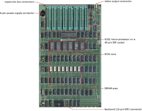
Figure 3.1. Original Apple II motherboard (Rev. 0). For a color version of this figure, see www.iste.co.uk/darche/microprocessor5.zip
The Printed Circuit Board (PCB) was made of (iconic green) FR4-type epoxy resin (Flame Retardant). The components used THT (Through-Hole Technology), which is analogous to the current SMC (Surface Mounted Component, cf. § 3.4.2) technology. With it appeared the extension connector “slot” designed to accept a daughter board, also referred to as an expansion slot, which sat perpendicular to the motherboard (eight available slots). Abundant discrete logic ensured the management (refresh, cf. § 5.2.2 in Darche (2012)) of DRAM (Dynamic Random Access Memory, shown in red in Figure 3.1), with a 48 KiB capacity (memory component reference 4116), and of the video display. The eight ROM (Read-Only Memory) components, each of which had a capacity of 2 KiB, are above the DRAM area. They contain a monitor (cf. § 2.2.4), a mini-assembler or disassembler, and a BASIC (Beginner’s All-purpose Symbolic Instruction Code) interpreter for whole numbers called Integer BASIC1 by its developer, Steve Wozniak (nicknamed Woz). The other integrated circuits are contained in DIP (DIL (Dual-In-Line) Package) 14- and 16-pin packages, providing glue logic (cf. § V3-2.3).
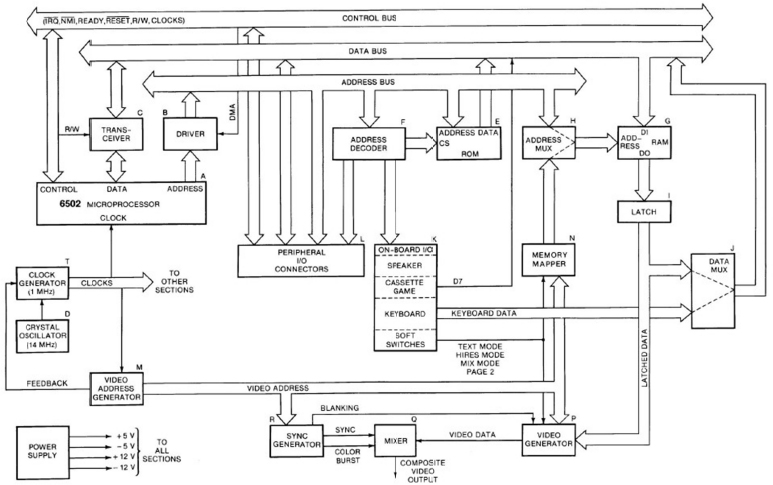
Figure 3.2. Apple II block diagram (Gayler 1983)
Figure 3.2 shows the general organization of this computer. The address and data bus signals (cf. Chapter 3) are simply amplified using 8T28 electronic buffers (cf. § 3.4.1 in Darche (2004)) for distribution to the expansion bus connectors.
In the expansion slot (Figure 3.3), we find the address, data and control bus signals for the MPU. Note the biphasic clock signals ϕ0/ϕ1. The electrical supply values for this generation were ±5 V and ±12 V (black power supply connector shown at the top left in Figure 3.1).
Figure 3.4 shows installed daughter boards. Note that insertion of a daughter board modified the electrical and temporal characteristics of the signals (cf. § V2-3.3 and V2-3.6). Given the clock speed of the MPU in this microcomputer, this had no effect on its operation.
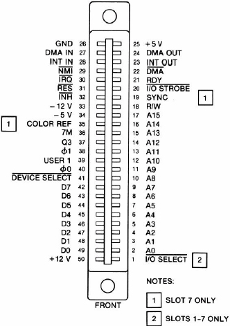
Figure 3.3. Top view of Apple II expansion slot (Gayler 1983)
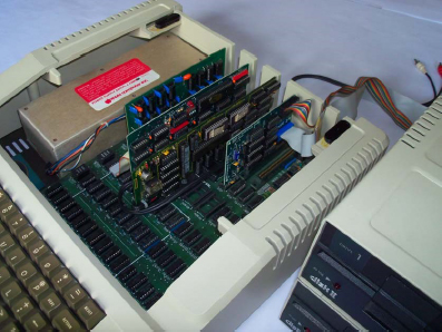
Figure 3.4. Installed daughter boards (unknown source). For a color version of this figure, see www.iste.co.uk/darche/microprocessor5.zip
An innovative feature was that all of the system’s clock signals, that is, the two signals from the 6502, DRAM refresh signals and video signals were generated from a master clock (f = 14.3 MHz). As a result, all of the subsystems that used them were synchronized. Dynamic memory was periodically swept to generate the video signal, which also refreshed it. This function constituted half of 1 μs MPU cycle, with the other half reserved for program execution. An oscillator built on an integrated NE555 timer circuit was responsible for modifying the video signal to make the cursor blink!
With regard to Input/Output (I/O), there was an interface for the keyboard, the speaker, the game port (joysticks and push buttons), and the audio tape recorder that provided mass storage (cf. § 7.2 in Darche (2003)). To read the voltage at the potentiometer terminals, the NE555 timer, generally used in monostable or astable mode, was adapted to create an Analog-to-Digital Converter (ADC). The software management routing was made responsible for this function. For more technical information, see Gayler (1983).
3.2. IBM PCs
The IBM professional line is the origin of the microcomputer, as we know it today. Three of their models made their mark on the IT industry. These were the 5150 (original PC), 5160 (XT) and 5170 (AT) models. We will now take a look at them.
3.2.1. The original PC
The Personal Computer (PC) was introduced by IBM in 1981. The history of this project at IBM is provided in Bradley (2011), Goth (2011), Bride (2011) and Singh (2011). Its open architecture is the foundation for modern microcomputers, which are referred to as “PC compatible”. It used the Intel 8088 MPU, which had a 16-bit internal architecture, an 8-bit external interface and a clock speed of 4.77 MHz. As with the Apple II, the clock speed was derived from a master oscillator running at 14.31818 MHz (divided by 3). The video signal (color burst) was obtained by dividing the same reference by 4.
It had a main memory capacity that ranged between 64 and 640 KiB (16 Ki x 1-bit DRAM reference 4116) and 40 KiB of ROM. The (EP)ROM ((Erasable Programmable) ROM) contained the BIOS (Basic Input/Output System), which included the Power-On Self-Test (POST, cf. § 3.5.3), the BASIC interpreter, the I/O routines, the 128-dot video pattern (i.e. ROM characters) and a bootstrap loader. The base RAM component was 16 Kib (type 4116). Each memory word had a format n of 9 bits, with the additional bit reserved for error detection via parity bit checking (EDC for Error-Detecting Circuit/Code). The controller alerted the user by generating an NMI (Non-Maskable Interrupt, cf. § V4-5.2) that enabled the display of a blocking message on the display. Figure 3.5 shows the motherboard.

Figure 3.5. IBM 5150 (original PC) motherboard. For a color version of this figure, see www.iste.co.uk/darche/microprocessor5.zip
Figure 3.6 describes the position of the components on the motherboard. The (V)LSI components include DMA controllers (DMAC for Direct Memory Access Controller, Intel 8237A), Programmable Interrupt Controllers (PIC, Intel 8259A), timers (Intel 8253), parallel I/O controllers and Programmable Peripheral Interface (PPI, Intel 8255A) controllers. Glue logic belonging to the TTL family surrounds the memory and these controllers.
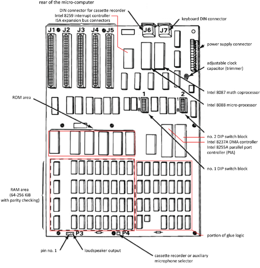
Figure 3.6. Overview of the IBM 5150 motherboard (IBM 1984a). For a color version of this figure, see www.iste.co.uk/darche/microprocessor5.zip
Five ISA (Industry Standard Architecture, cf. § V2-4.5) bus expansion slots made it possible to configure the machine for the user’s needs by selecting expansion cards. As in the Apple II, the signals on this bus are buffered signals from the MPU (cf. § 3.4.1 in Darche (2004)).
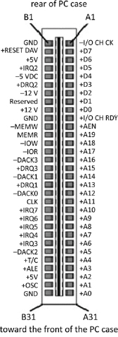
Figure 3.7. Overhead view of the 5150 bus expansion slot and its signals (IBM 1984a)
The bus contained at minimum a graphics card and a mass storage controller board. The display interface complied with the color CGA (Color/Graphics Adapter) standard, in other words, 320 x 200 in four colors selected from a palette of 16 colors, or monochrome. Note that a clock chip trimmer made it possible to adjust the master clock frequency (f = 14.31818 MHz) generated by the Intel 8284 circuit, which made it possible to match the display colors (at the time, a Cathode Ray Tube (CRT)) more precisely to the NTSC (National Television Standards Committee, f = 3.579545 MHz) color burst signal sent to a composite monitor. It contained two Floppy Disk Drives (FD for Floppy Disk and FDD for FD Drive, cf. § 7.2.2 in Darche (2003)) with a 5 1/4” format and a 3602 KiB capacity (double density format), from which the MS-DOS (MicroSoft Disk Operating System), which became the foundation for the first version of Windows, could be loaded. Note the presence of two circular DIN (Deutsches Institut für Normung) five-pin connectors (IEC 60130-9), which provided ports for an 88-key keyboard and a peripheral device, an external audio cassette recorder providing mass storage. This was a holdover from the first two generations of microcomputers and was subsequently abandoned.
3.2.2. The XT
The next model, which was released in 1983 (the IBM 5160), also called the PC/XT or just the XT (eXtended Technology), was an improved PC with the same MPU running at the same clock speed. Among the improvements were a Hard Disk Drive (HDD) with 10 MiB capacity in 5 1/4” format, which used an ST-506 parallel interface from Seagate. The number of expansion slots was increased from 5 to 8, and the RAM increased to 640 KiB, although each memory word kept the 9-bit format, for the same reasons as its predecessor. Figure 3.8 shows the motherboard. Note that a version containing a 286 microprocessor running at a clock speed of 6 MHz, with the reference number of 5162 (XT/286), was released in 1986.
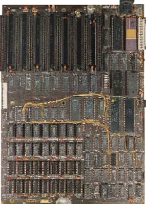
Figure 3.8. IBM 5160 motherboard (PC XT). For a color version of this figure, see www.iste.co.uk/darche/microprocessor5.zip
Figure 3.9 describes the position of the components on the motherboard. We can see there almost all of the same components that were in the original PC. However, the audio tape recorder interface was removed. The expansion slot signals were identical to the 5150, with the exception of the B8 pin, which carried the -CARD SLCTD (card selected) signal activated by a card (open collector type output, cf. § 2.3.2 in Darche (2004)) inserted into the J8 connector to indicate that it was selected (read only).

Figure 3.9. Overview of the PC XT motherboard (IBM 1983). For a color version of this figure, see www.iste.co.uk/darche/microprocessor5.zip
Note that, in this version of the machine, the POST (cf. § 3.5.3) is responsible for determining the RAM capacity. Previously, this was determined by reading a range of eight DIP switches (reference SW2).
3.2.3. The AT
One year after the XT, the IBM model 5170, also called the PC/AT or simply the AT (Advanced Technology), was architected around an 80286 microprocessor, a true 16-bit microprocessor clocked at 6 MHz, which made it possible to extend the address space to 16 MiB. Two addressing limitations existed with the preceding models. First, the limitation was physical, since the Intel 8088 microprocessor had an address bus size m of 20 bits (i.e. 20 address lines), which limited the address space to 1 MiB (= 220). The area between 640 KiB and 1 MiB was called the Upper Memory Area (UMA). Thanks to a memory management driver, it was possible to allocate Upper Memory Blocks (UMBs). The native Microsoft DOS (Disk Operating System) was therefore designed only to manage this conventional memory area. Additional memory belonging to this MiB could be used as a “RAM DISK”, in other words, as a mass storage to speed up access and to increase throughput. To enable a larger space, two approaches were implemented: expanded and extended memory.
The first, called augmented or expanded memory, used the bank or page switching approach3. The idea was to add a RAM area above this megabyte that was divided into pages of 16 KiB (=64 KiB), each with 16 KiB. The size varied from 4 MiB to 32 MiB depending on the model. Only a four-page frame was accessible between 832 KiB and 896 KiB. Note that this approach had already been implemented in the Apple II with 16 KiB pages (Saturn 128 KiB memory board). Four concurrent technologies were on the market: LIM, EMS, EEMS and XMA. The first was developed conjointly by Lotus Software, Intel and Microsoft, which based its acronym on the companies’ initials (EMS 3.0 – 1985). The Expanded Memory Specification (EMS) 3.2 was released in September of the same year and offered a memory space of up to 8 MiB (4 pages of 16 KiB). A software manager called EMM.sys (Expanded Memory Manager) needed to be added to the OS in the form of a driver. Subsequently, a version of the specification called EEMS (Enhanced Expanded Memory Specification), proposed by Ashton-Tate Research, Inc. (AST; for the initials of founders Albert Wong, Safi Qureshey and Thomas Yuen) and Quadram, extended the window to 64 pages. The latter was incorporated into LIM EMS 4.0 (August 1987), which offered up to 32 MiB of expanded memory. In 1986, IBM proposed its own specification using the acronym XMA (eXpanded Memory Adapter) for its expansion board, which offered 2 MiB of memory.
With the release of MPUs with greater physical address space, such as the 16 MiB (=224 bytes4) available in the Intel 80286 and 386SX and the 4 GiB (= 232 bytes) in the 80386, the previous technique became obsolete. Memory above the first MiB was still called “extended memory” for the purpose of distinguishing this first 1 MiB of space from the rest of the memory. The associated technology, called XMS (eXtended Memory Specification), was proposed by the LIM Association and AST Research. Version 2.0 was published in July 1988, and 3.0 was released in January 1991. The first 65520 (= 216 – 16) bytes of extended memory accessible in real addressing mode4 formed the High Memory Area (HMA). This range is the result of the difference in the management of the address space ranging from FFFF:0010 to FFFF:FFFF in the 80286 MPU compared to the 8088/86, since the latter could not go beyond a MiB. Figure 3.10 maps the PC memory space (concept explained in § 2.6.3 in Darche (2012)).
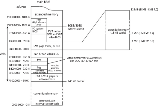
Figure 3.10. Topography of main memory (Figure 2.110 in Darche (2012) completed)
Figure 3.11 shows an AT type 1 motherboard.

Figure 3.11. IBM 5170 type 1 motherboard (PC AT). For a color version of this figure, see www.iste.co.uk/darche/microprocessor5.zip
Figure 3.12 shows the position of the components on the printed circuit. Main RAM was composed of four banks of 9 DRAM, reference 41128, with a unit capacity of 128 Kib.
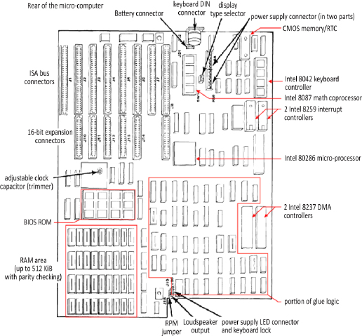
Figure 3.12. Overview of the PC AT type 1 motherboard (IBM 1984b). For a color version of this figure, see www.iste.co.uk/darche/microprocessor5.zip
The type 2 motherboard was narrower (Figure 3.13) thanks, particularly, to the reduction of the DRAM to two banks of 41256 integrated circuits (256 Kib).

Figure 3.13. Overview of the PC AT type 2 motherboard (IBM 1986). For a color version of this figure, see www.iste.co.uk/darche/microprocessor5.zip
The ISA (Industry Standard Architecture) bus expansion format was extended to 16 bits using the name “AT bus”, thanks to the addition of a second connector (a shorter extension from the first connector), which thus enabled upward compatibility with the ISA bus. Figure 3.14 shows its signals.

Figure 3.14. ISA bus expansion slot extended to 16 bits and its 16-bit expansion signals (seen from above)
Figure 3.15 shows the organization of this microcomputer. Electronic buffers amplify the MPU’s signals on the bus to distribute them to the expansion slots. They can also be bidirectional.

Figure 3.15. AT block diagram (IBM 1984b)
The capacity of the Floppy Disk (FD), which retained its flexible, square cartridge (i.e. enclosure), increased to 1.2 MiB (high density) in the same format as the XT. The hard disk drive unit, still in 5 1/4” format, increased to a 20 MiB capacity. Processing power increased by a factor of 4 compared to the XT (0.8 compared to 0.2 MIPS, cf. § V4-3.4 for the unit of performance measurement).
3.3. Chipset
With progress in integration, glue logic around the MPU, memory subsystems and I/O controllers were integrated into VLSI (Very LSI) chips, with the whole being called a chipset. After defining this component, the PC architectures that use it will be described.
NOTE.– This study runs until around the year 2000, and will be completed in subsequent works.
3.3.1. Definition
A chip set integrates digital logic circuits around the microprocessor (address decoding, etc.) and the I/O controllers into a set of integrated circuits. It is associated with a microprocessor and an expansion bus and is bundled with the various microcomputer architectures. It plays an essential role in the computer’s performance. The manufacturers were most often those who built microprocessors (AMD, Intel, etc.), but there were other precursor companies (Chips & Technologies, VIA Technologies, ZyMOS, etc.) Three generations can be identified.
The first generation, around the year 1990, was a first step in the effort to integrate everything by bringing together the glue logic and the various memory and I/O controllers using the technology of the time. It began with the 80286 and continued into the 80386 and 80486 microprocessors. It used an ISA (Industry Standard Architecture) expansion bus. The term “chipset” was fully realized with, in general, at least four VLSI (Very Large-Scale Integration) chips. The circuits were made under license from Intel.
An example was the POACH (PC-On-A-Chip) family, the ASIC (ApplicationSpecific Integrated Circuit) using CHMOS (Complementary High-density MOS (Metal-Oxide Semiconductor)) from ZyMOS (announced at the end of 1985), with three 84-pin packages.
The 82C230 circuit (POACH1) primarily integrated the 82284 clock signal generator, the two 8259 PICs, the MC6818 (BB-)RTC ((Battery-Backed) Real-Time Clock)/ CMOS (Complementary MOS) memory5, the 82288 bus controller and the glue logic associated with the bus.
The 82C231 circuit (POACH2) primarily integrated two 8237 DMACs (Direct Memory Access Controllers), an 8284 clock signal generator, an 8254 clock/timer, the refresh and error control logic for dynamic RAM and logic connected to I/O. These two components replaced 12 LSI components.
The 82C232 circuit (POACH-3) integrated additional discrete logic connected to buffering (cf. § 3.4.1 in Darche (2004)) of addresses and data, equivalent to seven LSI components. A use case for this set is the CCAT (Circuit Cellar AT) described in Ciarcia (1987a, 1987b).
Chips and Technologies (C&T) is another company that made a mark in this area with its chip sets. Among others, it produced the 82C206, a component that was part of the CS8221 CHIPSet™ called the New Enhanced AT (NEAT™). The 82C206 integrated the I/O controllers (Integrated Peripherals Controller) for DMA transfer, interrupts and timing (timer and RTC), which was missing from the previous CS8220 chipset. The final chipset was named the 82C836 Single-Chip AT (SCAT™), which integrated the preceding components.
In November 1992, Intel announced the 8240 TX/EX/ZX chipset for the 486 family under the name PCIset, with the code names of Saturn, Aries and Saturn II, in which the first intended for this expansion bus. It consisted of three components: the 82424TX Cache and DRAM Controller (CDC), the 82423TX Data Path Unit (DPU) and the 823781IB System I/O or SIO (Figure 3.16).
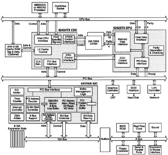
Figure 3.16. Architecture based on the 82420 chipset for use with the 80486 (Slater 1992) © The Linley Group
The DPU connected the host (i.e. MPU bus) and PCI buses. The SIO enabled the connection between the original ISA (Industry Standard Architecture) bus to a generic bus with a higher throughput; in other words, one that was independent of the MPU, called the PCI, for Peripheral Component Interconnect (PCI-SIG 1998, cf. § V2-4.2.4). Version 1.0 of the specification is dated June 1992, and version 2.0 is from April 1994. With this second generation of chipsets, we can see motherboard architecture transitioning from ISA to PCI expansion buses. This bus hierarchy (cf. § V2-4.1) makes it possible to adapt to the throughputs of the various subsystems.
The host bus is the fast bus because it is the bus for the MPU, as well as the cache and DRAM subsystem. The PCI expansion bus receives the fastest I/O cards, which are the video adapter, the SCSI (Small Computer Systems Interface, cf. § 9.3.1 in Darche (2003)) and the network interface. The X-bus connected to the ISA expansion slots connected to the older, slower PC components such as the BIOS ROM, the RTC, and the keyboard, parallel and serial interfaces, and FDD controllers. This hierarchy also made it possible to move progressively to the next generation expansion bus while keeping one or two connectors from the previous bus. We begin here to see two logical subsystems referred to as north and south based on their position in this figure. The north logic is in contact with the MPU and manages the DRAM (refresh and access) and the cache. It enables the link between the local bus and the first expansion bus. The south subsystem provides the bridge between the expansion buses.
The 430LX family (code name Mercury), announced at the beginning of 1993, was notable for the P5 architecture, the first MPUs for which were the 60 and 66 MHz Pentium6 chips. Figure 3.17 shows an architecture using it. This family’s organization is similar to the previous one. We see the PCI, Cache and Memory Controller (PCMC, reference 82434), a memory interface or Local Bus Accelerator referred to as LBX, with a reference number of 82433. Level 2 (L2) cache memory is now integrated. Cache placement policy uses direct mapping (this will be covered in a future book by the author on memories). I/O management is left to the System I/O (reference 82378ZB).
This chipset could be easily adapted to another expansion bus such as Extended ISA (EISA). The SIO was replaced by two components, the 82375EB PCEB (PCI/EISA Bridge) and the 82374EB ESC (EISA System Component). Figure 3.18 shows a motherboard architecture that implements this configuration.
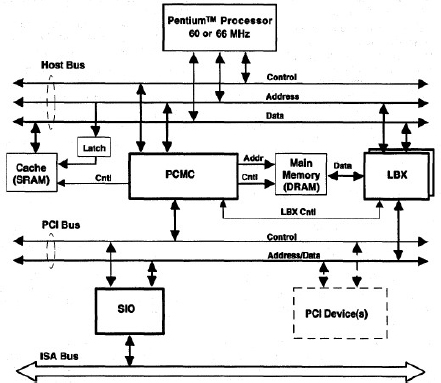
Figure 3.17. Architecture based on the 82430 chipset for use with the Pentium (Intel 1993)

Figure 3.18. Components in the 82430 chipset managing the EISA (Gwennap 1993) © The Linley Group
Table 3.1 compares the main characteristics of the 430 family of chipsets. The 430LX only uses FPM (Fast Page Mode) type DRAM. The Triton family introduced the use of EDO (Extended Data Out) type DRAM. Note the use of a synchronous version (SDRAM, with the S standing for Synchronous). These three memory architectures are studied respectively in § 5.5.2 in Darche (2012) and in Chapter 6 of this same work. The AGP (Accelerated Graphics Port) bus is not supported.
Table 3.1. Characteristics of Intel 430 chipset family (except for the mobile 430MX version)
| References | ||||||
|---|---|---|---|---|---|---|
| Characteristics | 430LX | 430NX | 430FX | 430HX | 430VX | 430TX |
| Year | March 1993 | March 1994 | January 1995 | February 1996 | February 1996 | February 1997 |
| Code name | Mercury | Neptune | Triton | Triton II | Triton II | - |
| Microprocessor | Pentium P60/66 | Pentium P75+ | Pentium P75+ | Pentium P75+ | Pentium P75+ | Pentium P75+ |
| Multiprocessing | No | Yes | No | Yes | No | No |
| Memory type | FPM | FPM | FPM, EDO | FPM, EDO | FPM, EDO, SDRAM | FPM, EDO, SDRAM |
| Address capacity (MiB) | 2–192 | 2–512 | 4–128 | 4–512 | 4–128 | 4–256 |
To the north and south bridges was added a component called a Super I/O or Ultra I/O™7 chip, integrating all of the PC’s traditional I/O controllers. Historically, it was connected to the ISA (Industry Standard Architecture) bus (Figure 3.19), then later to an LPC bus (Low Pin Count, cf. below). Then, it was integrated naturally into the south chipset. Monochip solutions integrating north/south and super I/O chipsets were proposed, such as the one from SiS, with the reference number Sis 630/73x.

Figure 3.19. Internal overview of a super I/O component: the PC87306 from NS
With the Pentium Pro, II and III came the 440 and 450 families. The 440FX PCIset, code named Natoma, designed for the P6 architecture (Pentium Pro and Pentium II), was announced in May 1996. Before that, in November 1995, the 450KX/GX (respective code names Mars and Orion) for the Pentium Pro were released. As an aside, these three MPUs had two external and independent local buses, also called system buses, which were referred to respectively as the Back-Side Bus (BSB) and the Front-Side Bus (FSB). The BSB linked the microprocessor to the cache-type memory buffer (cf. a future sequel to Darche (2012)). The FSB or host bus is connected to the HUB or bridge, which is the real communications hub between all of these subsystems. Intel called this architecture the Dual Independent Bus (DIB, cf. § V2-4.2).

Figure 3.20. Organization of a motherboard with an Intel 450KX/GX chipset (Intel 1996)
Figure 3.20 shows an example multi-MPU application. The KX version supported up to two processors on the host bus, with one dynamic Memory Controller (MC) and one host-to-PCI Bridge (PB) that connected the host bus to the PCI expansion bus. The GX version could manage up to four processors, two memory controllers and two PCI buses (grayed-out section indicates the difference between the two versions). The MC included an 82453KX DRAM Controller (DC), an 82452KX Data Path (DP) with four 82451 Memory Interface Components (MIC) per MC.
Version 2.0 of the 440LX/EX/BX added AGP support for the first time, as did the ZX a few months later in the same year. Figure 3.21 shows an example implementation. The 440 EX is a low-cost version of the 440LX designed for the Celeron family.

Figure 3.21. Implementation of AGP with the 440BX chipset (source: Intel)
Tables 3.2 and 3.3 recap the primary characteristics of the first chipsets for the 44x and 45x families.
Table 3.2. Characteristics of the first Intel chipsets in the 450/440 families
| References | |||
|---|---|---|---|
| Characteristics | 450KX | 450GX | 440FX |
| Year | November 1995 | May 1996 | |
| Code name | Mars | Orion | Natoma |
| Microprocessor | Pentium Pro | Pentium Pro and II | |
| Multiprocessing | Yes | ||
| Memory type | FPM | FPM, EDO and BEDO | |
| Maximum addressing capacity | 1 GiB | 8 GiB | 1 GiB |
Table 3.3. Characteristics of the first Intel chipsets in the 450/440 families (continued from Table 3.2)
| References | |||||
|---|---|---|---|---|---|
| Characteristics | 440LX | 440EX | 440BX | 440GX | 450NX |
| Year | February 1996 | April 1998 | June 1998 | ||
| Code name | Balboa | - | Seattle | - | - |
| Microprocessor | Pentium II and Celeron | Pentium II and Celeron | Pentium II, III and Xeon | ||
| Multiprocessing | Yes | No | Yes | ||
| Memory type | FPM, EDO and SDRAM | EDO and SDRAM | SDRAM | FPM and EDO | |
| Maximum addressing capacity | 1 GiB in EDO 512 MiB in SDRAM | 256 MiB | 512 MiB | 2 GiB | 8 GiB |
With the third generation, the meaning of the term “chip set” evolved. It now refers to the component and not to the set to which it belonged. The number of chips in the chipset was reduced to 2 + 1. We now speak about north and south chipsets. Intel introduced the Intel Hub Architecture (HUB IHA), also known as the Accelerated Hub Architecture (AHA) under the i8xx reference number, with the first being the i810 in 1999 for use with the Pentium III and Celeron chips in a socket 370 (PGA370 socket), referred to by the code name Whitney. The chipsets or bridges, the north bridge and south bridge, were respectively called the Memory Controller Hub (MCH) and the I/O Controller Hub (ICH), as shown in Figure 3.22.
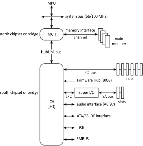
Figure 3.22. Intel HUB architecture
It should be noted that a graphics controller could be integrated (IGP for Integrated Graphics Processor) in the north bridge, which made it possible to manage a single system/graphics memory area called the Frame Buffer (FB). It was referred to using the acronym GMCH for Graphics and Memory Controller HUB.
Main memory was therefore partitioned, statically or dynamically, in order to share it between the microprocessor and the display controller. This is what was called the Unified Memory Architecture (UMA, will be covered in a future book by the author on memories).
The two bridges communicate via a fast, proprietary, point-to-point interface called the HubLink or HL (Ajanovic and Harriman 2000). A new interface in the I/O controller hub, called LPC, replaced the traditional ISA (Industry Standard Architecture) and X-bus standards. A third component called a Firmware Hub (FWH) included flash memory for the BIOS and a Random Number Generator (RNG) under the 82802 reference number.
The 820 family was released in November 1999 and supported version 4.0 of the AGP standard. DRDRAM memory, designed by Rambus (Direct Rambus DRAM), was supported for the first time in the PC800 version (cf. § 7.2.1 in Darche (2012)), which was a failed attempt by Intel to introduce this high-performance but expensive architecture. For the Pentium 4, Intel offered the same architecture in the 8xx series, released in the following order: 850, 845, 875, 865 and 848 (first components). The 850 (code name Tehama) managed PC600/800 RDRAM, but the 845 returned to SDRAM.
The Direct Media Interface (DMI) is a high-speed bus first used in the Intel 9xx series in 2004 to connect the MCH and the ICH (Figure 3.23). The bus had four bidirectional channels, with the exception of some mobile versions, which only had two channels.
The architecture that superseded IHA was called PCH (Platform Controller Hub), which was introduced in 2008. By integrating the functions of the north bridge into the MPU, the chipset was reduced to one chip responsible for I/O, the ICH. This was the fourth generation. The first family was called the series 5. The PCH was connected to the ICH through the fast DMI interface used in the preceding architecture.
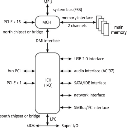
Figure 3.23. DMI link connecting the MCH to the ICH: the 915P
AMD used a similar technology called LDT (Lightning Data Transport), which was renamed HyperTransport (HT) in 2001 and subsequently managed by a consortium of the same name. Among others, the founding members included Apple Computer, Broadcom Corporation, NVIDIA and Sun Microsystems. LDT was a fast, bidirectional, point-to-point connection called a link between integrated circuits, which made it possible, for example, to connect an MPU to its I/O hub (i.e. the south chipset) via a component called a tunnel that contained a bridge, as shown in Figure 3.24, allowing for communication with the PCI-E bus. In addition to the bridge with tunnel, there were three other configurations – simple link, tunnel and tunnel-less bridge. The link format varied from 2 to 32 bits (growth factors of 2). The electronics used differential logic called Low-Voltage Differential Signaling (LVDS, cf. § 2.8 (Darche 2004) and § 3.4 (Darche 2012)), in a 1.2V version. This technology was notably used by AMD in its 64-bit MPUs (Opteron and Athlon). For more information about this bus, refer to § V2-4.4 and (Trodden and Anderson 2003; Holden et al. 2008).
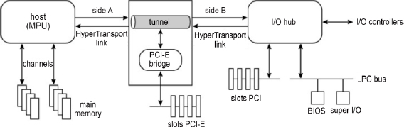
Figure 3.24. HyperTransport Tunnel
3.4. Motherboard architectures
The earliest models were produced by IBM. These were the original PC, the XT, and the AT, which used discrete logic. These were followed by the models described in this section. Different motherboard generations followed the chipsets (cf. § 3.3), which followed the MPUs, with variations depending on the Integrated Circuit (IC) package, which was housed in a support called a socket.
3.4.1. Form factors
In the world of PC compatibles, form factor refers to the mechanical characteristics of the motherboards in the first three IBM microcomputers (PC, XT and AT). Later, variants appeared (Figure 3.25). For example, the “full AT” became the Baby-AT, and then the ATX (Advanced Technology eXtended), which had the same form factor as the Baby-AT but was turned 90°. We should also mention the LPX (Low Profile eXtended or eXtension), NLX (New Low profile eXtended) and WTX (WorkStation eXtended) form factors. The BTX (Balanced Technology eXtended) form factor was released in September 2003. These form factors also apply to the motherboard power supply and to the outer case.

Figure 3.25. Timeline of the main motherboard form factors
Table 3.4 details the dimensions of the different motherboard form factors with the corresponding MPUs.
Table 3.4. Summary of various form factors
| Models | Ranges | Year | Origin | Length (mm/inch) | Width (mm/inch) | MPU |
|---|---|---|---|---|---|---|
| Original PC (5150) | 1981 | IBM | 279/11 | 216/8.5 | Intel 8088 | |
| XT (5160) | 1983 | IBM | 305/12 | 216/8.5 | Intel 8088 | |
| AT (5170) | type 1 | 1984 | IBM | 350/13.8 | 305/12 | Intel 286 |
| types 2 and 3 | 1985 | IBM | 350/13.8 | 236/9.3 | Intel 286 | |
| Baby-AT(XT-286) | 1985 | IBM | 254–330/10–13 | 217/8.57 | Intel 286/386/486 | |
| LPX | 1987 | Western Digital | 330/13 | 229/9 | Intel 286/386/486 | |
| mini-LPX | Western Digital | |||||
| NLX | 1996 | Intel | 254–345/10–13.6 | 203–229/8–9 | ||
| ATX | 1996 | Intel | 305/12 | 244/9.6 | Intel Pentium | |
| mini-ATX | AOpen Inc. | 150/5.9 | 150/5.9 | Intel Pentium | ||
| mini-ATX | 1997 | Intel | 284/11.2 | 208/8.2 | Intel Pentium | |
| microATX | 1998 | Intel | 244/9.6 | 244/9.6 | Intel Pentium | |
| Flex-ATX | 1999 | Intel | 229/9 | 191/7.5 | Intel Pentium | |
| WTX | 1998 | Intel | 425/16.75 | 356/14 | Intel Pentium | |
| ITX | 2001 | VIA | 215/8.5 | 191/7.5 | VIA/x86 | |
| mini-ITX | 2002 | VIA | 170/6.7 | 170/6.7 | VIA/x86 | |
| nano-ITX | 2003 | VIA | 120/4.7 | 120/4.7 | VIA/x86 | |
| BTX | 2003 | Intel | 325/12.8 | 267/10.5 | Intel Pentium | |
| microBTX | 2003 | Intel | 267/10.5 | 264/10.4 | Intel Pentium | |
| nanoBTX | 2004 | Intel | 267/10.5 | 223.5/8.8 | Intel Pentium | |
| picoBTX | 2003 | Intel | 267/10.5 | 203/8 | Intel Pentium | |
| DTX | 2007 | AMD | 203/8 | 244/9.6 | x86 | |
| Mini-DTX | 2007 | AMD | 203/8 | 170/6.7 | x86 | |
| NUC | 2012 | Intel | 10/4 | 10/4 | Intel |
3.4.2. Current motherboard architecture
Figure 3.26 shows the motherboard for a contemporary microcomputer with the microATX form factor. With a few exceptions such as the power supply connectors, the components are all surface mounted (SMD for Surface-Mounted Device), which is associated with SMT (Surface Mount Technology). The main component is the microprocessor, here a Core™. Only its Zero Insertion Force (ZIF) socket is shown. The second subsystem is the RAM, made up of four 2400 MHz DDR4 (Double Data Rate, cf. § 6.5 (Darche 2012)) DIMMs (Dual-In-line Memory Modules), inserted into memory slots. In comparison to the first PC, what is remarkable is the disappearance of the glue logic that enabled management of and communication with memory; the I/O exchange units have also disappeared in favor of a single B250 south chipset, with the north chipset being integrated into the MPU. However, it is surrounded by numerous components that supply the MPU with power (radial capacitors and coils). The GPU (Graphics Processing Unit) is integrated into the MPU.

Figure 3.26. Current PRIME B250-PRO motherboard (source: Asus – 2018, completed). For a color version of this figure, see www.iste.co.uk/darche/microprocessor5.zip
The I/O connectors are found on the side of the motherboard that touches the back of the computer case. It connects to external peripherals. Other connectors distributed on the other sides make it possible to either connect a mass storage unit or complement the rear connectors by allowing them to be moved to the front or rear side of the case.
3.5. Evolution of microcomputer firmware
At startup, all computers require a program stored in ROM called firmware. Three companies have made their mark with their firmware: Apple, IBM and Sun. They are described after a precise definition of the term.
3.5.1. Definition
Historically, the term is attributed to Acher Opler from an article in Datamation magazine in January 1967 (Opler 1967). Firmware (FW) or micrologic is the low-level logic that controls a microprocessor-based system, at least on startup. It is stored in non-volatile memory (ROM) or potentially (during operation) in RAM (shadow BIOS, cf. § 3.5.3), as opposed to software (SW), which designates the set of programs stored in storage devices. For a computer, it is responsible for hardware (HW) testing, initialization and configuration, and for loading the OS. It is also an interface between the hardware and the OS. It can also provide interactive debugging functionality.
3.5.2. Apple II
Two programs, a resident system monitor and the BASIC interpreter, were installed on the motherboard. They were written by Steve Wozniak.
3.5.2.1. The system monitor
The Apple II had a ROM-resident system monitor (cf. § 2.2.4). There was a text editor and a so-called self-prompting command interpreter; in other words, it waited for input of one of 22 provided commands in the form of a letter. This firmware made it possible to read and disassemble memory, to assemble (mini-assembler) a program, to write, move or compare a block, and to load and launch execution of a program at a given address. It also enabled reading and writing from a cassette tape. Debugging commands made it possible to examine and modify the MPU 6502’s registers, among other actions.
3.5.2.2. BASIC ROM
The firmware also included a BASIC language interpreter that was launched either manually or automatically depending on the version (Autostart ROM).
3.5.3. PC BIOS
In the early days of computing, applications directly managed input–output and used specialized libraries. The invention of operating systems allowed them to offload this management. The advent of the microcomputer with the CP/M operating system (Control Program for Microcomputers from Digital Research) introduced the notion of a BIOS, which allowed the OS, which was called BDOS (Basic Disk Operating System), to rely on a software layer for input/output management (Figure 3.27a).
The BIOS was primarily designed for disk management. Services were launched by calls from subprograms. The PC with DOS (Disk Operating System) popularized this principle. However, calling these routines was done by software or hardware interrupt (cf. § V4-5.1), and the processor’s registers were used to pass incoming and outgoing parameters. Originally kept in secondary memory for CP/M, the BIOS for the PC was moved to ROM on the motherboard. The BIOS (Basic Input/Output System) is therefore software stored in ROM (firmware). It dates back to the first PC (1981). It was difficult to build for because it had never been officially specified; the only reference document was IBM’s hardware reference manual (IBM 1981, 1984). It was specifically designed for the x86 architecture (processors and related circuits – I/O controllers). At initialization, the MPU connected to the reset vector (= FFF016) address. An unconditional jump instruction labeled RESET was stored there, at the beginning of the BIOS with the POST program.
This is why BIOS is found at the top of the address space (Figure 3.27b). It executes in real-time, that is, there is no management of virtual memory, and the memory area, which is limited to 640 KiB (!), is not protected. As a result of the limitations of this approach, an application can directly use a BIOS routine by bypassing the OS, and can even directly manage hardware (in the case of game software). Indeed, the two previously mentioned OSes were single task/single user, and an application could indefinitely lock up the computer, for example by hiding interrupts.
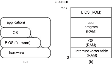
Figure 3.27. The different functional layers of an old-generation PC microcomputer and a diagram of main memory for the original PC (1981)
The BIOS provides three essential functions: Power-On Self-Test (POST), hardware initialization and first-level loading. It also provides an interface between the OS and the hardware in the form of Interrupt Service Routines (ISR). The final program, for configuration (setup), is not present on every machine.
The POST for the original PC ran a hardware diagnostic to detect malfunctions. At startup, it tested the MPU, the main memory, the BIOS and the DRAM. The MPU test examined flags and associated conditional jumps, as well as the other registers. The test for the ROM that contained the BIOS was based on a checksum (cf. III.6.4 in Darche (2000)). The DMA controller was then tested and initialized in order to refresh the DRAM. The first 32 KiB of DRAM was then tested by reading and writing a 5-byte sequence (base 16) that consisted of AA, 55, FF, 01 and 00. The 8259 interrupt controller was then initialized, as was the interrupt vector table (cf. § V4-5.7). The video controller was initialized. The IT controller was then tested. The keyboard was tested. Testing the RAM above 32 KiB then continued by calculating its total size. There could also be additional BIOS at the interface-board level (range of C8000:F400016 by 2 KiB block), whose presence was indicated by signing the first two bytes 55AA16. It was detected and then tested. The program determined whether a floppy disk drive was attached and, if so, loaded the primary bootstrap loader found on the disk. Note that in modern computers, the primary boot loader is found in general in the first sector (no. 1) of the first track (no. 0), called the MBR (Master Boot Record) on the primary hard drive’s active partition. The boot sequence consists of finding the OS, loading it and transferring control to it. The function of the primary boot loader is to find the secondary boot(strap) loader, which will then finally load the operating system.
The setup program specifically allowed the date and time to be adjusted, as well as the boot priority order for the mass storage devices. For more details on the BIOS, see, for example, Croucher (2004).
Since ROM access time8 is slower than RAM access time, the BIOS can be transferred when the machine is initialized to improve execution time for internal routines. This technique is called shadow BIOS. A microcomputer can have a dual BIOS, referred to as the primary and secondary BIOS. During the initialization sequence, the primary BIOS is tested, for example using a checksum or a Cyclic Redundancy Check (CRC), described respectively in § III.6.4 and III.6.7 in Darche (2000); also cf. § 2.6.4 in Darche (2012). If the test is negative, the secondary BIOS is selected and tested. If this test is negative, the machine is halted. This technique makes it possible, among other things, to recover the machine in the case of a failed firmware update. The flow chart is presented in Noll (1998).
The BIOS is fixed and proprietary. The binary image, once generated, cannot be changed. It is executed in real-time mode with an address limitation of 1 MiB. To resolve this situation, Intel proposed a new version called EFI (Extensible Firmware Interface), which is described in Intel (2000), initially called the Intel Boot Initiative or IBI (1997) and designed for the Itanium architecture. This was a standardized and independent interface between the motherboard’s firmware and the OS (Figure 3.28) that also provided an Application Programming Interface (API). Thus, the OS was allowed to launch and take charge of the underlying hardware such as mass storage, network or display interfaces. It was written in a modular fashion in a High-Level programming Language (HLL), the C language being most suitable, and not in assembly language, as is the BIOS, to facilitate development, maintenance, updating and portability.
This architecture provides a shell for launching setup and diagnostic utilities. The initialization phase for the BIOS remained unchanged. It managed all of the mass storage devices as well as the network interfaces. It also had an expansion mechanism that allowed it to adapt to new peripherals. It also managed drivers.
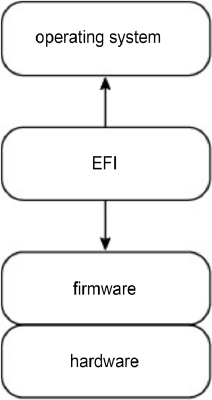
Figure 3.28. EFI software location
Unified EFI (UEFI) succeeded EFI and is supported by an association founded in 2005, whose members include several hundred companies, including Intel and Microsoft. It supports non-Intel architectures such as Arm®. Its specification is almost 3,000 pages long (UEFI 2017).
Originally, the BIOS could not be updated because it was stored in ROM. EPROM (Erasable PROM) technology made it possible to program the ROM electrically using an external programmer, with erasing being done using ultraviolet light (for more on this subject, cf. § 2.1.2). Today, non-volatile memory (NVM) is programmable and erasable electrically (Flash EEPROM/E2PROM for Electrically EPROM or FEEPROM/FE2PROM). Programming is carried out using a memory dump in the form of a file stored locally, originally on a disk and later on a local or even a remote storage device. Firmware for the most well-known PCs came from AMI (American Megatrends, Inc.) and Phoenix Technologies.
Additional information is found in Dice (2018).
ADDITIONAL INFORMATION.– BSP (Board Support Package) is low-level firmware designed for an embedded system (the original source of the term). It sits between the hardware and the OS. It provides hardware abstraction for the OS by converting its generic function calls into I/O routines. Its functions, in order of definition, are initialization, boot, hardware management (drivers) and interrupt management. It may contain information files concerning the board hardware. The IBM PC BIOS can be seen as its forerunner.
3.5.4. Open firmware
Sun workstations had a monitor residing in PROM (Programmable Read-Only Memory) called open firmware, also called OpenBoot, originally developed by Sun. This firmware is hardware independent. It was standardized by the IEEE under reference number IEEE Std 1276-1994 (IEEE 1994a, 1994b, 1994c, 1995). It enabled subsystem diagnostics (POST) on startup, including the keyboard, main memory, the mass storage devices, the I/O controllers, etc. It could also be launched during startup of the computer to allow for management commands to be entered from an interpreter. It was initially used in Sun workstations designed around an MPU from the SPARC (Scalable Processor ARChitecture) family and in PowerPC-based Macintosh computers.
3.6. Conclusion
We have described the architecture of the first emblematic microcomputers, the Apple II and the various generations of the PC. The latter were architected around a chipset. These chipsets were then presented. What this chapter has shown is the progressive integration of discrete logic components, and then subsystems, to arrive at a single component that is peripheral to the MPU and main memory. Then, to conclude the chapter, the firmware aspect was addressed by presenting the PC’s BIOS and (U)EFI.
- 1 It was originally assembled by hand!
- 2 Originally 160 KiB.
- 3 Note that the term “page” does not refer to an implementation of the Virtual Memory (VM) pagination mechanism (this will be covered in a future book by the author on memories).
- 4 This mode was accessible only after initialization of the 80286.
- 5 Static RAM supplied by an autonomous energy source (battery or supercapacitor) is also called BBSRAM (Battery-Backed SRAM) or NV(S)RAM (Non-Volatile SRAM). This should not be confused with NOVORAM (NOn-VOlatile RAM, cf. § 4.3.2 in Darche (2012)).
- 6 The expected number 586 could not be used as a trademark.
- 7 Standard MicroSystems Corporation (SMSC).
- 8 Access time for RAM or ROM is defined as the time elapsed between presentation of the address and data access, with the operation, in this case a read, being subsequently carried out. For more details, cf. § 1.1 and 3.3 in Darche (2012).