
The AVR architecture was developed by two students at the Norwegian Institute of Technology, with the original AVR MCU developed at Nordic VLSI (now Nordic Semiconductor). It was originally known as μRISC and available for licensing until the technology was sold to Atmel. The first Atmel AVR MCU was released in 1997.
Today, we can look back on a multitude of 8-bit AVR families:
|
Family |
Pins |
Memories |
Details |
|
ATtiny |
6-32 |
0.5-16KB ROM |
1.6-20 MHz. Compact, power-efficient MCUs, with limited peripherals. |
|
ATmega |
32-100 |
4-256 KB ROM |
|
|
ATxmega |
44-100 |
16-384 KB ROM, |
32 MHz, largest AVR MCUs, with extensive peripherals and performance-enhancing features such as DMA. |
There also used to be an 32-bit AVR32 architecture, but it was deprecated by Atmel as it moved to the ARM 32-bit architecture instead (SAM). See the ARM-based MCU section for more details on SAM. More detailed information is found in the corresponding Product Selection Guide.
Additionally, Atmel used to have so-called Field Programmable System Level Integrated Circuit (FPSLIC) MCUs: hybrid AVR/FPGA systems. These essentially allowed you to add your own peripherals and functionality to the hardware of an AVR MCU.
Let's look at the ATtiny family. This is the block diagram of the ATtiny212/412 series of MCUs:
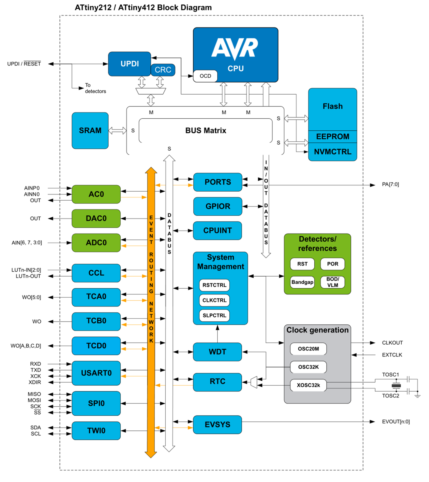
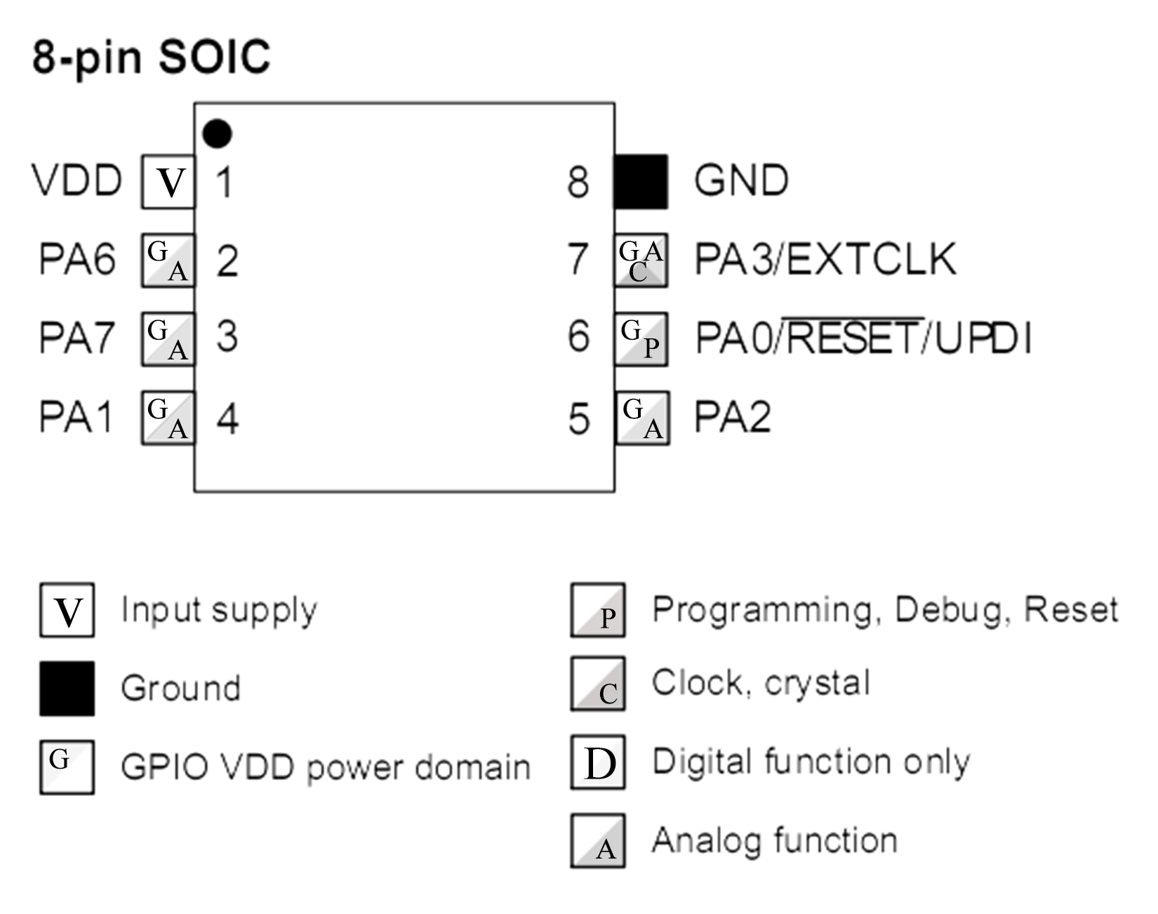
This series of ATtiny MCUs can run up to 20 MHz, with up to 4 KB of Flash ROM and 256 bytes of SRAM, as well as up to 128 bytes of EEPROM, all in an 8-pin package. Despite its small size, it has a large number of peripherals, which can be routed to any supported pin:
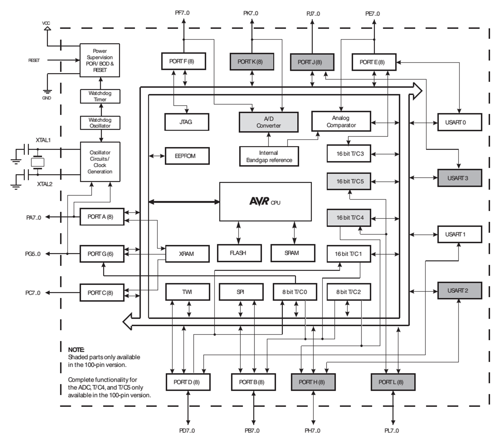
Contrast this with the popular ATmega2560 and related MCUs, which have the following properties:
|
Device |
Flash (KB) |
EEPROM (KB) |
RAM (KB) |
General purpose I/O pins |
16-bit PWM channels |
UART |
ADC channels |
|
ATmega640 |
64 |
4 |
8 |
86 |
12 |
4 |
16 |
|
ATmega1280 |
128 |
4 |
8 |
86 |
12 |
4 |
16 |
|
ATmega1281 |
128 |
4 |
8 |
54 |
6 |
2 |
8 |
|
ATmega2560 |
256 |
4 |
8 |
86 |
12 |
4 |
16 |
|
ATmega2561 |
256 |
4 |
8 |
54 |
6 |
2 |
8 |
With GPIO pins numbering in the dozens, the block diagram is correspondingly more complex, with many more port blocks for the I/O pins:
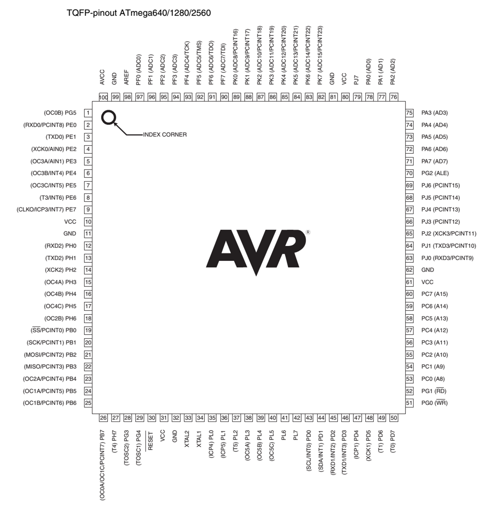
Here, all the incoming and outgoing arrows indicate a single pin or block of pins, most of them general-purpose. Because of the large number of pins, it is no longer practical to use an inline package format (DIP, SOIC, and so on) for the physical chip.
For the ATmega640, 1280 and 2560, a 100-pin TQFP package is used, here with the functionality of each pin indicated as found in its datasheet:
The ATxmega family is very similar to the ATmega, with a similar pinout, mostly differentiating themselves using architectural changes and optimizations, more ROM and RAM, and peripheral options.
Whether to pick an ATtiny, ATmega, or ATxmega MCU depends first and foremost on the requirements you have for your project, specifically the required input and output, types of peripherals (serial, SPI, I2C, CAN, and so on), and the size of both the code and the RAM required to run this code.