1
Basic Definitions
In order to describe communication between components and electronic subunits, first we must cover general notions such as the direction of communication and connection topology, as well as the concepts of exchange synchronization and information coding, finishing off with the concept of a protocol, which defines the rules that have to be followed. A protocol also defines access arbitration and cycles.
1.1. General points regarding communication
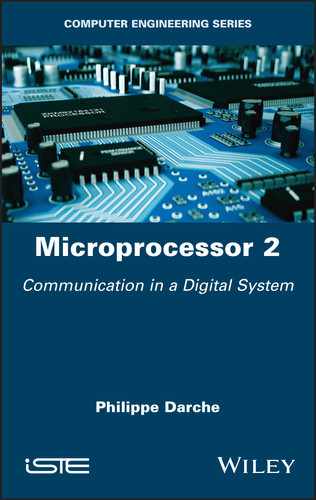
The direction of communication between two systems (Figure 1.1) can either be one-way (simplex) or bidirectional, and this can be either a full-duplex or alternating (half-duplex). Note here that the communication protocol (i.e. the link layer) cannot provide more than what the physical layer permits.
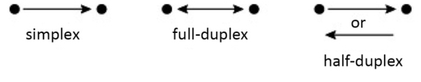
Figure 1.1. Direction of transmission
The entity from which the communication originates and which is generating the address and control signals is called the Master (M) or Initiator (I), and is represented by a square in Figure 1.2. The entity that replies and follows the commands is traditionally called the Slave (S), or Target (T), and this is represented by a square in the figure. If the bus can only take a single master, it is referred to as a single master system. If it can take several it is called a multi-master system (cf. § 2.2.5). If the medium is shared during emission, there can be a conflict of access to the resource (i.e. the bus or slave unit); this is called a collision. The collision can be either logical or physical. A physical collision can result in material damage if the electronic output stage is not designed for it. For this reason, access arbitration is needed (cf. § 1.6).
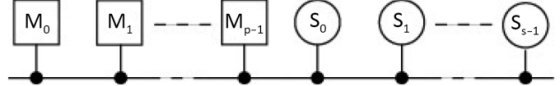
Figure 1.2. Model of a multi-master bus
To access the bus, each entity requires an interface called I/F (Figure 1.3).

Figure 1.3. Shared bus
In a one-way bus (simplex transmission), an emitter Tx can emit towards one or several receivers Rx. This is a divergent bus, which can broadcast information (Figure 3.16, for example, and cf. § 2.2). Another case that must be considered is where several emitters can only communicate towards a single receiver. This is a convergent bus that allows for the broadcall of information (cf. § 2.2). The existence of several masters can result in an issue of contention when multiple access requests are made to the communication carrier. The bus can be bidirectional (Figure 3.14, for example), with simultaneous transmission (full-duplex), or alternating transmission (half-duplex).
There are several topological variations, including the MUX-based bus (multiplex) and the AND–OR structure. Both are preferred to the SoC (System on (a) Chip). They are shown in Figure 4.28(a) and (b) respectively.
Since there are three main types of information (address, data and control) to be passed around the nodes of a bus in a microprocessor system, there are several ways for them to be transported: there are three combinations with one element, three combinations with two and one with three possibilities. These combinations specialize the bus, resulting in address buses, data buses, control buses, address– control buses, address–data buses, control–data buses and address–control–data buses (only one bus!). During an exchange of several types of information between two entities, for example, between an address and a piece of data, the transfer can make use of separate media (non-multiplexed bus), or they can use the same medium (multiplexed bus). The choice to multiplex is often one of cost: a bus takes up physical space on the Printed Circuit Board (PCB), which is expensive. The number of output connection points for each electronic component and even for the connectors must be taken into account, as the cost of an Integrated Circuit (IC) or a connector is directly linked to this amount. The first approach is better in terms of bitrate, as the buses are separate, with one for each information type. Time-division multiplexing1 is a solution that allows several different types of information to travel through the same bus, but at different times. The initial philosophy at Intel was that of multiplexing the address and data buses. An example is the 8088 microprocessor made by Intel for the IBM PC (Personal Computer, cf. § V5-3.2.1). This was in contrast to Motorola, which did not multiplex its address and data buses. Another example is the PCI (Peripheral Component Interconnect, cf. § 4.2.4). It should be noted that the information required for the transaction does not need to be presented all at the same time. For example, the information to be written can be presented after the address (“late write”, cf. § 4.4.1 in Darche (2012)). The flipside of multiplexing is that the information transfer time is usually longer as the information has to be (de)multiplexed before it can be accessed, resulting in delays in propagation. This can be done either through a process that is external to the communicating elements, or internally, and thus transparently. In the former option, the peripheral circuits communicate specifically with a microprocessor, usually belonging to the same commercial family, for example, the MPU (MicroProcessor Unit, µP for short) 8085 from Intel and its parallel interface circuit 8155, where the former’s (de)multiplexers were integrated into the latter. In the case of a bus with different pieces of information spread over different moments in time, multiplexing does not slow down the exchanges and therefore cannot reduce the bitrate.
1.2. Main characteristics
A shared bus is a common interconnection pathway between all of the connected nodes. It is made of a set of lines or communication channels along which the information flows. Usually, only signals are counted, as the power and grounding lines are contained in a separate power bus (cf. § 4.2.10). This number does not take into account electrical characteristics, for example, whether the signal is differential or not (cf. § 3.6.3 in Darche (2012)). At least three2 elements or nodes can connect to it; otherwise, it would be a point-to-point connection, also known as a link. These elements can be electronic components, electronic boards, peripherals or computer systems, depending on the level of observation. These buses can also be inside computer systems, particularly in a microprocessor (cf. § 4.2.9). Information is considered in a broad sense in this work, so it can refer to data, an address3, a command, a control, a state or even an interrupt request or its vector (cf. § V4-5.7). These lines are usually permanently grouped by information type or by function. The result is referred to as a dedicated bus. Two examples are the address bus and the memory channel (cf. § 7.2 in Darche (2012)). Thurber et al. (1972) define these buses as functionally dedicated4. A dedicated bus is more expensive in terms of connectors and electronics, but its interface is simpler in terms of design (no (de)multiplexing, for example). Otherwise it is undedicated. As the technology used is electric or electronic, the bus takes the form of electric conductors (electric ribbon cables, metallic traces in a printed or integrated circuit) through which the electric signals travel, most of the time in two states. Optics is a possible future development, but it remains currently under research (cf., for example, Feldman et al. (1999)). Fiber optics are used extensively throughout networks, however.
A bus can be of a unique design, produced by computer or microprocessor makers, or a regulated solution that follows established standards, coming from private solutions, or not. A standardized solution, which by definition provides generic characteristics, is usually less effective than an ad hoc solution, but it is usually cheaper due to the standardization of its components and systems (Commercial Off-The-Shelf (COTS) solution). In particular, defining a standard for the interface helps with design as it allows for interoperability and reuse of the modules.
A bus is characterized mainly by its width w (w bit-wide), its bitrate (incorrectly referred to as its transfer speed) and by its communication protocol that defines its signals. The typical values of w are 1, 4, 8 and multiples thereof, usually of eight. This is particularly true for data buses, as the data that passes through them are themselves multiples of eight5. The address bus, however, can also be expressed in other multiples, for example, the 8086 microprocessor from Intel whose address bus has a width of 20 bits. The width of the address bus gives the addressing capacity C = 2w memory words of the component that generated the address, which is usually the microprocessor. It therefore defines its Address Space (AS, cf. § V3-2.1.1.1). It represents the amount of physical memory accessible without any additional mechanisms, such as Virtual Memory (VM, cf. V2 on semiconductor memory). The width of address buses and data buses do not have to correlate with each other. Some examples are: (m/n) 16/8 (8-bit generation microprocessor), 16/16 and 21/16 (first-generation 16-bit microprocessor), 24/32 and 32/32 (32-bit generation microprocessor), etc. The width of the data bus is linked to the flow of information (cf. below).
A serial bus has a single communication channel (w = 1). A parallel bus has w channels (w > 1). In the first case, this means that only a single bit is sent at a time. In order to send a piece of data in the format n > 1, serialization must first take place, with the inverse operation, deserialization, taking place upon reception of the data (Figure 1.4). The number of signals is therefore low, which reduces the connection cost (cables, surface area and therefore number of PCB traces, connectors6 and number of IC package pins). There is no time delay between signals from different lines. Moreover, scalability, that is, increasing the bitrate, is made easier as all that is required is to increase the number of links. Serial communication is used in linked connections, mainly in Input/Output (I/O) interfaces. It can also be used in a bus, for example, in the coaxial cable Ethernet network IEEE 802.3™-2008 10Base2 and 10Base5 (IEEE 2008). There is a disadvantage in terms of bandwidth as service bits must be used in order to synchronize the exchange (start and stop bits of the interface RS-232 (RS for Recommended Standard), for example, cf. § 8.2.2 in Darche (2003)) and to detect and possibly correct transmission errors. Moreover, (de)serialization takes time. Each communicating element has a (de)serializer that either includes or rebuilds the clock signal, depending on the case. This is the SerDes (Serializer/Deserializer) technology. The SPMT™ (Serial Port Memory Technology) uses this technology (cf. § 3.6.8 in Darche (2012)). SerDes type transfers usually utilize an 8b/10b encoding (Widmer and Franaszek 1983), which is 8 bits of information encoded into 10 bits in order to eliminate the Direct Current (DC) of the signal (DC-balanced) so that the clock signal can be rebuilt. The useful bitrate is then equal to 80% of the raw bitrate.

Figure 1.4. (De)serialization operations in the serial link
In parallel transmission, n (n > 1) bits are sent to an exchange when the format of the data n is equal to that of the interface (Figure 1.5). The word to be transmitted can have a higher format, for example k × n bits, k ∈ ℕ∗. Parallel transmission will then take place in subwords of n bits. In this case, it is called subword-parallel transmission.

Figure 1.5. Format n parallel link
In that last case and in the case of serial transmission, there is the issue of the order in which bits and bytes are sent. This is the problem of Little Endian (LE) and Big Endian (BE), identified by Cohen (1981) (cf. § 2.6.2 in Darche (2012) and § V1-2.2.1). James (1990) explored this problem looking at the bus specifically. Note that the byte swapping function, as present either as a microprocessor instructions (bswap, for example, cf. § V4-2.6.1), or implemented in bus interface circuits (a bridge, for example) or in communication circuits or controllers (cf. Sriti (1999), for example) allows for this order to be reversed. Moreover, for the last mode, there can be an issue with the alignment (cf. § 2.6.1 in Darche (2012)), meaning that a word in the format n is not transmitted in a single bus cycle, but rather over two cycles, as shown in the examples of Figure 1.6 for a transmission in the 32-bit format.

Figure 1.6. Possible misalignments during the transmission of a 32-bit word (Borrill and Theus 1984)
The disadvantages of serial transmission tend to be the advantages of parallel transmission, and vice versa. In absolute terms, parallel communication is n times faster than its counterpart (for k = 1) for a set clock rate. The bitrate can be increased simply by widening the bus. There is no (de)serialization time. The synchronization signals are additional signals, increasing its width correspondingly. There is therefore no overhead in terms of bitrate. However, the connection cost (cable, PCB and connector) is greater than for its counterpart as it takes up more space. Dealing with errors is also more complicated. The problem of clock skew between signals (line-to-line skew) has to be considered for high bitrates (cf. § 3.5.3 in Darche (2004) and § 3.6.6 and 7.1.2 in Darche (2012)). Progress in fast electronics means that nowadays the serial link is adequate for most bitrate requirements. Moreover, it is becoming widespread in computers, replacing buses with simpler point-to-point connections. The link is made up of a pair of one-directional channels of opposing directions. This is referred to as a link or lane, for example the PCI Express bus (PCI-E or PCIe), described in Jackson and Budruk (2012).
The flow of information is measured in number of bits, or multiples thereof (usually bytes), transmitted per unit of time. It is a function of the information format n. The base unit is the bit per second (bit/s, b/s or bps), and its multiples are powers of 10 (× 103 × k, k ∈ ℕ∗). In increasing order, there is the kilobit/s (kbit/s = 103 bit/s or kbps), the megabit/s (Mbit/s = 106 bit/s or Mbps), the gigabit/s (Gbit/s = 109 bit/s or Gbps) and the terabit/s (Tbit/s or 1012 bit/s or Tbps). These units7 are mostly used for networks. The bit per second is the equivalent to a baud for a valency of 2. For the bus and the interfaces, we can also use the byte per second (B/s) and multiples thereof, such as the kilobyte/s (kB/s = 103 bytes/s), the megabyte/s (MB/s = 106 bytes/s), the gigabyte/s (GB/s = 109 bytes/s) and the terabyte/s (TB/s = 1012 bytes/s). A dedicated bus provides a higher bitrate than its generic alternative, and handling the electronics is simpler, especially for the controller and interface electronics. It is more costly in terms of connections, however.
A distinction must be made between two types of rate: the raw bitrate or data rate, and the useful rate or throughput. The data rate is the maximum rate that the bus is able to physically handle. It is tied to the bandwidth and to the Signal-to-Noise Ratio (SNR, which is equal to 10 log10(Ps/Pn) in dB) (Shannon 1948). The throughput is the mean rate that the user, usually a processor or a memory controller, will be able to make use of. It is calculated as a function of the channel’s bandwidth, the format n of the information and the encoding used. From this, the rate relating to handling the data rate communication is subtracted. We can thus define the efficiency of a bus η as the ratio of the number of useful bits to the total bits in the message. There is also the burst transfer rate (cf. § 2.2). Moreover, there can also be transfer modes like the Double Data Rate (DDR) or Quad Data Rate (QDR), as there is for Random Access Memory (RAM, cf. § 4.6.2 and 6.5 in Darche (2012)), where each edge of the transmission clock transmits one piece of information, thus theoretically doubling, or respectively quadrupling, the data rate.
A bus is said to be passive if it contains no active electronic components (i.e. transistors or diodes). It simply ensures the connection between elements of the bus. Figure 1.7 gives two examples of this. From left to right, it shows an I/O bus unit with Hard Disk Drives (HDD), by Integrated Drive Electronics (Schmidt 1995) in the form of a flat cable and of a backplane bus (cf. § 4.2.7). An example of this last item was bus S-1008, standardized under reference ANSI/IEEE Std 696-1983 (ANSI/IEEE 1982b). Otherwise, it is said to be active. The driver is tasked with amplifying the signals and controlling the bus. Other technologies that can be utilized are radiofrequencies, infrared or even lighting technologies (laser). These are limited to wireless connections. Optics is a possible next step for buses, but this is still in the research phase, although they are starting to be used in the extension bus and the I/O bus. Savage (2002) develops this approach further. A major obstacle is cost and the need to convert optical/electrical signals.
A bus is said to be external when it is located outside the computer. This is nearly always an I/O bus (cf. § 4.2.6). Otherwise, it is internal. The SCSI (Small Computer System Interface) I/O bus could be both internal and external. Internally, it linked the mass storage units. Externally, it could exist as part of peripherals such as a printer or a scanner (cf. respectively § 6.3 and 5.3.1 in Darche (2003)).
Figure 1.7. Ribbon-cable I/O bus (IDE) and a backplane bus. For a color version of this figure, see www.iste.co.uk/darche/microprocessor2.zip
Bus mechanics relate to all aspects of the assembly of components and printed circuits, as well as all aspects of connection. Bus mechanics specify, among other things, the maximum length of the bus, specifications of the connector/s and, potentially, the size and fixation type of the electronic card (motherboard, daughterboard or expansion card) and of the housing, cabinet or rack that houses them. The connector specifications state their maximum number, size, position, distance between two connectors, and their interconnection gap, etc. The connectors of an expansion bus, if installed onto a printed circuit like in the motherboard of a micro-computer, take up a significant amount of space (1/4th to 1/3rd of the surface area of a personal computer (PC)-type motherboard) and therefore contribute significantly to the overall cost of the system. A bus’s connections should not be underestimated as they are without a doubt its weakest link and make it less reliable.
Electrical characteristics relate to the voltages and currents of input, output and I/O, and the minimum, maximum and nominal voltages and currents of the signals (cf. § 1.2 and 2.2.1 in Darche (2004)) and of the bus lines. They are primarily those of the logic used (cf. Chapter 2 in Darche (2004)). The electrical load, as seen by the emitter, is an important parameter as it directly affects the rise and fall times of the signals. They rely on the bus itself, as well as on the connector, the daughterboard and possibly any stub relaying the bus towards the connector. This load is variable and depends upon, among other things, the number of nodes and whether all the slots are occupied by an inserted electronic card, thus forming a load. Moreover, each connector makes the bus longer by creating a stub that derives the main bus, or “backbone” (Figure 1.8), thus modifying the electrical and temporal characteristics of the bus. This load is complex (mathematically speaking) as it contains resistive, capacitive and inductive components respectively. This derivation can also introduce impedance mismatch, which is a potential source of electrical disturbance due to the reflection of signals at the end of the line. This characteristic should be considered when determining the maximum number of connectable elements.
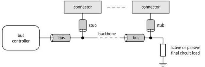
Figure 1.8. Bus lines and derivation stubs
The bus also possesses temporal characteristics that are tied to the protocol or to the technology used, such as the rise, fall and propagation times of the signals, and the temporal relations that exist between them. The bus-settling time is the time required for the signal to become stable. Another important time is the flight time tflight (cf. § 3.3.4 in Darche (2012), with an example in Intel 97). It is the time taken by a signal to cover the full length of the bus. It takes into consideration all of the propagation times of the interface electronics, any skews and the time window of capture by the receiver. It also includes the bus propagation time tL (cf. § 3.3.1). One empirical rule is that 6 × tflight should be less than 30% of the Unit Interval (UI, or in other words a period of 1 bit) of the eye diagram (or eye pattern, cf. § 3.5.3 in Darche (2004) and § 7.1.2 in Darche (2012)) for a stable state at the sampling point at 50%. The protocol also includes delays such as those linked to arbitration.
A bus is poorly scalable, in that the addition of nodes has a negative impact on its electrical and temporal characteristics, limiting it practically. The access time and rate are worsened by distortion and the arbitration time, and the designer must plan for the worst case, which is not very efficient.
SUMMARY.– The advantages of a bus are its versatility and adaptability. New electronic cards can be added to it easily. Cards can be transferred from one computer to another as long as they have the same bus standard and maintenance can be ensured. The computer system itself can be designed to be partitioned. It is relatively inexpensive as it constitutes a primary approach rather than a collection of shared cables or traces. The main disadvantage is that it forms a bottleneck (or tailback) in terms of communication. The bandwidth of a bus limits the I/O data-rate. Other characteristics also limit this rate, such as the length of the bus, as well as the number of nodes. Furthermore, if the nodes are heterogeneous, characteristics such as latency or data transfer speed will be heterogeneous too. Scaling up is just as hard, and can even prove to be impossible.
1.3. Synchronism and asynchrony
Those involved in an exchange must communicate at speeds that are compatible with this exchange. An exchange can be synchronous or asynchronous, depending on whether a clock signal pacing the transfer is explicitly sent or not9. In a synchronous bus (with an interconnection), a master clock10 provides a clock signal that paces and synchronizes the exchanges between elements of the bus. This signal is distributed between all of the nodes of the bus, and is either amplified (radial clock distribution, Figure 1.9(a)) or not (bussed clock distribution, Figure 1.9(b)), with each node able to generate a local clock. The problems associated with the clock are temporal in nature (e.g. skew, jitter, noise, etc.), but can also be electrical, such as metastability, for example, the criticality of which is directly proportional to the frequency. Moreover, the user module (cf. § 3.1) can either use this signal or have its own clocks.

Figure 1.9. Distribution of the (a) radial or (b) bussed clock signal
Each operation has to be carried out within a constant time interval that is tied to its period. Otherwise, a transfer error takes place. In nearly all cases, the signal in a bus is handled by the edge of an active clock (this is an edge-triggered logic model), marking the start of an exchange. However, a level-sensitive logic model can also be considered. Figure 1.10 shows the causal link between signals, with an example of an exchange request with a read receipt provided. In the purely synchronous model, no cycle start signal is needed as it is the active clock edge that marks this start. The time characteristics are fixed. The period of the clock signal must therefore be greater than the propagation time of the bus plus any times relating to the logic, such as the setup time tsetup.
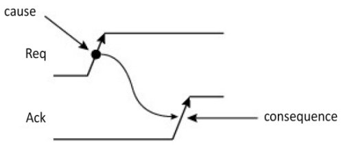
Figure 1.10. Causal link between signals
The cadencing diagrams are asynchronous or synchronous, classical or derived, mesochronous11 or plesiochronous. In a mesochronous system, local clocks are derived from a global clock. Delays in the transfer of clock signals are not even, resulting in phase shifts. A mesochronous system is said to be “static” when the phase difference between clock signals of the same frequency does not vary during system operation. A “dynamic mesochronous system” exists when this phase difference varies for each component, for example, because of temperature or supply voltage variations. An example of such a system is the basic Rambus channel (cf. § 7.2.1 in Darche (2012)). If the clocks are independent and not synchronized but the average frequency is the same, so with a slight drift, the communication is said to be “plesiochronous12”. An example is the RS-232 series interface (cf. § 8.2.2 in Darche (2003)). When the frequencies are different, the communication is said to be “heterochronous13”. More details on synchronization can be found in Messerschmitt (1990).
Designing a synchronous system is harder than designing an asynchronous one. The clock domains and of their interactions must be taken into account (Clock Domain Crossing, CDC). The problem has been covered in sections § 3.6.6 and 7.1.2 of Darche (2012). A purely synchronous system carries out one transaction per clock period. This is called a bus cycle. This is not the case in a semi-synchronous system (also called pseudo-synchronous or clocked), which is instead characterized by a longer time interval, the bus cycle of which is a multiple of the system clock period. This number of periods can be fixed, limited or free. During a transaction, transmission can become asynchronous through the help of a wait request signal (the Wait signal, for example), adding clock cycles in order to lengthen the transaction. An example of a semi-synchronous bus is the NuBus (TI 1983). A variation of this is source-synchronous clocking (cf. § 7.1.2 in Darche (2012)). An example of a synchronous bus is the Multibus II backplane bus from the company Intel, standardized through the reference ANSI/IEEE Std 1296 (IEEE 1988).
The asynchronous bus represents a different approach, the advantage of which is that a global clock signal is not used, which can be limiting in terms of design time. The dedicated time slot can be made longer as needed. Thus, exchange times can be adapted to the speed of the nodes. However, there is a risk of blocking the exchange if there is no limit to the response time, as a new cycle cannot begin if the previous one has not finished. This means that the bus can remain indefinitely allocated to the master that holds it. Two examples of asynchronous buses are the Unibus™ backplane bus from the company Digital Equipment Corporation (DEC) and the Multibus I from Intel, standardized through reference ANSI/IEEE Std 796 (ANSI/IEEE 1982a).
In terms of asynchronous protocols, the first group is those with one-way control, that is, controlled by a single component of the exchange. This is referred to as a “One-Way Command”, or OWC. It is simple, with a single Req(uest) (the forward signal). Figure 1.11 highlights this through the reading of a piece of information. The request signal is activated (timestamp 1). Next is the positioning of the information by the source S after a certain amount of access time ta (timestamp 2). When the request is deactivated (timestamp 3), the information is removed by the slave source S (timestamp 4). The temporal characteristics of the bus, in particular the propagation delay tpd, must be considered in order to quantify the access time ta. In this version, the transfer time is adapted to the requester as it is the latter that (de)activates the request signal (“destination-controlled transfer”). The main disadvantage is that there is no check for the validity of the exchange by the destination D. If the source fails, it cannot carry it out. Note that time tdis (dis for disable) qualifies the deactivation time of the three-state electronic buffers (cf. § 3.3.4)
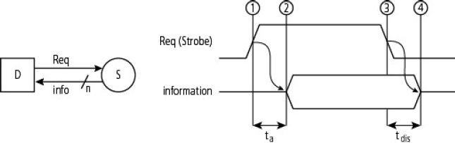
Figure 1.11. One-way control protocol
Another term used to refer to one-way control is “strobe protocol”, as shown in Figure 1.12, which highlights the transmission of a piece of data (source-controlled transfer). After a certain data setup time tsetup (timestamp 1), the emitter signals its presence (timestamp 2) and its retreat (timestamp 3), which becomes effective during step 4. The limits of this protocol are seen again in the transmission of a data item when there is a transfer error if the receiver is not listening or does not account for it sufficiently quickly.

Figure 1.12. Strobe protocol
The handshake protocol was created as a solution to the downsides of the strobe protocol. It is the most common protocol among unclocked systems (also known as clockless, or self-timed systems), and is source-controlled. In a master/slave setup, a master M sends a request to the slave S, which must answer. It uses two signals, which are a Req(uest) and an Ack(nowledgment). The former is used as part of the signaling, while the latter is a backward signal. As there are two signals, the protocol is said to be one of double-track handshake signaling. These signals can be asserted or non-asserted. A Comp(letion) signal marks the end of processing. Depending on the presence and direction(s) of the transmission of information (Figure 1.13), the signal can exist in one of two versions, with either two or four phases, and with four different channels, which are nonput, push, pull and biput The nonput channel (a) does not exchange data, but rather allows for synchronization between the communicating elements. The push channel (b) sends data, while the pull channel (c) receives it. The biput channel (d) is bidirectional. The black dot in the figure means that the entity is active in terms of communication, while a hollow dot means that it is passive. A functioning module can be integrated into the channel as an element of combinational logic – the whole forms a stage of the pipeline (cf. § 4.5.1 and 6.1 in Darche (2012) and V2 on future microprocessors).
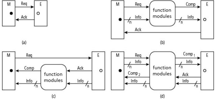
Figure 1.13. The four possible channels of the handshake protocol
There are three different versions of this protocol depending on the position of the synchronization signals: non-interlocked, half-interlocked and complete. Complete interlocking means that no more exchanges can take place as long as the previous one is not yet finished and signaled. In the two-phase handshaking version, shown in Figure 1.1.4, there are two types of exchange, which are the “up” handshake, which uses the Req↑ and Ack↑ signals, and the “down” handshake, which uses signals Req↓ and Ack↓. For each of them, there are two transitions, or phases, embodied by the edges of the request signal Req and the receipt acknowledgment signal Ack. The level of the signals is therefore irrelevant, as opposed to the rising or falling edges (this is “edge-sensitive” control, or transition signaling), which are significant (it is an “event-based” protocol), hence the term “two-stroke” signaling (or two-cycle signaling, transition, Non-Return-(to-)Zero (NRZ)). At the end of the exchange, these two signals are in the same state, whereas during the exchange, they were in opposite states. There is an initialization state, which is the transition of the reception signal, here Ack↓, which sets off the exchange (dashed line). Note that the acknowledgment signal can be complemented.

Figure 1.14. Rising and falling versions of the two-phase handshake protocol
In the case of a push channel (Figure 1.15), once the information has been positioned, a request is sent out in the form of a transition of request signal Req. When the receiver has processed the information, it signals for it through a transition of the acknowledgment signal Ack.
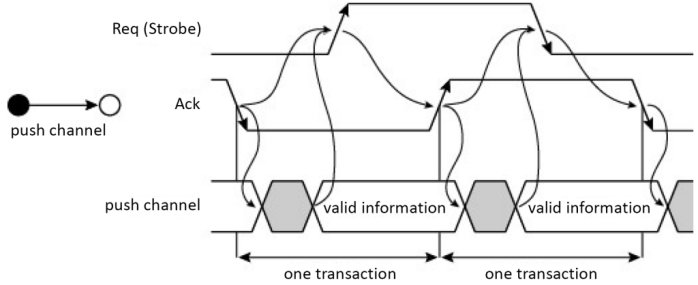
Figure 1.15. Two-phase handshake in a push channel
In the case of a pull channel (Figure 1.16), the request leads to the information being positioned by the source, which then signals for it through an acknowledgment.
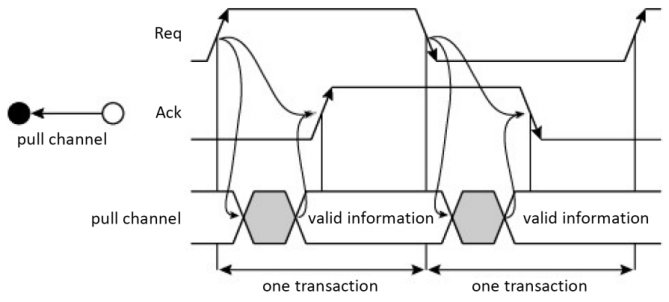
Figure 1.16. Two-phase handshake in a pull channel
Note that there is an overlapping of data validity between the two previous channel types during a transaction, as shown in the two gray vertical areas in Figure 1.17.
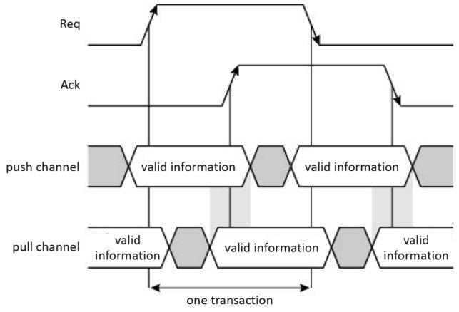
Figure 1.17. Validity overlapping between the two channels
In order to eliminate the toggle circuit during hardware implementation, a four-phase handshake protocol is required, also known as double-handshaking. Here, the level of the signals is significant (level-sensitive control). In the complete interlocking version shown in Figure 1.18, there are two types of exchange, which are the up handshake and the descendent handshake. For each of these, there are two transitions, or phases, which are embodied by the edges of the request signal Req and the acknowledgment signal Ack, hence the term four-stroke (or four-cycle) signaling. At the end of the exchange, these two signals return to their initial state 0, while during the two phases, they were in opposite states. For this reason, the double handshake is called “Return-(To-)Zero (R(T)Z)” signaling. An initial state is an equilibrium of the states of the protocol signals. The dashed line in Figure 1.18 represents an example of this.

Figure 1.18. Four-phase handshake protocol
For a push channel, the Req and Ack signals respectively mean valid data (Strobe) and a completion signal. As shown in Figure 1.19, the emitter signals the availability of the information through the rising edge of the strobe signal Req14 (Req↑). As previously, receipt of the positive edge of the acknowledgment signal Acq (Ack↑) results in the removal of the information and deactivation of the request signal (Req↓), in turn leading to the deactivation of the acknowledgment signal (Ack↓).

Figure 1.19. Four-phase handshake protocols for a push channel (Darche 2012)
There are actually four versions of this channel: (Figure 1.20) early (Furber and Day 1996; Furber and Liu 1996), broadish (or extended early), broad and late. For the first three, there is valid data on the rising edge of the Req request – it is therefore the invalidation of this data that differentiates them according to the three edge possibilities. The data is no longer valid on the rising edge of the acknowledgement signal for the early mode, on the falling edge of the request signal for the broadish mode, and on the falling edge of the acknowledgement signal for the broad and late modes. For the late mode, the data is valid on the falling edge of the request signal.

Figure 1.20. Four versions of the four-phase handshake protocol for a push channel
Figure 1.21 shows the “data request” version (pull channel), again with the four variations.
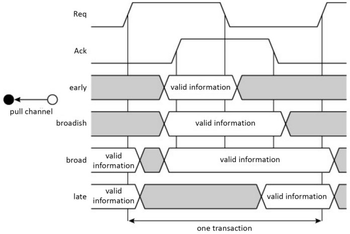
Figure 1.21. Four versions of the four-phase handshake protocol for a pull channel
Figure 1.22 shows the other two possible versions of the handshake protocol, which are “half-interblocked” and “non-interblocked”. The causality of the exchanged is indicated with arrows. The second version is pulse-based signaling, active on the edge or levels, a technique that is similar to transition-based signaling. The operating mode was studied by McCluskey (1962) and his asynchronous version is presented in Nyström and Martin (2002).

Figure 1.22. Half-interblocked (a) and non-interblocked (b) handshakes (Thurber et al. 1972)
Figure 1.23 shows how this can be applied through two examples, a read (a) and a write (b), both asynchronous, carried out by the CPU (Central Processing Unit). The R/#W (Read/#Write) signal is not shown so as to not overload the illustration.

Figure 1.23. Exchanges between CPU and the memory through a handshake
To summarize, the OWC and handshake protocols are used by the asynchronous and semi-synchronous buses. The two-phase handshake is quicker than the four-phase, and requires less current in CMOS logic (Complementary Metal Oxide Semiconductor, cf. § 2.4 in Darche (2004)). It is particularly well suited for slow communicating systems (Renaudin 2000). The two Req and Ack signals can alternatively be carried through a single cable. This approach was named single-track handshake signaling by Van Berkel and Bink (1996), and its study goes beyond the scope of this work.
1.4. Coding data
The validity of the transmitted data is inherent to the synchronous protocol, as data and validity are correlated. There are several solutions for carrying out validation in an asynchronous protocol. The first is called bundled data. The term comes from Sutherland (1989, 2007), and leads on to the notion of bundling constraint, which forces the data to accurately consider this constraint before proceeding to signaling. A done signal accompanies the transfer of information and validates the information. A superior solution to this is the use of protocol signals Req and Ack as well as the handshake. A single cable is used to transfer a bit of data, hence the notion of single-rail data encoding. For the coding to not be affected by the propagation delay, unlike in the first solution, the coding can be carried out in three or four states. This coding uses two cables (two rails) to encode the value of the validity of the data. This constitutes a robust end solution that is dependent on the data but requires an associated detection logic (cf. exercise E1.1). Three-state encoding is governed by the truth table shown in Table 1.1. It is called Dual-Rail (DR) data encoding. This type of approach can be generalized to n number of rails (Multi-Rail or MRn) while working in base n. For example, DR is MR2 encoding. Four-state encoding is governed by the same truth table shown in Table 1.1. The first bit gives the binary value and the second bit gives the logical parity (cf. § III.6.6 in Darche (2000)). We can also see that any change along the second rail marks a new bit. Note that the dual-rail code is also called 1-of-2 code, and is part of the 1-of-n codes, that is, the one-hot codes with a size of n, who themselves belong to the m-of-n code family.
Table 1.1. Interpretation of code words in three- and four-state dual-rail codes
| Code words (format n = 2) | States in a three-state dual-rail code | States in a four-state dual-rail code |
| 0 0 | Invalid or reset | 0 even |
| 0 1 | 0 | 0 uneven |
| 1 0 | 1 | 1 uneven |
| 1 1 | Not used | 1 even |
Another aspect of coding relates to the current consumption. Yand et al. (2004) suggests encoding the most frequent bit patterns that circulate around the data bus in order to reduce the current consumption of the electronic buffers. This approach was already suggested for solid-state memories with the bus invert by Stan and Burleson (1995), and is further explored in the second volume on future memory devices.
In the microprocessor, the instructions can also be encoded (cf. § V4-1.1.1).
1.5. Communication protocol
In order to exchange information, first a communication protocol must be defined that can manage this exchange. A protocol is a set of conditions and operations, whose order must be strictly respected for the transaction to take place. The rules to follow for the signals are physical specifications (electrical values) and time and causality constraints of the operations. The operations are the activation or non-activation (by level or by edge) of signals of state, control, and address and data positioning. When a master accesses a slave, it states the type of access, read or write of a word, read or write of a block (in a block transfer), Read–Modify–Write (RMW mode) or a word, writing after reading (write-after-read mode) or access in interruption mode (address-only and interrupt acknowledge cycles. RMW mode allows for synchronization and locking mechanisms to be implemented, such as the semaphore, or lower down, the test-and-set instruction (cf. § V4-2.6.1). The two main corresponding control signals (cf. § 3.2) are read enable or signalization signals (#R, #RE (E for Enable), #Rd or #RS (S for Signal)) and the same for write (#W, #WE, #Wr or #WS). There are also spatial characteristics that specify the information to be exchanged, and in the case of communication through bundles, the structure of the messages (especially the size). If communication is carried out through a datagram (i.e. a message), the protocol specifies its size (unit: bit or byte) and its structure, that is, the different fields (spatial characteristics), as well as the length and sequencing (temporal characteristics).
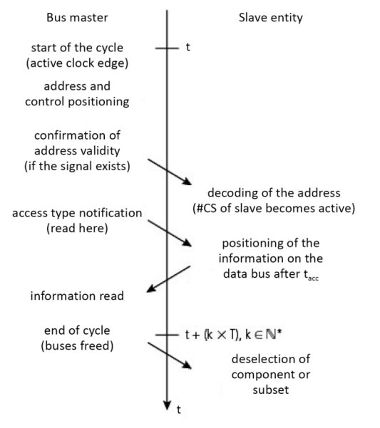
Figure 1.24. Sequencing diagram of a synchronous read
Figure 1.24 shows a synchronous operation, with a master, in this case, a processor, carrying out a read operation in a memory device. The arrow points to an action or cause that implies a new signal condition. The transfer is said to be addressed, as the correspondent is unique and chosen by the address. It sends the address along the address bus, which is subsequently taken into account by all of the address decoders (cf. § 2.2.2 in Darche (2003)) of the slave entities. The entity involved is accessed through activation of its selection signal (CS signal for Chip Select or CE for Chip Enable)) and send the desired data back. Remember that everything is synchronized to a clock and that the cycle has a duration of k × T, k ![]() , with T the period of the clock. The synchronous protocol is deterministic.
, with T the period of the clock. The synchronous protocol is deterministic.
It is possible to functionally split a cycle, referred to as a “transaction”. This term refers to a coherent unit during processing, which can be decomposed into an ordered sequence of unitary tasks. It is the logical activity unit of the bus or bus cycle that takes the form of a sequence of signals. This sequence follows rule flows that are gathered together in a communication protocol. If a clock synchronizes the operation of a bus, then the transaction takes places during one (in the case of a synchronous bus), or several bus cycles (in the case of a semi- or pseudo-synchronous bus). Only in the case of a multi-master environment does the clock start with an access request, followed by an arbitration phase (also called selection phase) between those requesting access to the bus. Once this arbitration phase is over, the chosen one then engages in the exchange, which is divided into an addressing phase, an information transfer phase (Figure 1.25) or even, in more complex protocols, an error detection and signaling operation phase.

Figure 1.25. A bus transaction
There are four fundamental pieces of information that must pass through the bus: the addresses of the source and of the destination, the information being transported and the operation that is to be executed. Usually, the source address is implicit. The information to be transferred is typically a machine instruction, data or an address, but it can also be a command, control, state or an interruption request or associated vector, etc. Note also that the addressing phase can be prolonged during the transfer phase, thus blocking the address bus, most likely unnecessarily. The issue can be addressed by transforming the read operation into a write operation for the case of a transfer between I/O controllers, or between the bus bridge, as proposed by Okazawa et al. (1998). The operation to be executed is a read, a write or a read–modify–write, but there are also special cycles (cf. § 2.2). In terms of the slave, the phases of access request, address decoding and transfer will take place in succession. A bus initialization phase is potentially required in order to power on the calculator or on demand. This involves ordering the powering on or off of the modules, in a set order if required, and to place them in a known state.
We can now establish the chronogram presented in Figure 1.26, which relates to the exchange as seen by the microprocessor. The access time tACC is the minimum time needed before the data can be processed. tDSR is the data setup time that takes place before the microprocessor can begin processing. Note that there is a data hold time at the end of each cycle, tDHR or tDHW depending on the operation, and tAH for the address. A synchronous transfer is faster. It makes design easier (simple logic) and guarantees exchange times. However, for this to happen, all elements of the bus have to work at the same frequency. The main principle of synchronous communication is strict adherence to the times, without which there is a risk of transfer errors. The cycle length tcyc, in particular, is fixed.

Figure 1.26. Simplified chronograms of synchronous read and write operations in the MC6802 microprocessor
Figure 1.27 gives an example of read access for a microprocessor using a multiplexed address/data bus. The ALE signal (Address Latch Enable) signals the presence of a valid address on the bus. The exchange type is “relaxed synchronous” as the cycle is prolonged by several reference clock periods, depending on the state of the Ready signal. In this synchronous version, the length a memory access time is measured in bus cycles, with one bus cycle being made of a number of clock cycles. More generally, the number of cycles depends on the length m of the data bus, the format n of the information and whether the access or information is aligned or not.
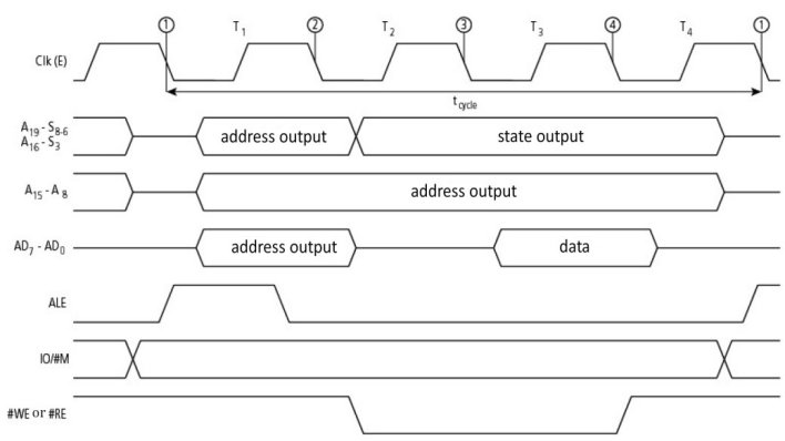
Figure 1.27. Read cycle with address/data multiplexing (iAPX88 microprocessor from Intel)
The alternative is an asynchronous operation. This has the advantages of reduced current consumption, which is vital in mobile systems, and greater flexibility in terms of design. However, there is no time guarantee, and specific transfer protocols, based on handshaking (cf. § 1.3), for example, must be established. Figure 1.28 shows a four-phase handshake.
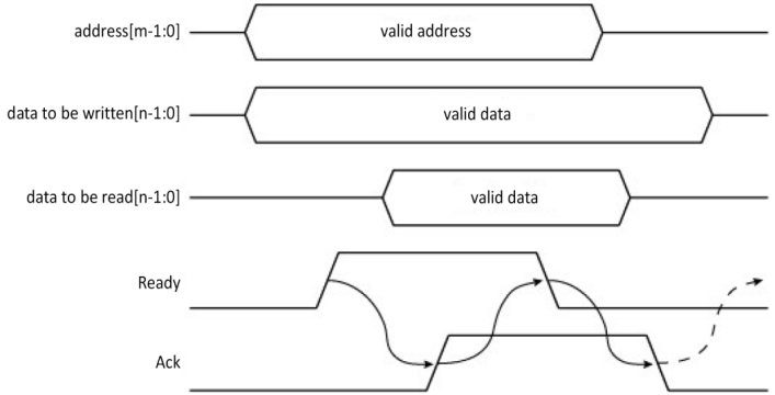
Figure 1.28. Read or write cycle with a four-phase handshake
The first one uses two signals, a strobe signal (Ready, in this case) and an acknowledgment signal, which enables a feedback signal. The transaction requires the bus to be crossed twice, thus slowing the exchange, as this is one more than in the synchronous version. During an asynchronous operation, the beginning of the protocol is the same as previously described, except that the reading of the data is tied to an acknowledgment signal from the slave (e.g. the -DTAck signal from the MPU MC68000 by Motorola). It is possible for the signal to not arrive, thus blocking the exchange, and consequently the bus (Figure 1.29). Mechanisms like the watchdog (cf. § V3-5.3 and § 3.3.1 in Darche (2003)) can unblock this situation, generating a bus error in the form of a Negative Acknowledgment (NK), through a third-party component, for example. A lack of addressable components can easily be detected, as it is given away by the lack of response.
The advantage of asynchronous communication is the ability to mix slow elements with faster ones on the same bus without any specific adaptations. The fast elements adapt to the speed of the others (“leveling down”).
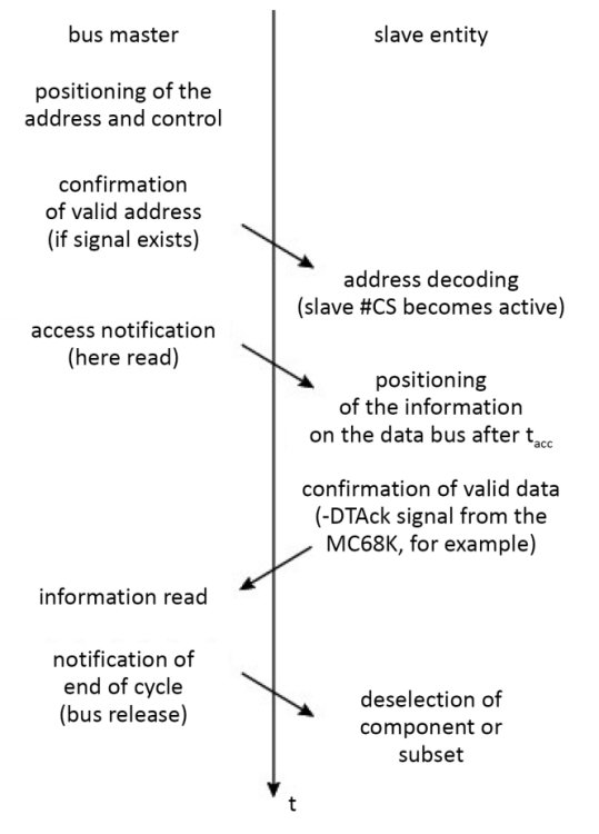
Figure 1.29. Diagram of an asynchronous read sequence
Figure 1.30 presents a completely asynchronous read by the MC68000 microprocessor. Once the address has been positioned, the #AS (Address Strobe) signal marks the start of the bus cycle. The read/write (R/W) signal is activated for one read. The slave activates the #DTAck signal in order to tell the MPU that the data to be read has been positioned on the bus. The #UDS/#LDS (Upper/Lower Data Strobe) signals let us choose the format of the operation. In these chronograms, we can recognize a handshake with interblocking (cf. 1.3), where the Req/Ack signals are represented by #AS/#DTAck, which are active in the low state. A more complete version can be found in Figure V3-2.20.

Figure 1.30. Asynchronous read cycle in the MC68000 microprocessor
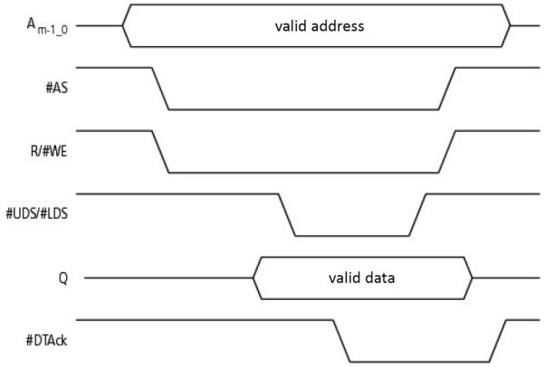
Figure 1.31. Asynchronous write cycle in the MC68000 microprocessor
An asynchronous write cycle (Figure 1.31) starts, as previously, with the activation of the #AS and write signals. The data is positioned by the CPU, which signals by activating the #UDS/#LDS signals, which mark its validity. A more complete version of this is the one shown in Figure V3-2.20.
An example of a semi-synchronous transfer is the one presented in Figure 1.32, which shows a memory access through a “transputer”, a microprocessor from the company Inmos Ltd (taken over by STMicroelectronics). One read cycle normally takes place over six half-periods; here, it is made longer by adding a half-period of waiting W, as sampling of the state of the delay signal is done on the falling clock edge, before the end of cycle T4. The events are discretized here. The number of half-periods added is limited physically.
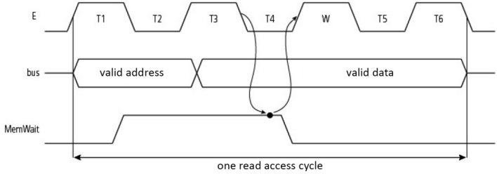
Figure 1.32. Simplified chronograms of an asynchronous read by transputer
Other variations of cycle lengthening can be considered. One example is shown in Figure 1.33 where the wait request signal must remain active for the amount of time needed for propagation. The time is here said to be continuous, as there is no clock signal interfering. The Wait signal allows the exchange to be lengthened.
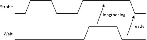
Figure 1.33. Lengthening a cycle with the handshake (from Nicoud (1987))
Another variation, still of the “handshake” type, is presented in Figure 1.34. It is run in 32-bit microprocessors, where a positive acknowledgment ends the exchange. In the case where the slave cannot satisfy the request, a negative acknowledgment
NAck is sent. In this way, the handshake is able to carry out flow control. It is said to be bounded.

Figure 1.34. Lengthening a cycle with positive and negative acknowledgments (from Nicoud (1987))
An addressed selection involves providing an address or a range of addresses to a slave. An addressed transfer involves providing an address which will then be decoded in order to select (i.e. activate) a slave. Typically, the slave has defined addresses. One variation is geographical addressing, which tells us which card is currently occupying a given slot. For this, each slot is attributed a number, called a slot space, and each connector is given an equal addressing zone. The most significant bits (MSbs) of the address are used to identify the location. Both the NuBus and VME (Versa Module European) buses, to only name a couple, use this type of addressing. Such an approach simplifies design by splitting the addressing space by number of connectors.
Borrill (1988) provides another approach to classing protocols than the standard synchronous–asynchronous dichotomy. He suggests three criteria, which are localization of the information validation (the locus), periodicity and flow control. The locus determines who has responsibility for the validation, whether it is the source (source-controlled), the destination (destination-controlled) or whether it is centralized. The periodicity states whether the exchange is periodic (fixed frequency) or aperiodic (variable frequency or synchronization). The control flow can be bounded (handshake) or not. On top of this, we can add the arbitration characteristics (cf. the following section).
1.6. Access arbitration
When there are simultaneously different access requests made to a bus, interruption requests (cf. Chapter V4-5), or Direct Memory Access (DMA, cf. § 2.2.2) requests made by a master or a slave (only for the first two), access arbitration to the bus is necessary. This involves choosing a master among n and allowing it to take the bus (grant). Access to the resource is exclusive. The electronics of the bus must be adapted in terms of output stages in order to (dis)connect to the arbiter request in a three-state logic, either open-collector or open-drain logic, or open-emitter or open source logic, depending on the technology used (cf. § 2.2.1 and 2.3 in Darche (2004)). In the case of a bidirectional bus, the direction of the flow of information must be invertible on command. Once the exchange has terminated, or under the constraint, the entity may release the bus. The arbiter is usually defined by a property of fairness of access. This means that it provides an identical service for all requesters, thus avoiding situations where the requester with the highest priority always gets access to the bus in the case of multiple requests. It also allows a requester with low priority to obtain access to the bus even when there are a large number of requests. This fairness can be weak, strong weighted or strong not weighted, or FIFO (First-In First-Out resource handling). An example of strong fairness is the matrix arbiter, which operates along a last recently served policy. An SP (Static Priority) arbitration is a predetermined allocation of the bus. This means that the bus can be allocated to nodes that have not requested access. Allocation can be determined by the bus cabling, that is, by the position of the node in the bus, or by software through programming. This simple solution is only suitable for a small number of nodes. Otherwise, arbitration has to be carried out as a function of the requesters, and is therefore dynamic (Dynamic Priority, DP).
The arbitration criteria are the location of the arbitration, the type of access request, allocation rules and bus release rules, the type of grant and the temporal relations between the arbitration and the transfer of data. The grant is valid for one or a given number of cycles, until the requester releases the bus, or on demand (preemption). With regard to localization, this can be centralized or distributed (the arbiter is decentralized), depending on the decision site. Thus, depending on the technique chosen, the arbitration electronics will be partially or completely located in the interface of the bus (cf. § 3.1), with the distributed version usually requiring more electronics. It is important to note that signaling can be synchronous or asynchronous15 depending on the bus. Regarding the second point, allocation can be carried out either classically according to a fixed priority (it is prioritized), or it can be variable, a Round Robin (RR), for example. It can be sequential, that is, First-Come, First-Served (FCFS), also called FIFO, or democratic (no rules) (Bell 1978). Depending on the material solution chosen, not all of these can be implemented.
Priority can be set with cabling or through a program. An RR policy is easy to implemented. One disadvantage, however, is that a priority transfer (i.e. a quick one) cannot be granted as all those waiting must first be resolved. A TDMA (Time-Division Multiple-Access) policy allocates time slots (or time frames) that are either fixed or variable, and which guarantees the bandwidth and ensures that each is served. Dynamic reconfiguration allows the bandwidth requirements to be adapted to the bus. These are both single-level schemes. In order to improve the response time and bandwidth of the bus, a multi-level scheme can be used. One example is a TDMA/RR policy, which frees up an unused time slot that can then be allocated following an RR policy. Sonics SMART Interconnect is a bus that applies this scheme.
The three phases are demand, arbitration (also called resolution) and grant. Another way to describe the bus protocol is to use a Finite-State Machine (FSM, cf. § 3.7.3 in Darche (2002)). Its behavior can be described graphically using a state diagram like the one shown in Figure 1.35. Each circle represents a state, and the transition from one state to another takes place under the conditions specified by the arrows. If there is at least one request, the bus goes from the state of resolution to the state of addressing.
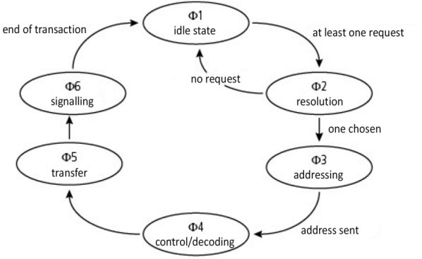
Figure 1.35. Simplified state diagram of a bus protocol
These three phases result in implementation through the following signals: Bus Request (BReq), Bus Grant (BG) and potentially a Bus Busy (BBusy) signal, or even a preemption request (Bus preempt) to remove the bus from the current holder. These are active at the low or high state depending on the implementation and technology of the logic used. These signals can circulate serially or in parallel between the nodes. A distinction can be made between several connection topologies. These are the daisy chain, the star, the bus or a mixed solution drawing on the best aspects of the different approaches. The three most common communication diagrams for receiving requests or sending out arbitration responses are the daisy chain, independent requests and polling.
The daisy chain is a type of link between communicating nodes, each with an input signal and an output signal, thus creating a chain between them. This signal can be the access grant to a bus, as is the case in Figure 1.36. This daisy chain allows for a serial distributed arbitration solution to be reached. It is distributed as each node is in possession of its own arbiter. The requests are made in parallel thanks to a wired OR. A node that wants the bus activates the request line if its BPRI (Bus PRiority In) input is not active. The other nodes propagate the request up to the requesting node, which then becomes the bus owner, while maintaining its request. Resolution is therefore conducted serially. The bus state can be read in the BPRI input. In principle, allocation is fixed by the geographical position of the nodes in the loop, and is therefore not fair. This is a simple and cheap solution, as it does not involve a lot of logic (Figure 1.40). However, it is slow because the response has to go from node to node. Another disadvantage is the complex cabling, as, for example, in the case of a backplane bus with slottable daughter cards, the continuity of the chain must be maintained. This can be done using a strap, or with a dummy board, a bit like what is done in the CRIMM16 module (Continuity Rambus In-line Memory Module, cf. § 7.2.1 in Darche (2012)). Moreover, if one of the nodes fails, some of the nodes are then isolated and therefore become blocked. A daisy chain model is studied in exercise E1.4.
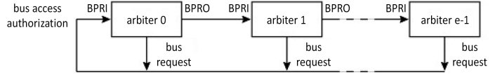
Figure 1.36. Another version of daisy chain distributed arbitration (from Thurber et al. (1972))
Figure 1.37 presents a variation on the previous version, this time with a permanent state of grant for taking the bus for the first arbiter (no. 0). If it wants the bus, and if the bus is free, it takes the bus and activates the corresponding state line. If the bus is busy, it waits for it to become free. If it does not want it, it activates its BPRO (Bus PRiority Out) output, passing its right of access to the next one along the chain.
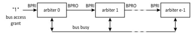
Figure 1.37. Daisy chain arbitration (variation)
Figure 1.38 shows a simpler version of this, but the state of the bus cannot be determined on a grant signal level, but rather on an edge.
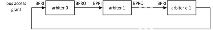
Figure 1.38. A simple solution for daisy chain distributed arbitration (from Thurber et al. (1972))
Figure 1.39 shows a centralized version. Requests are made in parallel. An access grant is given by the controller, but priority is fixed by the physical cabling of the nodes with the same weaknesses as before, which concern priority and tolerance to material faults. The entity that takes the bus and keeps the bus signals to it through the occupation line. It should be noted that if this line is removed, we revert to the daisy chain solution from Figure 1.36. Several loops or request-grant chain levels can exist in order to create a priority hierarchy (multi-level arbiter). Exercise E1.3 is an example of a study in parallel arbiters.
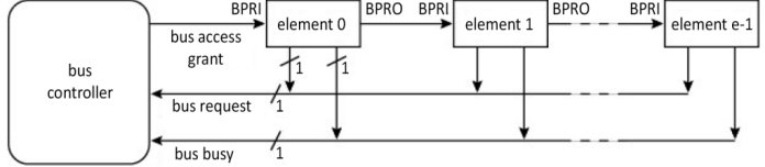
Figure 1.39. Centralized version of the daisy chain
Figure 1.40 describes the control logic at the level of each node, which blocks agreement according to priorities linked to the geographical position of the element within the bus. Spatial priority can be changed thanks to specific cabling using cavaliers or straps, as described in Borrill (1981), although this is a very onerous solution to put in place, and can result in mechanical faults. Inverters have an output that is compatible with them being placed in parallel, that is, a collector or open drain, for example. The simplicity of the flowchart should not disguise the complexity of the timescales, which need to account for all the bus delays and the processing electronics.

Figure 1.40. Daisy chain agreement bus access control logic (simplified)
The preceding example was inspired by the Unibus™ bus from the PDP-11 made by the company DEC. Figure 1.41 presents the corresponding process chronograms (positive logic). A node requests access (timestamp no. 1). Access is granted to the first node concerned (timestamp no. 2). This node acknowledges receipt (timestamp no. 3) and removes its request (timestamp no. 4), which results in the grant also being removed (timestamp no. 5). The bus becomes free (time interval no. 6) and then blocked for the transfer (time interval no. 7), and the arbiter signals this (time interval no. 8).
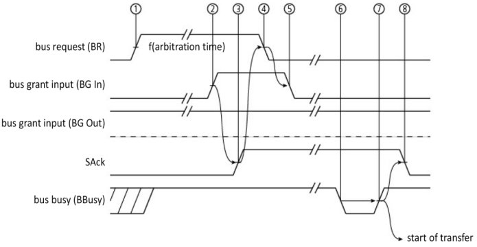
Figure 1.41. Unibus™ bus arbitration sequence

Figure 1.42. Topology of a centralized arbitration
In order to get around the major inconvenience of a chain break, an independent request approach can be used. Figure 1.43 presents a centralized version inspired by bus PCI (PCI-SIG 1998). Each request and each grant are independent of each other. They are carried out in an asynchronous manner. For this, the arbiter, or manager, must be highlighted within the bus controller as the one that receives requests and, depending on the access policies, determines which entities can get access to the bus. Examples among the commercial arbiters are the 74xxx148, 74F786 and 82C89 (by Intel). In the example shown in Figure 1.42, a couple of signals (requesti, granti) handle access to the bus. A requesting node i (i ∈ [0, 3]) generates its access request to the bus Reqi (Bus Request) and receives its grant Grti (Bus PRiority iN, sometimes called BPRN).
A priority encoder (Figure 1.43) establishes the number of the line to be served according to a given policy. The request and resolution are in parallel here. Arbitration of the VME bus is carried out in this way for n = 2, that is, for four lines of authorization request. Centralized arbitration is simple to execute, but the number of nodes is limited. The bus manager always needs to know whether there is a request currently underway, and whether the bus is busy or released, which depends on the shared signal of bus busy CBusy (for Common Busy), which is not shown. In order to avoid a shortage in the case where a node does not release the bus and another with higher priority asks for it, the bus manager can order the immediate release of the bus by deactivating its grant.

Figure 1.43. Centralized arbiter with independent request and resolution
The sequence diagram in Figure 1.44 provides an example of centralized arbitration with fixed priorities. Node no. 0 has the highest priority. The bus is free. Node no. 1 requests the bus, and is then granted permission to take it. It takes the bus, then frees it. Node no. 0 does the same. While this last node is master of the bus, node no. 1 makes a request that will always be denied while a higher-priority node (in this case, node no. 0) is in possession of the bus. When the bus has been freed, it can then take it. We can see here that fixed priority is not fair.

Figure 1.44. Example of a centralized arbitration protocol with a daisy chain response
Figure 1.45 shows the distributed version of a solution with independent requests. The requesters place their priorities along one of the lines of the request bus. This is an expensive option in terms of the width of the bus, but it is easy to set up in terms of electronics. The node in current possession of the bus deactivates the “bus assigned” signal; the node with the highest priority can then acquire possession of the bus by activating the assignment signal.

Figure 1.45. Arbitration by independent requests in a decentralized version
Polling is another option that involves cyclically questioning nodes in order to establish which is the requester (Figure 1.46). The node with the number corresponding to the current value of the counter activates the occupation line, which causes the counting to stop. Once the bus has been freed, if an access request has been made, the counter can start a poll again, either by restarting the counter or by starting again from the last node that has been granted access. The second option has the advantage of providing rotating priority, while the former provides the same as there would be in a daisy chain.
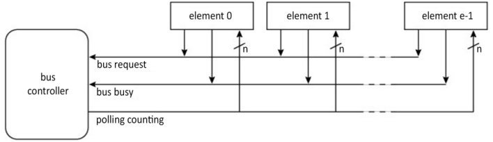
Figure 1.46. Centralized arbitration by polling (from Thurber et al. (1972))
In order to remove the request line, the counting is decentralized and a global clock signal Clk paces the counting (Figure 1.47). If a node wants the bus and the value of its counter is equal to its number, then it activates the occupation line, which results in the counting stopping. As before, after the bus is released, the counting can either return to its current value or be restarted depending on the priority policy desired. This type of mechanism is sensitive to noise.

Figure 1.47. Centralized arbitration by polling
When a node frees the bus in a distributed version (Figure 1.48), it positions the “bus free” signal and a number on the polling bus. This can represent an address or a priority. If this value corresponds to a node, the node in question activates the acceptance signal, which results in the “bus free” signal being deactivated. If this is not the case, however, counting takes place indefinitely according to the chosen priority policy until a positive response is received from one of the nodes.
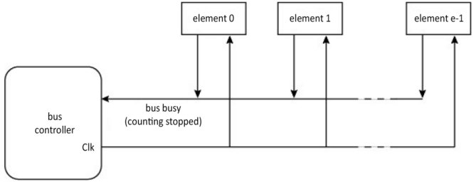
Figure 1.48. Distributed arbitration by polling
In a distributed self-selection approach, each entity is an agent in the negotiation. There is a linear version (with a linear self-selection arbiter), which has as many lines as nodes, but the number of which can be reduced with coded version (this is a coded self-selection arbiter). Here, we have an example of distributed arbitration, inspired by buses MCA (Micro Channel Architecture), S-100 (IEEE Std 696 (ANSI/IEEE 1982b)), FASTBUS (IEEE 1989) or Futurebus (IEEE Std 896 (IEEE 1994)). Access to the buses is provided synchronously (by cycle). The arbitration phases are the following: at the start of a cycle, the interested units emit the value of their priority over the bus (excluding values of zero). The address thus formed is the “logical OR” of the addresses thanks to outputs like the collector or the open drain (cf. § 2.2.1 and 2.3 in Darche (2004)). The absorbing element is therefore the value “1” when the outputs are not active. During the arbitration cycle, the units listen to the bus and change their emission to 0 (i.e. they deactivate its lines) for bits with a weight that is less than the position of the first difference (the order is MSb → LSb for Least Significant bit). The winner is the unit that recognizes the value of its priority on the bus. Figure 1.49 shows a real example of this. A major disadvantage is that the priority is fixed and therefore not fair. Kipnis (1989) formalized the protocol, and Taub (1984) describes the arbitration diagram of the Futurebus.
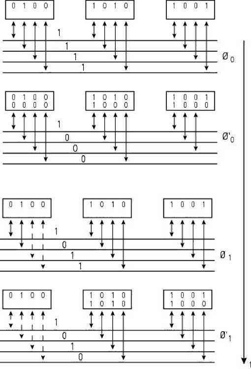
Figure 1.49. Example of arbitration distributed by self-selection
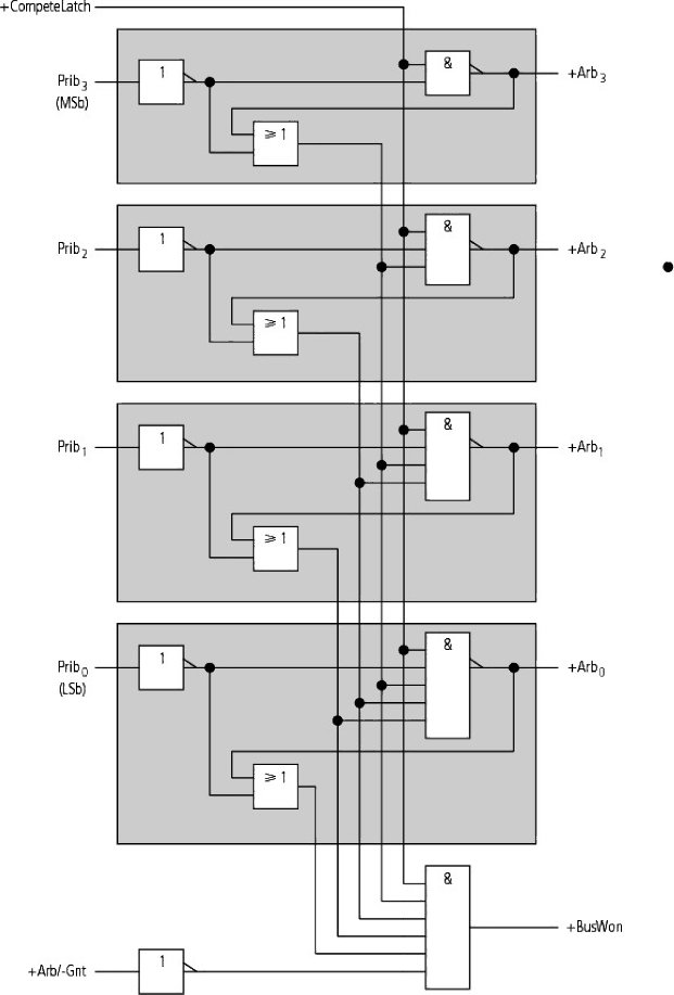
Figure 1.50. Local arbiter from the MCA bus
Figure 1.50 provides an example of the local arbiter logic, in this case from the MCA bus. A central arbiter is tasked with managing the arbitration phase by authorizing the local arbitration phase and detecting when it has ended. The arbitration serially propagates from the MSb towards the LSb. As soon as a stage i (i ∈ [0, 3]) detects that its bit with a priority of Pribi is greater than the one present on the bus (+Arbi), it causes the local election to be lost by blocking the lower AND gates.
Overlapping arbitration (anticipated arbitration) involves carrying out the arbitration for the next transaction before the current one has finished. Both Unibus™ and PCI operate with this characteristic. The property of bus parking allows possession to be retained as long as another master has not yet requested it.
Bus arbitration logic is one of the function modules of the bus interface (cf. § 3.1). A commercial example of a discrete Arbitration Bus Controller (ABC) is the TFB2010 circuit from the company Texas Instruments (TI), made for the Futurebus+ (FB+) bus, which has been standardized under IEEE Std 896 (IEEE 1994). An integrated version of the controller is the MPU NS32132 from the company National Semiconductor (NS).
In summary, the centralized option has the advantage of being simpler, but the number of nodes to be managed is limited. Distributed policies are more tolerant with regard to material faults. This obviously does not apply to the daisy chain, which is an exception. It tends to be slow, and priority usually depends on the physical position of the card on the bus. Other arbitration techniques do exist, such as collision detection and ID tokens. Collision detection is used in the field of networks through the CSMA/CD protocol (Carrier Sense Multiple Access with Collision Detection method) by Ethernet (IEEE 1985). The use of ID tokens is another technique, based on a token that goes from node to node (sequential token passing). The node that is in possession of the token can access the bus. The protocol must ensure that the token is unique. Finally, for informative purposes, the main arbitration protocols are covered in Guibaly (1989). Dandamudi (2003) created a classification of arbitration criteria, which is shown in Figures 1.51 and 1.52, which are perfect summary of the points we have made heretofore. The first one covers organization, allocation policies and bus release.
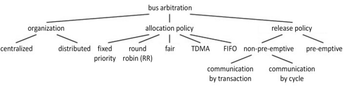
Figure 1.51. Design tree of a bus arbitration
The second figure classes the access requests and grants.

Figure 1.52. Design tree of a bus arbitration (continued and end)
1.7. Conclusion
After some general points regarding communication, the main mechanical, electrical and temporal characteristics of buses were presented. These can potentially be specified within a reference standard, which would allow for further standardization of electronic and mechanical components, thus reducing costs. Next, we looked at the notions of protocol and arbitration. Exchange by the synchronous approach was examined in great detail.
- 1 Frequency-Division Multiplexing (FDM) is not suitable here.
- 2 Some authors, Borrill (1981), for example, consider a bus to be formed of the connection of two or more elements.
- 3 An address is a digital label that takes the form of an integer, and is linked to a location or memory cell.
- 4 He adds to the definition that a bus can only be physically dedicated if a pair of elements belong to the bus and use it exclusively. We shall not keep this addition as this would be a link according to our own definition.
- 5 A counter-example is the 12-bit data format in the PDP-8/E mini-computer from Digital Equipment Corporation (DEC).
- 6 This statement is true, but it is important to remember the counter-example of the RS-232 link (EIA 1991 1997), which uses a 25-pin D-Sub connector with only eight effective signals and the ground (cf. § 8.2.2 in Darche (2003)).
- 7 The prefixes of these units must not be confused with those used for measuring the size of a memory, which we recall are: kilo (= 210), mega (= 220), giga (= 230) and tera (= 240), cf. § I-2.6.1 in Darche (2000)). There was some ambiguity surrounding the corresponding symbols. Only kilo could be represented with capital K, and all the others had to be determined based on the context. Fortunately, these prefixes have since be standardized by the IEEE ((IEEE 2002a b), cf. § V1-2.1 and § 1.1 in Darche (2012)).
- 8 Bus S-100 takes its name from the number of lines it contains. It was first used in the kit micro-computer Altair 8800 (8-bit Intel 8080 microprocessor, main memory with 256 bytes of RAM, with possible expansion to 64 KiB) from the company MITS (Micro Instrumentation Telemetry Systems), which first appeared on the market in 1975.
- 9 Synchronization through software can be a convention of characters, such as the Xon–Xoff protocol, for example, or a known or given frame length. It cannot be used for buses due to low efficiency.
- 10 Continuous time can be considered, as shown in Del Corso et al. (1986), but in practice, event discretization is preferred.
- 11 From the Greek root “meso”, meaning “in the middle of”.
- 12 From the Greek root “plesio” meaning “neighbor”.
- 13 From the Greek root “hetero” meaning “different”.
- 14 Colmenar et al. (2009) starts the transaction one phase earlier, that is, at Ack↓.
- 15 Plummer (1972) explores asynchronous arbiters, and Cowan and Whitehead (1976) presents a version with polling.
- 16 This type of link was already covered for I/O (cf. § 1.2.3 in Darche (2003)) and for memory (cf. § 5.3 in Darche (2012)).