2
Debugging and Testing
This chapter focuses on development, debugging and testing for MPUs (MicroProcessor Units) for evaluating the performance of components and microcontroller programmers. It begins by describing the first electronic boards developed by designers. Debugging is then addressed from the hardware and software perspectives. The chapter concludes by addressing the testing aspect.
2.1. Hardware support
Various systems make it possible to evaluate an MPU. Moreover, programmers have been developed for microcontrollers.
2.1.1. Generic electronic boards
Before designing an application, a developer can take advantage of a range of generic electronic boards initially provided by microprocessor manufacturers, then by third-party companies. They make it possible to evaluate components and to quickly produce demonstration programs. In increasing order of performance, and with the caveat that there are subtle differences between them, there are starter kits, evaluation boards and development boards. The first, because of their very low cost, are made up only of a microprocessor and a minimal set of connectors. Evaluation boards have a more complete set of connectors and additional peripheral components, such as a more advanced initialization circuit or components that belong to an associated family of circuits. Development boards are evaluation boards to which the necessary components have been added for developing simple prototypes, that is, additional components such as memory, for example, or I/O (Input/Output) controllers and a debugging and programming interface (cf. § 2.2.5). Subsequently, the developer can invest in a more powerful development environment with full knowledge of the relevant factors. Demonstration boards are representative realizations implementing the component. These boards are therefore an inexpensive way to get to know a product and to allow the client to determine if it is a good choice for them. Economic requirements are therefore essential. Indeed, the price must be sufficiently attractive for the client to be able to try out the component at the lowest possible cost and then buy a complete system or build their own application, if necessary. With the Internet of Things (IoT), System on Modules (SoM) appeared, which combine evaluation sensors with processing and communication electronics on a small Printed Circuit Board (PCB).
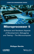
There are several evaluation boards that were the key to the success of 8-bit microprocessors. These include the KIM1 board from MOS Technology and Rockwell; the Versatile Input Monitor (VIM), renamed the SIM Model 1 (SYM-1) from Synertek Systems Corp.; the Motorola MEK6800D2; the Intel SDK85 (Figure 2.1); and the AIM 65 from Rockwell International. The first four have between 1 and 4 kibibytes of RAM (Random Access Memory), a monitor of a few kibibytes of ROM (Read-Only Memory, cf. § 2.2.4), a 16-key input for hexadecimal numbers with additional 8 function keys, 6 seven-segment LED (Light-Emitting Diode) displays, a connector providing access to all signals on the bus and a soldering or wire-wrap prototyping area, if there is one. The AIM-65 board, which was more advanced, possesses a 20-character display and a 20-column dot matrix printer with 5 x 7 dot resolution. Some had a connection to a cassette tape, which made it possible to load and save a user program in the form of a signal on an audio tape (cf. § 7.2.2 in Darche (2003))!
The current trend is towards the elimination of the aforementioned peripherals, undoubtedly for reasons of cost and development flexibility, as well as because of the integration of development-facilitating functionality. The board is now made up of the microprocessor, RAM, flash EEPROM (Electrically Erasable Programmable ROM) and a serial communication interface that is usually RS-232 compliant (cf. § 8.2.2 in Darche (2003)) for historical reasons and because it is available on all microcomputers, if necessary, by using a USB (Universal Serial Bus) adapter. The board communicates with the user through an RS-232 asynchronous serial connection (initially) and a computer, even if the aforementioned peripherals are later added based on requirements (Figure 2.2). The user therefore has access to it in addition to the computer’s resources for development. Applications are developed using a cross-compiler or cross-assembler (cf. § 1.2.1) and then simulated. They can then be downloaded for in situ debugging. The development computer can store source code, executables and memory dumps.
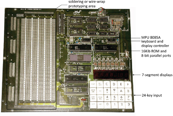
Figure 2.1. The Intel SDK85 evaluation kit. For a color version of this figure, see www.iste.co.uk/darche/microprocessor5.zip
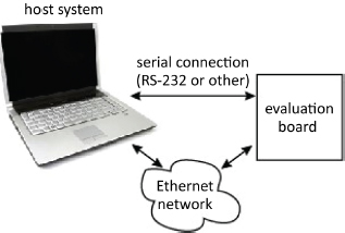
Figure 2.2. Communication between host and target systems. For a color version of this figure, see www.iste.co.uk/darche/microprocessor5.zip
Figure 2.3 shows the STK500 evaluation board for Atmel microcontrollers. For this type of component, these boards generally integrate simple input peripherals such as push buttons or outputs such as LEDs; in this example, there are eight of each.
Figure 2.3. The Atmel STK500 evaluation kit. For a color version of this figure, see www.iste.co.uk/darche/microprocessor5.zip
2.1.2. Programmers
The first microcontrollers had UV-EPROM memory (Ultra-Violet Erasable Programmable ROM, this will be covered in a future book by the author on storage) that could be erased using a quartz window on the package that let through UV light (Figure 2.4), except for the version that used OTP (One-Time Programmable) EPROM (OTPROM). An autonomous device called a programmer that was responsible for loading the program into the memory was necessary.
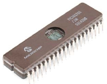
Figure 2.4. Microcontroller with integrated EPROM seen through the package’s quartz window. For a color version of this figure, see www.iste.co.uk/darche/microprocessor5.zip
Today, ROM is usually Flash EEPROM/E2PROM (Electrically EPROM) or FEEPROM/FE2PROM. Programming and erasing are done electrically. This is called In-Situ Programming (ISP). More generally, a component that can be programmed (via registers or internal memory) when it has been added to the board is referred to as In-System Configurable (ISC). The underlying board must of course have a suitable interface. Communication between the host and the target takes place via a traditional RS-2321 asynchronous communication interface (cf. § 8.2.2 in Darche (2003)) using an integrated program or via a debugging interface (cf. § 2.2.5). The latter can be used for debugging. Figure 2.5 shows the ISP/PDI interfaces (Program and Debug Interface) used in the Atmel STK600 evaluation kit.
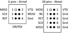
Figure 2.5. ISP and PDI interfaces for the Atmel STK600 evaluation kit
The IEEE 1532-2002 (IEEE 2003) standard specifies programming for configurable components. The state machine managing the programmable component has two primary states, system and test (Figure 2.6). The system state is used for normal operations (i.e. initial), even if non-intrusive commands can be executed. The test mode enables control of the component’s I/O pins to allow programming of memory, for example.
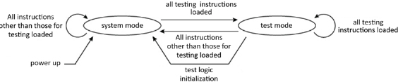
Figure 2.6. Management state diagram compatible with the IEEE 1149.1 standard
The four standard-required instructions are ISC_ENABLE, ISC_DISABLE, ISC_PROGRAM and ISC_NOOP. The first two (de)activate the programming environment. The next enables system programming. The last makes it possible to put the system into idle mode (NO OPeration) in the case of parallel programming. The optional programming instructions are ISC_READ, ISC_ERASE, ISC_PROGRAM_USERCODE and ISC_DISCHARGE. For control and security, the optional instructions are ISC_PROGRAM_DONE, ISC_ERASE_DONE and ISC_PROGRAM_SECURITY. Instructions for accessing an address field or optional data are ISC_READ_INFO, ISC_DATA_SHIFT, ISC_SETUP, ISC_ADDRESS_SHIFT and ISC_INCREMENT. Ten standardized registers have been associated with these instructions. Figure 2.7 presents their relationships with the aforementioned registers.
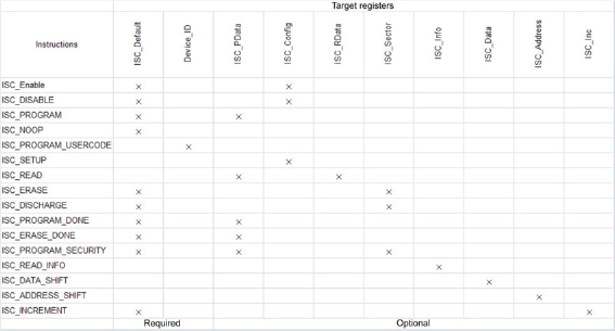
Figure 2.7. Compatibility between standardized instructions and target registers
At the hardware interface level, this standard relies on the IEEE 1149.1 standard, which includes the JTAG (Joint Test Action Group, cf. § 2.2.5) interface. It is also necessary for managing programming-specific signals.
2.2. Debugging
Debugging2 for a processor-based system involves searching for and resolving faults and errors, both in hardware and software, during the development, tuning, production and running phases. It is important to distinguish pure hardware or software approaches from hybrid approaches.
2.2.1. Evolution
Hardware debugging and testing for microprocessor board(s) was initially carried out primitively using solid or blinking LEDs, or – a slight improvement – with messages on LEDs or LCDs (Liquid Crystal Display). A parallel port could be used to produce a binary number representing an error code, as was the case with the first IBM PC (Personal Computer, cf. § 3.2.1) during POST (Power-On Self-Test, cf. § 3.5.3). Some motherboard manufacturers still offer this functionality in the form of one or more seven-segment LED displays. These POST codes are sometimes associated with a set of audio beep codes. A final primitive approach is to program system memory, observe the application’s operation and potentially debug it by iterating over these three steps as long as the system is not functioning correctly. This method is referred to as burn and learn, and is only applicable to small microcontrollers. Microprocessor system debugging has become complex with the integration of several levels of cache and acceleration mechanisms such as pipelines (this will be covered in a future book by the author on microprocessors). It is also important to note that debugging electronics that originally functioned at the board level are now integrated at the chip level. The complexity of debugging is still increasing.
At the software level, calls to message sending routines (internal system state) for signals or errors via the RS-232 serial connection (the traditional console) were inserted, either conditionally or unconditionally, in the application code, similar to the printf() debug print statement in C using preprocessor directives such as #if. Small programs can also generate observable events on an analog oscilloscope. For example, a sequence of nop (no operation, cf. § V4-2.8.5) instructions increments a sequence counter, which is observable on the address bus (cf. exercise V4-E2.6). Another example is a loop including a complementary state change3 (toggle mode) for an I/O port pin, which will manifest via a rectangular signal. Professionals quickly realized the need for more powerful approaches.
2.2.2. Functionality
Debugging is relevant to every language level, from machine language to assembly and high-level source code (source level debugging). The debugger’s functions can be divided into two groups, those for runtime control and those that enable system access. For the former, the fundamental functions are execution start and stop, single-step mode execution, and breakpoint placement, which can be synchronous with an instruction, simple (i.e. unconditional), complex or temporary (goto command), and their detection. Instruction tagging makes it possible to stop the execution of a program when the marked instruction is reached but not executed by the MPU and to return to debugging mode (cf. § 2.2.5). The breakpoint mechanism is based on a comparison of an address value or data depending on its type in relation to a reference. The breakpoint can be managed via hardware or software. In the case of variable-length instructions (the fixed-length case is trivial), it is useful for debugging to determine the instruction boundaries in the machine code (interruptible “at the instruction boundaries,” cf. § V4-1.1).
For improved speed, as a complement to the traditional step-by-step execution mode, a special step-over mode makes it possible to execute subprograms in normal mode, while the rest of the program is running in step-mode. It is important to distinguish between three types of breakpoint: execution breakpoints, memory breakpoints (triggered by read/write or by a defined value) and I/O breakpoints on a port or event basis. Some debuggers also distinguish between the execution modes of user-mode debugging and kernel-mode debugging. The word synchronous means that there are no more instructions executed after the one immediately preceding the requested stop. With a complex breakpoint, it is possible to specify a range of addresses or to use a logical mask. A logical condition can also be used to trigger the stop. These functions for controlling execution then enable access to information. Thus, during an execution stop, they allow observation and modification of the microprocessor’s internal (registers and internal memory) and external (memory areas) resources. It is also possible to place breakpoints on data. There are also watchpoints that can be set on an instruction, a value, an address reached in memory or the value of a register, which is identical to a breakpoint except that it does not stop execution but triggers the sending of a message sent to the debugging tool. It should be noted that the function at the root of a breakpoint or watchpoint is comparative. Monitoring instructions are especially important in the real-time domain where it is difficult to capture events. The difference between hardware and software breakpoints for instructions lies for the former in the fact that they are limited to RAM if the memory overlay functionality is not used. For an instruction breakpoint, also called an execution or program breakpoint, the debugger replaces the instruction from the target address with a rerouting instruction, generally a trap (cf. § V4-5.4), which stops the application and re-routes the instruction flow to the debugger. For the hardware version, specialized electronics detect the binary patterns that are stored in specialized registers in a wave, or, today, in the MPU. Both types are synchronous. Event and access breakpoints are asynchronous. Huges and Sawin III (1978) describe the technique for a software breakpoint.
Advanced capture functionality involves tracing the execution of instructions, access to data in memory and events such as hardware and software interrupts (cf. Chapter V4-5, i.e. exceptions) Tracing consists of real-time storage of a set of information (instructions, data, addresses, etc.) related to execution. It then allows a debugging tool to replay the execution, which renders the system externally observable. To increase execution speed, this information must be compressed on-the-fly. Its value lies in obtaining information prior to an error rather than just after, as is the case, for example, with a breakpoint, which then enables analysis at the error breakpoint. It requires significant memory resources, relative to the historical amount required. Execution traces are recorded by a logic analyzer or another suitable tool. To limit the message size (frame) and the transmission time, these can also be compressed.
Source-level debugging facilitates program tuning. The debugger can also grant access to the corresponding code in assembly language, which is useful when optimizing compiler-generated code. Furthermore, dynamic Performance Analysis (PA) can be provided for analysis; for example, the number of interrupt requests or calls to a subprogram, or the failure rate for the various cache levels. The debugger can also provide memory or I/O emulation.
Debugging becomes more complicated in the presence of an Operating System (OS) and, even more so, for real-time applications. The most powerful debuggers can trace system calls, for example.
Debugging a System on (a) Chip (SoC, cf. § V1-1.2 and V2-4.10) is the most complicated type. Debugging an embedded system is difficult because, unlike a computer, it does not usually have advanced peripherals such as a keyboard or monitor. Furthermore, the signals on the PCB are no longer available because the system has been integrated. To debug this kind of component, it is necessary to be able to control the execution (start, stop and step-by-step) and to manipulate (i.e. read/write) the MCU’s4 registers and memory from an external tool using a communication interface. To this functionality, we must add ROM emulation by RAM (loading) and real-time analysis of the instruction flow with tracing.
By building on the notion of class in the IEEE-ISTO 5001™-1999 standard (IEEE-ISTO 1999), four classes of debuggers can be defined. Class 1 provides basic functionality, that is, execution control (start/stop/step-by-step), with breakpoint and watchpoint insertion from which it is possible to access registers and, in memory, the variables and constants, and to read and write when necessary. The half-duplex dialog between the host and the target occurs via a test interface with a limited throughput (cf. § 2.2.5). The second class adds program and membership tracing (of a running function or process for an OS) via an auxiliary interface. This auxiliary port is shared with slow I/O, and as such has limited bandwidth. Class 3 enables read/write operations in memory and tracing of data writes in memory on-the-fly, that is, without stopping execution. I/O on the auxiliary port becomes fast. The last class authorizes memory substitution via the auxiliary port and watchpoint-triggered tracing. Data read tracing in memory is also possible. Table 2.1 reviews the incremental characteristics of these classes.
Table 2.1. Incremental characteristics of classes of debuggers
| Classes of debugger | ||||
|---|---|---|---|---|
| Characteristics | 1 | 2 | 3 | 4 |
| Runtime control | JTAG interface | JTAG interface | JTAG interface | JTAG interface |
| Communications | Cross-band (limited throughput) | Full-duplex (high throughput) | Full-duplex (high throughput) | Full-duplex (high throughput) |
| Auxiliary port | No | Yes shared with slow I/O pins | Yes shared with fast I/O pins | Yes shared with fast I/O pins |
| Trace storage | Not supported | Yes Execution via auxiliary port | Yes On-the-fly execution Data write tracing On-the-fly memory read/write (MEMR/MEMW) via auxiliary port | Yes On-the-fly execution Checkpoint triggers via auxiliary port |
| Data acquisition | Not supported | Not supported | Yes | Yes |
| Memory substitution | Not supported | Not supported | Not supported | Data read via auxiliary port Substitution trigger via watchpoint (optional) |
2.2.3. Hardware emulators
A hardware emulator intervenes between the host and target system. It makes it possible to mimic the behavior of hardware. In the context of our study, a microprocessor is replaced by an external hardware device equipped with a specialized probe that will generate signals from the latter. It therefore emulates its internal operation and signals from the electrical and temporal points of view. By redirecting the microprocessor’s functionality, it becomes possible to isolate it for better observation and control of its operation, which facilitates both tuning of the electronics board under development and its future maintenance. Its functions are mentioned above. It can also store a real-time execution trace. It can also provide a memory space in place of or complementary to the application’s space (overlay memory). This memory area, which substitutes for the target system’s memory, allows the user to reload the application code or to patch it (i.e. to apply a patch without having to repeat the software development chain, namely compilation, assembly and link editing) without having to program the microcontrollers or the system. This area can furthermore replace a memory area for a system that is not yet present. The exact name is “emulator on user circuit.” Intel uses the term In-Circuit Emulator (ICE); Intel also developed the ICE-80, nicknamed the blue box. These emulators were initially connected to a system or a logic development station (per HP’s terminology). For example, the ICE-80 was associated with the Microcomputer Development System (MDS) 80. Another well-known example is the HP 64000 workstation from Hewlett-Packard. This architecture is described in Kline et al. (1976), Krummel and Schult (1977), and Stiefel (1979). These systems were an expensive solution because the electronics were complex and because the systems were cumbersome. Today, they have been replaced by the microcomputer (Figure 2.8). An emulator can be referred to as universal, becoming specialized for a given microprocessor by adding a module containing the latter’s electronics.
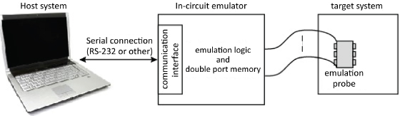
Figure 2.8. Hardware emulation chain. For a color version of this figure, see www.iste.co.uk/darche/microprocessor5.zip
Four operating modes can be distinguished: free-running mode, debugging, monitoring mode and step-by-step. In free-running mode, the target runs at full speed, and the debugger waits for a command to take control. In debugging mode, the microprocessor is stopped, and the debugger executes the debugging commands. In monitoring mode, the target runs at full speed, but the debugger monitors the breakpoints and watchpoints. As soon as one of these points is reached, the debugger switches to the preceding mode. In the last mode, the system alternates between monitoring and debugging modes for each instruction executed.
The core of the emulator is generally a microprocessor identical to the one on the board under development, with the exception that some of its internal control, state, and bus signals, etc., are externalized (bond-out chip). Internal registers such as the Program Counter (PC) are also accessible. All of these additional points of access make it easier to precisely know the component’s internal state and to control its operation. They also enable implementation of function traces (cf. § 2.2.2). This type of component is provided by the manufacturers themselves to the manufacturers of emulators. The problem of commercial availability therefore arises, and its solution is a function of market size. Adding an emulator has an impact on the target’s performance. For each signal, an additional delay is generally inserted, and an electrical charge is added (cf. § 3.6 in Darche (2004)). The emulator generally runs at a lower frequency than the real component and does not exceed hundreds of MHz, especially if the emulated microprocessor is replaced by equivalent discrete logic or, today, by FPGA (Field-Programmable Gate Array) type programmable logic circuits (cf. Chapter 4 and, more specifically, § 4.3.2 in Darche (2004)).
The logic (state) analyzer and the digital oscilloscope are devices for measuring and visualizing complementary signals, especially now that they include protocol analyzers.
Today, this traditional approach is disappearing because components have increased operating frequencies exceeding GHz, and they have hundreds of pins, or even thousands nowadays (i.e. after 2006). Only those microcontrollers with a limited number of pins can still be emulated in this way. Furthermore, modern microprocessors and microcontrollers also include debugging and testing electronics (cf. respectively § 2.2.4 and § 2.3). Emulation has evolved from an ad hoc to a standardized, retargetable solution with the use of a standard interface (cf. § 2.2.5).
Today, given the ability to put an entire system onto a chip (i.e. SoC), emulators are typically embedded. The ARM7/TDMI embedded processor was one of the first circuits with integrated ICE (EICE for Embedded ICE).
Finally, for reference, there are RAM and ROM emulators that have double access ports. The first is accessible by the target, and the second by a probe that can read, write or program depending on the memory type.
2.2.4. Software debugging
Historically, software debugging was done post mortem by analyzing memory contents (core dump) in the form of a paper printout (i.e. listing). The debugging monitor was the first embedded software (FirmWare or FW, cf. § 3.5.1), which assists with tuning. Today, it is important to distinguish between standalone software debuggers and those assisted by a hardware device that controls the processor.
2.2.4.1. Debugging monitor
Historically, microprocessor evaluation boards were equipped with software called a debug monitor for managing the board. This was a program resident in ROM (ROM monitor) for launching and tuning applications. It managed various controllers and peripherals for a microprocessor system (keyboard, displays, serial connection). The corresponding service routines were made available to the developer for their applications. It also made it possible to load, launch and update user programs. To do so, a command interpreter associated with a dedicated communication interface read command inputs and provided recording and branching for the corresponding system process. After execution, a report was displayed on the traditional output (displays, screen, etc.)
As examples, we will mention the JBUG/MINIBUG II and BUFFALO monitors (Bit User Fast Friendly Aid to Logical Operation) respectively for the Motorola MEK6800D2 and M68HC11EVB boards. MINIBUG is firmware that makes it possible to load and launch a memory dump. It can list the contents of registers and modify a memory location. Table 2.2 reviews the general characteristics of these early monitors. It should be noted that the monitor could be included in boot ROM. Thus, the notion of a monitor is found in microcomputers such as Macintosh or in SUN workstations, some of which included a basic monitor that provided terminal functions, allowing, among other things, reinitialization, MPU register and memory access, and the boot support definition (cf. § 3.5.3) with the help of input commands.
Table 2.2. Generic characteristics of a debugging monitor
| Characteristics | Generic debugging monitor |
|---|---|
| Software aspects | Firmware on target |
| Intrusive | Yes – monitor resident in user space User code patch for breakpoints Keyboard-display or access port required to communicate with the host |
| Code download | Yes |
| Execution commands (run/stop/step) | Yes |
| Code breakpoint | Simple only (generally software) |
| Data breakpoint | No |
| Access | Processor registers/variables |
| On-the-fly access | No |
| Observation point | No |
| Real-time tracing | No |
| Clock and timer | Can be used in step-by-step monitoring mode |
| Wait and stop modes | Monitoring mode not accessible in these two modes |
| Communications | RS-232 protocol, standard PC data rates |
| Cost | Low |
| Advantages | Simplicity/cost/broad family support |
| Disadvantages | Intrusive/only basic debugging functionality |
Table 2.3 shows the main characteristics for a representative monitor, the Motorola MCU HC08.
Table 2.3. Primary characteristics of the HC08’s monitor mode (Motorola)
| Characteristics | HC08 monitor mode |
|---|---|
| Input in mode | At least four generic I/O pins (V+ on IRQ signal) |
| Communications | RS-232 protocol (NRZ), standard PC data rates |
| Software | Firmware on target |
| Commands | Number = 5 Indirect access to MPU registers Access to memory only in monitoring mode |
| Breakpoint | One associated function |
| Clock or timer | Active in monitoring mode |
| Wait and stop modes | Monitoring mode not accessible in these two modes |
| Debugging connector | 16-Pin MON08 |
It is important to distinguish between the monitoring functions of user mode and supervisor or monitor mode. The latter can be emulated if the microprocessor does not have execution privileges.
The monitor uses the board’s resources, specifically the read-only (monitoring program) and random-access (workspace) memory spaces and some I/O controllers (serial, parallel, etc.). The monitor is generally installed with the interrupt vector table (cf. § V4-5.7) or, at least, the initialization vector (reset). Figure 2.9 shows an installation at the top of the address space for an MPU like the MC68xx with Motorola’s BUFFALO monitor. The interrupt vector table can be found at the top of the address space (typical case for 8-bit MPUs) or at the very beginning.
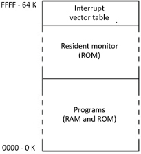
Figure 2.9. Memory location of the monitor
2.2.4.2. Software and in situ simulators
A simulator is a software that imitates a component’s behavior. It makes it possible to test a user program without interacting with the hardware. The effectiveness of this approach is limited, but it enables debugging of the most serious errors. As with a debugger, the user can see on the display (Figure 2.10) the register set for the microprocessor, the memory areas including the stack, interrupt table, data area (i.e. variables) and the area for instructions. In the latter, the program exists in the source language, generally a High-Level (programming) Language (HLL) such as C, or in assembly. In the case of a microcontroller (Figure 2.10), the registers of the I/O controllers as well as the state of the peripherals are also shown. Besides than step-by-step and continuous modes, the program can also be executed in conditional mode (instruction or cycle counter, logical conditions) by simulating input–output controllers and memory such as the cache. It is also possible to set breakpoints. This can help detect invalid operation codes. Some simulators provide statistics such as the average number of loops or the number of times a variable is accessed; with this information, the user can optimize their program. This tool is provided in addition to others such as a hardware emulator (cf. § 2.2.3). It also offers obvious pedagogical utility.
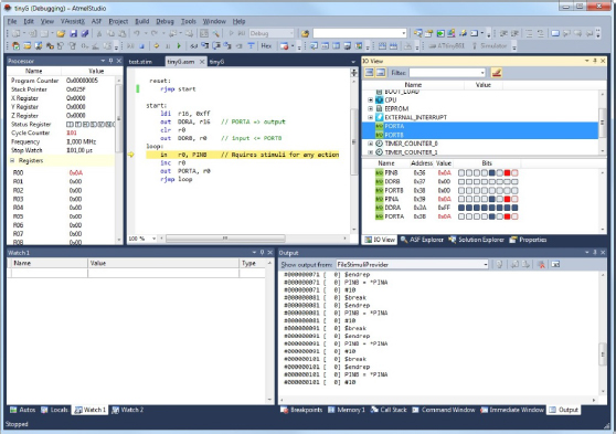
Figure 2.10. The Atmel Studio simulator. For a color version of this figure, see www.iste.co.uk/darche/microprocessor5.zip
One example of a mixed hardware–software simulator is the In-Circuit Simulator (ICS), which exists between a software simulator and a hardware emulator (cf. § 2.2.3). It is used for microcontroller-based development. The hardware part is made up of a traditional communication module, including the same microcontroller as the target, and is installed using a probe. It simulates operation by executing the application, but not in real-time. This allows an ICS to interact with the target’s I/O, which adds new functionality. All software development tools and simulators can then be used.
Given the increasing complexity of hardware, and in order to facilitate hardware/software co-development, a high-level model can be constructed, for example, in C. The system state then exposes itself in the form of variables with unrestricted access, which facilitates testing. The primary disadvantage is that this approach does not take real-time issues into account.
2.2.4.3. Software debugging
Modern processors, beginning with the 16-bit generation of microprocessors (or 8-bit for microcontrollers), now include some of the functionality of a hardware emulator, such as a step-by-step mode. For example, the Intel x86 family includes a binary indicator called a Trap Flag (TF, cf. § V3-3.1.5.6) in its status register, which, when set to 1, puts the processor into step-by-step mode (trap into ICE). This mode traces a program’s execution by requesting an interrupt (into 1) after the execution of each instruction. A software debugger can then take over to monitor execution. Previously, this functionality didn’t exist; in the case of microcontrollers, an alternative was to use a clock that would trigger an interrupt request after a number c of cycles corresponding to the execution time of the next instruction (example from the BUFFALO monitor associated with the OC5 (Output Capture) clock in the MCU HC08). Moreover, software breakpoints can be inserted in the form of dedicated int 3 interrupt requests, with the help of the two associated debug registers, DR6 and 7; in this case, the CCh machine code replaces the initial instruction. Other processors can use a traditional software interrupt request (e.g. HC11’s swi in the Motorola BUFFALO monitor). For each request, there is a corresponding interrupt vector that contacts the start address for the debugger (interrupt handler). The disadvantage is that the user program is modified by replacing an instruction with a software interrupt request.
Today, this tool enables program tuning by helping find errors (bugs). It uses a testing interface (cf. § 2.2.5) that makes it possible to interact with the processor. Just as a system or a component, a microcontroller, for example, may integrate flash EEPROM; the debugger includes the functions of memory erasing, programming and checking. The debugger is sometimes called a “software emulator,” but the term can be misleading because the additional integrated software circuits (hardware debugging support) are not the same as those in a hardware emulator. They only make it possible to access the circuit’s I/O. It is better to refer to them as On-Circuit Debuggers (OCD)5.
These provide the same functions as an emulator (cf. § 2.2.3). They make it possible to start and stop execution at any point using either conditional or unconditional breakpoints, as well as watchpoints. These points can be hardware- or software-related. For the latter, a comparison of the value of the sequence counter for the processor being analyzed with the stop address occurs in real-time. Their number is limited by the hardware. A software breakpoint is carried out by inserting a stop instruction (break, for example). It is therefore highly intrusive because it modifies the application code. The most advanced display source code in a high-level language as well as the corresponding code in assembly language (multilevel debugging), which requires a disassembler integrated with the object code. Figure 2.11 shows an example. As a final type of functionality, we should mention the patch assembler, which makes it possible to modify machine code during debugging without having to reassemble the source. A profiler makes it possible to generate static and dynamic statistics and performance measurements for application functions for the purpose of potential optimization, for example, but using assembly language in place of a high-level language.
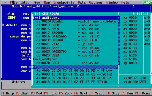
Figure 2.11. The Borland TurboDebugger. For a color version of this figure, see www.iste.co.uk/darche/microprocessor5.zip
2.2.5. Hardware support and debugging interfaces
To facilitate debugging, an MPU can integrate specialized logic and registers. This is referred to as internal or on-chip debugging. In effect, mechanisms such as an internal cache mask the microprocessor’s operation, because external observation of the bus is not correlated or, more precisely, is delayed from internal operations. Moreover, the technology of encapsulation has evolved, and the connection of a probe to capture the processor’s signals has become difficult, while attaching a probe for an emulator with a BGA-type package (Ball Grid Array, cf. § 3.3.1 in Darche (2004)) is impossible.
An example is the x86 architecture beginning with the 80386, associated with the RF (Resume Flag), 86 Debug Registers (DR[7:0] used in part for hardware breakpoints in linear address space. DR[3:0] stores the addresses for four breakpoints simultaneously in memory space or in I/O (cf. § 2.3 in Darche (2003)). DR7 and DR6 are the registers for control and debug status respectively. RF suspends undesirable debugging exceptions while the debugger is being used. The OCD is transparent with respect to the MPU’s operations. To implement this elegant solution, it is necessary to have an interface for communicating between the debugging tool and the system to be debugged. Solutions such as the traditional series, parallel and network interfaces are invasive because they use the target’s resources. The transparent solution is to use a JTAG port designed for debugging.
Test interfaces make it possible to offer system access points, which are generally serial. They have debugging functions and, potentially, make it possible to program flash memory (in the case of a microcontroller, for example). A debugging module is inserted between the host and the target, just as with an emulator. It contains the debugging controller, which will generate the signals for the debugging interface. A set of debugging commands is associated with this interface. The host transmits commands and data, which are sent to the target via the debugging interface to be executed. If necessary, it receives the data and a state. The interface on the host side is traditional, either parallel, serial or network (Figure 2.12). We should mention the DSP56000’s On-Chip Emulation (OnCE™, Motorola 1992), which enabled a specialized interface to interact with the DSP (Digital Signal Processor) in order, for example, to read from registers and memory. This DSP’s debugging mode was therefore activated by a specific input signal called #DR, either on reset or normal execution mode. It should be noted that specific instructions – stop and wait – also enable this (cf. § V4-2.5.2).
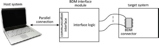
Figure 2.12. Debugging link with BDM access (HCS08/RS08 target system). For a color version of this figure, see www.iste.co.uk/darche/microprocessor5.zip
Each manufacturer initially specified its own interface (debug or probe port) with changes over the generations (families) of components. There are therefore proprietary interfaces such as Motorola’s that use a full-duplex synchronous interface called BDM (Background Debug Mode). This enables communication with some of their microprocessors and microcontrollers, such as the M68HC08/12/16. It is made up of three signals (Figure 2.13), which are DSCLK (Data Serial CLocK), DSI (Data Serial Input) and DSO (Data Serial Output). Along with a set of commands, this interface enables read and write in a specific register or in main memory and checking of other functions connected to in-circuit debugging such as initialization, start at an address, insertion of a hardware breakpoint, or memory dump or load. The message exchange format is 17 bits. This interface was the first to be used for OCD.
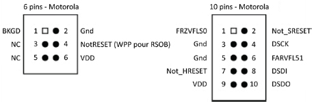
Figure 2.13. BDM interface signals
Table 2.4 shows the debugging mode characteristics associated with this interface. It should be compared with those from the monitor presented in § 2.2.4.1 (Table 2.3).
Table 2.4. Characteristics of the background debugging mode for Motorola HCS08 and RS08 microcontrollers
| Background debug mode (BDM) | ||
|---|---|---|
| Characteristics | HCS08 | RS08 |
| Input mode | Single dedicated pin (BKGD) required (no V+) | Single dedicated pin (BKGD) required (no V+) |
| Serial communication | Dedicated protocol | Dedicated protocol |
| Software aspects | No firmware on target | No firmware on target |
| Hardware aspects | External debugging module BDC (Background Debug Controller) registers Outside user address space | Interface module BDC registers Outside user address space |
| Commands | Number = 30 17 active in BM and 13 non-intrusive Direct access to MPU internal registers in active BM Non-intrusive access to memory in BM and during execution of a user program | Number = 21 10 active in BM and 10 non-intrusive One in both modes Direct access to MPU internal registers in active BM Non-intrusive access to memory in BM and during execution of a user program |
| Breakpoint | One hardware and one instruction trace Two breakpoints supported by the external module | One hardware and one instruction trace |
| Clock and timer | Inactive in active BM | Inactive in active BM |
| Wait and stop modes | Authorized background access | Authorized background access |
| (Debugging) connector | 6-Pin BDM | 6-Pin BDM |
We should mention, in no particular order, the AMDebug™ (12 pin, improved JTAG) interface, the Arm Debug Access Port (DAP) interface, Atmel’s aWire, PDI, and debugWire, NEC’s N-Wire, Motorola’s OnCE™, SDI (Serial Debug Interface), and SPI (Serial Peripheral Interface), and finally, TI’s MPSD (Modular Port Scan Device).
The IEEE 1149.1 (IEEE 2013) standard specifies the test logic to be included in an Integrated Circuit (IC) to enable testing of the interconnections between ICs once they have been soldered to the circuit board or to the component itself. It also enables observation and modification of the component’s activity in normal operation. This testing architecture is non-invasive. For this purpose, a general-use, serial-type Test Access Port (TAP), also referred to as a JTAG interface (Joint Test Action Group), in reference to its origins, is also specified to enable communications between the board being observed and the test system (Figure 2.14). Internally, additional circuit-limiting logic enables the application of test vectors and the receipt of results. Its architecture is sufficiently generic to make it possible to leverage its initial test functionality for debugging. It is possible to monitor and alter the processor’s internal logic state. Thus, the set currently offers three functions, which are boundary scan testing, in situ debugging (OCD) and memory programming.
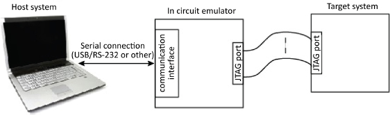
Figure 2.14. Debugging connection using a JTAG port. For a color version of this figure, see www.iste.co.uk/darche/microprocessor5.zip
The principle of peripheral boundary scan testing relies on a chain of serially linked test modules (Figure 2.15). It enables testing of the continuity of the external connections between logic systems and between a system’s logic circuits, as well as also internally at the logic block level. A test module is made up of two kinds of registers, test data registers and instruction registers. Instruction registers receive the commands to be executed. Management is granted to a controller (TAP controller), which manages the testing phases based on a 16-state state machine (cf. § 3.7.3 in Darche (2002)). There are four, or optionally five, interface signals. There are input and output instructions and test data signals respectively TDI (Test Data Input) and TDO (Test Data Output), the test clock signal TCK (Test ClocK), the TMS (Test Mode Select) mode signal and, potentially, the nTRST (Test ReSeT) initialization signal, which is active at a low level. TDI makes it possible to enter instructions and data serially into the circuit, sampled at the rising edge of TCK. TDO makes it possible to extract data. TMS makes it possible to change the state machine’s state. TCK is the sampling signal for the TMS signal and the strobe signal for data and instructions. The transfer speed is not greater than 100 MHz, which limits real-time debugging. The asynchronous nTRST signal, when it is at a low level, enables initialization of the controller.
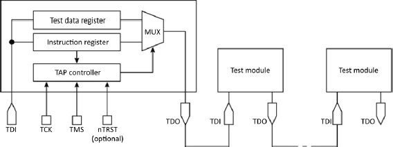
Figure 2.15. A chain of test modules.
Internally, communication relies on a chain of Boundary-Scan Cells (BSCs) surrounding the circuit being tested, corresponding to one cell per I/O pin on the original circuit (Figure 2.16). The scan path principle is a widespread testing technique. It was proposed by Williams and Angell (1973) for reading and setting a state in a logic system. The testing technique relies on a derivation of signals with the aid of multiplexers and flip-flops, the latter of which can be placed in series to form a Shift Register (SR, cf. § 3.5.3 in Darche (2002)) for the transport of test information. This peripheral chain forms the Boundary-Scan Register (BSR), which is one of the five testing data registers, which is required, as are the IDR (IDentifier Register) and the Bypass Register (BR).
The IDR register provides an identifier for the manufacturer, the circuit and its version, in 32-bit format. As the name suggests, the BR register enables direct passing of a bit entered by TDI to the TDO. The two others, which are optional, are the scan-path and BIST registers (cf. § 2.3). As an example, consider the BSR for the Motorola MPC8xx family of microcontrollers, which has a 475-bit format for testing all of its signals7 (McEwan 2002).
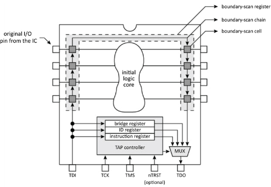
Figure 2.16. JTAG logic around the initial core
A boundary-scan register cell makes it possible to observe and control the DUT’s (Device Under Test) external input and output signals. Using a multiplexer controlled by the TAP controller (Figure 2.17(a)), the incoming or outgoing signal on the pin of the circuit to be tested can pass through transparently or can be taken charge of by the flip-flop network. Figure 2.17(b) shows an example implementation. The M2 multiplexer selects the signal path, whether normal or under test. The M1 multiplexer selects the input signal for observation or the one to be inserted. It is then taken over by two serial flip-flops, R1 and R2. The first (R1) is the capture flip-flop and the second (R2) is the update flip-flop, which is optional. Each cell is linked by Scan_In/Scan_Out signals, thus forming the boundary-scan test path.
There are 18 instructions that are either public or private. There are four required public instructions, which are BYPASS, SAMPLE, PRELOAD and EXTEST. The optional public instructions are INTEST, RUNBIST, CLAMP, IDCODE, USERCODE, ECIDCODE, HIGHZ, INIT_SETUP, INIT_SETUP_CLAMP, INIT_RUN, CLAMP_HOLD, CLAMP_RELEASE, TMP_STATUS and IC_RESET. Each manufacturer can also define its own instructions. A standardized language called BSDL (Boundary-Scan Description Language) has been proposed.
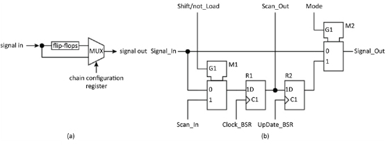
Figure 2.17. A typical boundary-scan register cell (a) with an example implementation (b)
Initiated by Hewlett-Packard in 1989 (Parker 2002), it is based on the standardized VHDL (Very High Speed Integrated Circuit, VHSIC) Hardware Description Language (IEEE 2000, also cf. Darche (2002)). More details on its internal operation are given in Maunder and Tulloss (1990).
Each manufacturer proposes a connector that includes at minimum the standard’s four or five signals. In practice, the connector has 10–20 pins (Figure 2.18). The SWD (Serial Wire Debug) interface from Arm® is a subset of the JTAG interface. It should be noted that the RTCK (Return TCK) signal is not standardized. We should also point out the ITP (In-Target Probe) interface from Intel.
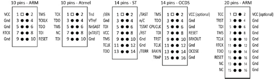
Figure 2.18. JTAG connector examples
With the spread of SoCs, which make it possible to integrate an entire system onto a chip, testing and debugging have become excessively complicated. Previously, all signals between chips were accessible at the board level and could be observed by traditional measurement instruments such as logic analyzers or oscilloscopes, or by the aforementioned debugging systems. Today, these tools must adapt to technological progress and become integrated at the chip level. Debugging an SoC requires observing, in addition to the operation of one or more processors, the internal bus (cf. § V2-4.10) and the system’s peripheral circuits, which makes it extremely complex. The traditional approach using the JTAG interface is no longer suitable. An On-Chip Debug System (OCDS) embedded in the SoC is required. This approach is presented in Stollon (2011). To respond to this problem, the IEEE 1500™ standard (IEEE 2005; IEEE/IEC 2007) revisited the idea of the IEEE 1149.1 standard to adapt it to SoCs. Around the component, we find peripheral logic, shown in Figure 2.19. A three-signal interface enables communication. These latter are referred to as Wrapper Serial Output (WSO), Wrapper Serial Input (WSI) and Wrapper Serial Control (WSC). The Wrapper Boundary Registers (WBR) enable access to the cores (i.e. logic blocks) whose operations are controlled by events (four options: delay, capture, update and transfer). Instructions such as bypass, preload, etc. are passed via the Wrapper Instruction Register (WIR). They determine the state of the wrapper. DaSilva et al. (2003) describe their operation. WBY (Wrapper BYpass Register) enables a short-circuit of the test logic.
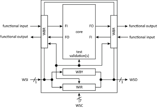
Figure 2.19. Components required by the standard
To capture a trace, that is, to capture information on-the-fly without stopping the system, the aforementioned interfaces are not suitable. An additional trace port interface must be added, as proposed in the Nexus standard (IEEE-ISTO 1999), which named it the auxiliary port (unidirectional). Another solution is to use internal memory. This port is a proprietary solution such as the Debug Communication Channel (DCC) or the trace port for ETM (Embedded Trace Macrocell) embedded logic from Arm®.
Other proposals exist, such as the MIPI (Mobile Industry Processor Interface) Alliance and the OCP-IP (Open Core Protocol International Partnership). They are not described here because they are outside this work’s scope. Vermeulen et al. (2008) take stock of these standardization activities.
In the XScale® architecture, Intel mixes JTAG technology with the monitor-type approach by downloading an image of a debugging exception manager into a reduced-size cache (2 KiB) reserved for this purpose. The JTAG interface is here diverted from its testing role to serve only as the serial communication interface. The manager is called using the traditional debugging interrupt. We have here the typical functionality of a debugger with read/write of registers and memory, management of hardware instruction and data breakpoints, as well as software-type breakpoints for instructions and management of the instruction trace buffer.
The OCD’s operation is transparent with respect to the MPU. No resources external to the MPU are used. This makes it possible to test hardware, initialize the system and debug applications under development. An additional optional feature is programming or “flashing8” the main programmable memory with a data check, which is useful for production testing. Moreover, all resources accessible by the MPU are accessible by the OCD. Thus, it is possible to leverage its functions for production, for example, for circuit calibration.
2.2.6. Remote debugging and virtualization
Today, debugging is done remotely over the network. Therefore, the circuit to be debugged can be located on another network or on the same one as the host. The gdb tool (GNU9 Project debugger) enables a crossover debugger on the host while the software agent (gdbserver) is located on the target (Figure 2.20). The concept of a virtual machine can be applied to both development and debugging. In conjunction with the QEMU hardware emulator, the gdb tool makes it possible to debug in the Linux system space.
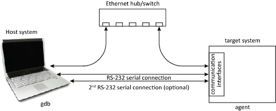
Figure 2.20. Redirected debugging with gdb. For a color version of this figure, see www.iste.co.uk/darche/microprocessor5.zip
ARMulator is an ISA (Instruction Set Architecture) simulator for the ARM® family. It also enables communication with the target so it can be observed. One example of free software is SkyEye.
2.2.7. Summary
A development system is made up of a set of software, hardware and hybrid tools. These include the tools in the development chain (assembler, compiler, link editor10, loader), software and hardware debuggers, the emulator and the logic analyzer.
Table 2.5 shows early examples of debugging. Postmortem debugging consists of stopping the MPU and dumping its main memory (RAM) to analyze its contents. The iterative development method for firmware, called burn and learn programming, consists of writing new firmware, writing it to system ROM in test mode and observing the system as it runs. From this observation, particularly during a crash, the developer can analyze the errors to understand and correct problems.
Table 2.5. Comparison of functionality between various debugging tools (1/2)
| Debugging techniques | ||||
|---|---|---|---|---|
| Characteristics | Postmortem | Burn and learn | Debug monitor (ROM) | Software simulation |
| Real-time execution | Yes | Yes | No | No |
| Software aspects | Memory dump | - | Firmware | Specialized software |
| Hardware aspects | None | None | Possible keyboard/displays | None |
| I/O management | No | No | Yes, but limited | No, to be limited |
| Intrusive | No | No | Yes runs in user space communication interface of the target in use | No |
| Code download | No | No | Yes | Yes |
| Execution commands(run/stop/step) | No | No | Yes | Yes |
| Code breakpoint | No | No | Simple only (generally patched software) | Unlimited, complex |
| Data breakpoint | No | No | No | Yes |
| Complex breakpoint | No | No | No | Yes |
| Access to processor registers/variables | No | No | Yes | Yes |
| On-the-fly access | No | No | No | Yes |
| Watchpoint | No | No | No | Yes |
| Tracing | No | No | No | No |
| Timer | No | No | Can be used in step-by-step monitoring mode | No |
| Wait and stop modes | No | No | Monitoring not accessible in these two modes mode | No |
| Connection (i.e. cabling) | No | No | Simple | No |
| Communications | No | No | RS-232 protocol standard PC data rates | No |
| Loss of processor pin | No | No | No | No |
| Cost | Low | Low | Low | Low |
| Advantages | Simplicity/cost | Simplicity/cost | Simplicity/cost/widespread family support | Simplicity/cost |
| Disadvantages | Very limited functionality | Very limited functionality | Only basic debugging functionality Requires a target with resources (memory, communications) | Real-time aspects are impossible |
Table 2.6 shows more advanced tools. These include in-circuit simulation, in-circuit emulation and in-circuit debugging.
Table 2.6. Comparison of functionality between various debugging tools (2/2)
| Debugging techniques | |||
|---|---|---|---|
| Characteristics | In-circuit simulation (ICS) | In-circuit emulation (ICE) | OCD |
| Real-time execution | No | Yes | Yes |
| Software aspects | Specialized software | Specialized software | Specialized software |
| Hardware aspects | Processor identical to the target | External module with probe | External module |
| I/O management | Yes but limited | Yes | Yes |
| Intrusive | No | No | No |
| Code download | Yes | Yes | Yes |
| Execution commands (run/stop/step) | Yes | Yes | Yes |
| Code breakpoint | Complex (hardware type), unlimited | Complex (hardware type), unlimited | Optional, complex (hardware type), limited |
| Data breakpoint | Yes | Yes | Yes, optional |
| Complex breakpoint | Yes | Yes | Yes |
| Access to processor registers/variables | Yes | Yes | Yes |
| On-the-fly access | Yes | Yes, optional | Yes, optional |
| Watchpoint | Yes | Yes | Yes, optional |
| Tracing | No, to be limited | Yes – real-time | Yes – real-time, optional |
| Timer | No | No | No |
| Wait and stop modes | No | Yes | No |
| Connection (i.e. cabling) | Complex | Complex | Simple |
| Communications | Serial protocol | Dedicated protocol | Dedicated serial protocol |
| Loss of processor pin | No | No | Yes |
| Cost | Low | High | Low, medium if tracing |
| Advantages | Simplicity/cost | Covers all debugging needs | Excellent quality/price ratio |
| Disadvantages | Specific to a family of components Real-time aspects are impossible | High cost Specific hardware to a component Operating frequency limited | Dedicated internal logic Additional interface at the component I/O level |
Chen et al. (2002) categorize modern in-circuit debugging (circa 2000) into two functional modes: ForeGround Debug Mode (F(G)DM) and BackGround Debug Mode (B(G)DM. In the former, the debugger controls the processor’s operation as would an external emulator. In the latter, the microprocessor executes the application until a known event such as a breakpoint is reached, for example. The debugger then transitions to foreground execution; after debugging operations and on command, it returns to the background. Moreover, there are three approaches to debugging: hardware, software and hybrid. The authors have summarized these approaches in Table 2.7. There are completely software-based solutions (approach no. 1, cf. § 2.2.4) and completely hardware-based solutions (approach no. 2 cf. § 2.2.3), as well as two hybrid solutions. Kao et al. (2008) revisited the topic to modify debugging for the SoC environment. For this situation, there are three kinds of architecture: centralized, distributed and hierarchical (Huang and Kao 2000).
Table 2.7. Classification of debugging approaches (Chen et al. 2002). F: Foreground, B: Background, S: Software, H: Hardware
| Approaches | Software emulation (FSBS) | Hardware emulation (FHBH) | Hybrid emulations | ||
| No. | 1 | 2 | 3 | 4 | |
| Modes of operation | Foreground (FDM) | Software | Hardware | Software | Hardware |
| Background(BDM) | Software | Hardware | Hardware | Software | |
| Advantages | Flexible, easy to modify | Complex breakpoint real-time breakpoint execution | Complex breakpoint real-time execution (= FHBH) Flexibility of FDM implementation | Flexibility Easy to modify (= FSBS) Software size for FDM smaller | |
| Disadvantages | System memory space occupied firmware on target (monitor) Longer time to detect breakpoint and to return to user mode | Large number of management logic ports dedicated, unmodifiable solution, inflexible and expensive | Slower FDM execution | Hardware solution is more expensive than FSBS | |
| Examples | Buffalo monitor (Motorola HC11) monitor mode (Motorola HC08) instruction breakpoint and step-by-step mode for x86 | Hardware emulator (ICE) ARM7TDMI | x86 IA-32/64 architecture debugging registers (Intel) | BDM interface (Motorola) core with BSC cells and JTG interface associated with software interrupt instruction | |
2.3. Testing
A microprocessor is, at the very least, a complex VLSI (Very Large-Scale Integration)-type integrated circuit and is therefore difficult to test. This challenge must be overcome when life is on the line, which is the case in the military or space sectors. Aside from those conducted during design, tests were at first done at each manufacturing step, then during the component’s burn-in or stress tests. To facilitate this process, or even to make it possible, the concept of Design for Testability (DfT) has been employed. Testing covers embedded memory (RAM and ROM), including internal data and instruction caches, and other much more limited memory areas such as registers (cf. § V3-3.1), First In, First Out buffers (FIFO, this will be covered in a future books by the author on memories and storage), etc. In § 2.2.5, we presented the IEEE 1149.1 standard, an access method belonging to the DfT approach and based on a test path (access or scan) that enables access to the logic circuit’s internal nodes, with testing carried out using an external device. Manufacturers of advanced microprocessors now integrate internal self-test logic (BIST for Built-In Self-Test, Agrawal et al. (1993a, 1993b) and cf. § 3.9 in Darche (2004), which makes it possible to determine if the circuit is functioning correctly. For more information on this broad subject, see Wang et al. (2006) and Navabi (2010).
Errors during execution of an instruction can be caused by misuse, a component design bug or an unreferenced instruction. An example of the first case is division by zero. For the second, consider the fdiv floating-point division bug in the Intel Pentium® 5 discovered in 1994. An unreferenced instruction is an instruction code that is not documented in the official documentation. In the best case, it has no effect (equivalent to a nop). In the worst case, it creates a temporal reliability problem in programs that use it. For example, there were hidden instructions in MOS Technology’s MCSD6502 MPU.
2.4. Conclusion
We have described the software development chain for a microprocessor system application. Software and hardware debugging tools were shown. Early debugging tools and practices such as postmortem analysis and the iterative burn and learn approach are no longer suitable today. Increasingly complex and fast MPUs require integration of testing and debugging logic as close to the core as possible. Internal debugging (OCD) and associated communication interfaces such as the JTAG interface were then examined. To conclude, we presented an overview of assembly language. This language enables symbolic manipulation of instructions, data (variables and constants) and addresses. High-Level (programming) Languages (HLL) have taken their place in embedded systems thanks to progress in storage and compilers. But it is still used in specific circumstances such as to optimize memory use and execution time, for system or hardware interfacing, or for teaching computer architecture. To learn more about this language for a specific processor, Streib (2011) presents an example from the Intel world.
The next chapter shows the microprocessor in the earliest hardware environments that were widely distributed, namely microcomputers.
- 1 Controller associated with this interface: UART, for Universal Asynchronous Receiver Transmitter. Today, this interface is emulated via a USB interface.
- 2 Real-time debugging is outside the scope of this work and will not be addressed.
- 3 In terms of the Boolean algebra (i.e. alternating between 0 and 1).
- 4 MCU for MicroController Unit or μC, cf. § V3-5.3.
- 5 The acronym ICD (In-Circuit Debugger) is rarely used. It is more specifically used in the commercial domain.
- 6 The use of registers DR4 and DR5 is reserved by Intel.
- 7 Except for three analog signals, XTAL, EXTAL and XFC.
- 8 Term derived from the Flash EEPROM memory technology.
- 9 GNU for GNU’s Not UNIX.
- 10 That is, a linker.