
6
Subsystem Design
Highlights: |
Pipelines and data paths. |
Adders. |
Multipliers. |
Memory. |
PLAs. |
6.1 Introduction
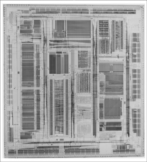
Most chips are built from a collection of subsystems: adders, register files, state machines, etc. Of course, to do a good job of designing a chip, we must be able to properly design each of the major components. Studying individual subsystems is also a useful prelude to the study of complete chips because a single component is a focused design problem. When designing a complete chip, such as the HP 7200 CPU shown in Figure 6-1, we often have to perform several different types of computation, each with different cost constraints. A single component, on the other hand, performs a single task; as a result, the design choices are much more clear.
Figure 6-1: The HP 7200 CPU. (© Copyright 1996 Hewlett-Packard Company. Reproduced with permission.)
As always, the cost of a design is measured in area, delay, and power. For most components, we have a family of designs that all perform the same basic function, but with different area/delay trade-offs. Having access to a variety of ways to implement a function gives us architectural freedom during chip design. Area and delay costs can be reduced by optimization at each level of abstraction:
• Layout. We can make microscopic changes to the layout to reduce parasitics: moving wires to pack the layout or to reduce source/drain capacitance, adding vias to reduce resistance, etc. We can also make macroscopic changes by changing the placement of gates, which may reduce wire parasitics, reduce routing congestion, or both.
• Circuit. Transistor sizing is the first line of defense against circuits that inherently require long wires. Advanced logic circuits, such as precharged gates, may help reduce the delay within logic gates.
• Logic. As we saw in Chapter 3, redesigning the logic to reduce the gate depth from input to output can greatly reduce delay, though usually at the cost of area.
• Register-transfer and above. Proper placement of memory elements makes maximum use of the available clock period. Proper encoding of signals allows clever logic designs that minimize logic delay. Pipelining provides trade-offs between clock period and latency.
While it may be tempting to optimize a design by hacking on the layout, that is actually the least effective way to achieve your desired area/delay design point. If you choose to make a circuit faster by tweaking the layout and you fail, all that layout work must be thrown out when you try a new circuit or logic design. On the other hand, changing the register-transfer design does not preclude further work to fine-tune area or performance. The gains you can achieve by modifications within a level of abstraction grow as you move up the abstraction hierarchy: layout modifications typically give 10%–20% performance improvement; logic redesign can cut delay by more than 20%; we will see how the register-transfer modifications that transform a standard multiplier into a Booth multiplier can cut the multiplier’s delay in half. Furthermore, layout improvements take the most work—speeding up a circuit usually requires modifying many rectangles, while the architecture can be easily changed by redrawing the block diagram. You are best off pursuing the largest gains first, at the highest levels of abstraction, and doing fine-tuning at lower levels of abstraction only when necessary.
Logic and circuit design are at the core of subsystem design. Many important components, foremost being the adder, have been so extensively studied that specific optimizations and trade-offs are well understood. However, there are some general principles which can be applied to subsystems. We will first survey some important design concepts, then delve into the details of several common types of subsystem-level components.
6.2 Subsystem Design Principles
6.2.1 Pipelining
Pipelining is a relatively simple method for reducing the clock period of long combinational operations. Complex combinational components can pose serious constraints on system design if their delay is much longer than the delay of the other components. If the propagation time through that combinational element determines the clock period, logic in the rest of the chip may sit idle for most of the clock cycle while the critical element finishes. Pipelining allows large combinational functions to be broken up into pieces whose delays are in balance with the rest of the system components.
Figure 6-2: Structure of a pipelined system.

As illustrated in Figure 6-2, pipelining entails introducing a rank of memory elements along a cut through the combinational logic. We usually want all the outputs to appear on the same clock cycle, which implies that the cut must divide the inputs and outputs into disjoint sets. The pipelined system still computes the same combinational function but that function requires several cycles to be computed.
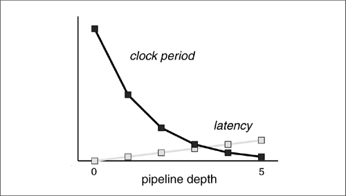
The number of cycles between the presentation of an input value and the appearance of its associated output is the latency of the pipeline. Figure 6-3 shows how clock period and latency vary with the number of stages in a pipeline. Moderate amounts of pipelining cause a great reduction in clock period, but heavy pipelining provides only modest, and decreasing gains. Meanwhile, latency increases linearly. The total delay through the pipelined system is slightly longer than the combinational delay thanks to the setup and hold requirements of the memory elements. But the clock period can be substantially reduced by pipelining, balancing the pipelined system’s critical delay path lengths with those in the rest of the system.
Figure 6-3: Clock period and latency as a function of pipeline depth.
When pipelining, memory elements can be placed along any cut, the best placement balances delays through the combinational logic. As shown in Figure 6-4, if memory elements are placed so that some delay paths are much longer than others, you have recreated in miniature the same conditions that caused you to pipeline the logic in the first place. Perfect pipelining balances the delays between ranks of memory elements, using the principles described in Section 5.4.
Figure 6-4: A pipeline with unbalanced stage delays.

6.2.2 Data Paths
A data path is both a logical and a physical structure: it is built from components which perform typical data operations, such as addition and it has a layout structure which takes advantage of the regular logical design of the data operators. Data paths typically include several types of components: registers (memory elements) store data; adders and ALUs perform arithmetic; shifters perform bit operations; counters may be used for program counters. A data path may include point-to-point connections between pairs of components, but the typical data path has too many connections for every component to be connected to every other component. Data is often passed between components on one or more busses, or common connections; the number of busses determines the maximum number of data transfers on a clock cycle and is a primary design parameter of data paths.
Figure 6-5: Structure of a typical bit-slice data path.

Most data operations are regular—we saw in the previous sections that adders, ALUs, shifters, and other operators can be constructed from arrays of smaller components. The cleanest way to take advantage of this regularity in most cases is to design the layout as a bit-slice, as shown in Figure 6-5. A bit-slice, as the name implies, is a one-bit version of the complete data path, and the n-bit data path is constructed by replicating the bit-slice. Typically, data flows horizontally through the bit-slice along point-to-point connections or busses, while control signals (which provide read and write signals to registers, opcodes for ALUs, etc.) flow vertically.
Bit-slice layout design requires careful, simultaneous design of the cells that comprise the data path. Since the bit-slice must be stacked vertically, any signals that pass through the cells must be tilable—the signals must be aligned at top and bottom. Horizontal constraints are often harder to satisfy. The VDD and VSS lines must run horizontally through the cells, as must busses. Signals between adjacent cells must also be aligned. While the vertical wires usually distribute signals, the horizontal wires are often interrupted by logic gates. The transistors in the cells impose constraints on the layout that may make it hard to place horizontal connections at the required positions. As shown in Figure 6-6, cells often need to be stretched beyond their natural heights to make connections with other cells.
Figure 6-6: Abutting cells may require moving pins or stretching.

Figure 6-7: A simple wiring plan.

The data path’s layout design also requires careful consideration of layer assignments. With a process that provides two levels of metal, metal 1 is typically used for horizontal wires and metal 2 for vertical wires. A wiring plan helps organize your thoughts on the wires required, their positions, and the best layers to use for each wire. A black-and-white wiring plan is shown in Figure 6-7; you should draw your wiring plans in color to emphasize layer choices.
Two circuit design problems unique to data path design are registers and busses. The circuit chosen for the register depends on the number of registers required. If only a few registers are needed, a standard latch or flip-flop from Section 5.2 is a perfectly reasonable choice. If many registers are required, area can be saved by using an n-port static RAM, which includes one row enable and one pair of bit lines for each port. Although an individual bit/word can allow only one read or write operation at a time, the RAM array can support the simultaneous, independent reading or writing of two words simply by setting the select lines of the two words high at the same time. One SRAM port is required for each bus in the data path.
A bit-slice with connections between all pairs of components would be much too large: not only would it be much too tall because of the large number of horizontal wires needed for the connections, but it would also be made longer by the many signals required to control the connections. Data paths are almost always made with busses that provide fewer connections at much less cost in area. Since the system probably doesn’t need all data path components to talk to each other simultaneously, connections can be shared. But these shared connections often require special circuits that take up a small amount of space while providing adequate speed of communication. While a multiplexer provides the logical function required to control access to the bus, a mux built from static complementary gates would be much too large.
Figure 6-8: A pseudo-nMOS bus circuit.

A more clever circuit design for a bus is as a distributed NOR gate: the common wire forms the NOR gate’s output, while pulldowns at the sources select the source and set the NOR gate’s output. (All devices connected to the bus can read it in this scheme.) The circuit choices for busses are much like those for the advanced gate circuits of Section 3.5: pseudo-nMOS, shown in Figure 6-8, and precharged, shown in Figure 6-9. The trade-offs are also similar: the pseudo-nMOS bus is slow but does not require a separate precharge phase.
Figure 6-9: A precharged bus circuit.

6.3 Combinational Shifters
A shifter is most useful for arithmetic operations since shifting is equivalent to multiplication by powers of two. Shifting is necessary, for example, during floating-point arithmetic. The simplest shifter is the shift register, which can shift by one position per clock cycle. However, that machine isn’t very useful for most arithmetic operations—we generally need to shift several bits in one cycle and to vary the length of the shifts.
Figure 6-10: How a barrel shifter performs shifts and rotates.
A barrel shifter [Mea80] can perform n-bit shifts in a single combinational function, and it has a very efficient layout. It can rotate and extend signs as well. Its architecture is shown in Figure 6-10. The barrel shifter accepts 2n data bits and n control signals and produces n output bits. It shifts by transmitting an n-bit slice of the 2n data bits to the outputs. The position of the transmitted slice is determined by the control bits; the exact operation is determined by the values placed at the data inputs. Consider two examples:
• Send a data word d into the top input and a word of all zeroes into the bottom input. The output is a right shift (imagine standing at the output looking into the barrel shifter) with zero fill. Setting the control bits to select the top-most n bits is a shift of zero, while selecting the bottom-most n bits is an n-bit shift that pushes the entire word out of the shifter. We can shift with a ones fill by sending an all-ones word to the bottom input.
• Send the same data word into both the top and bottom inputs. The result is a rotate operation—shifting out the top bits of a word causes those bits to reappear at the bottom of the output.
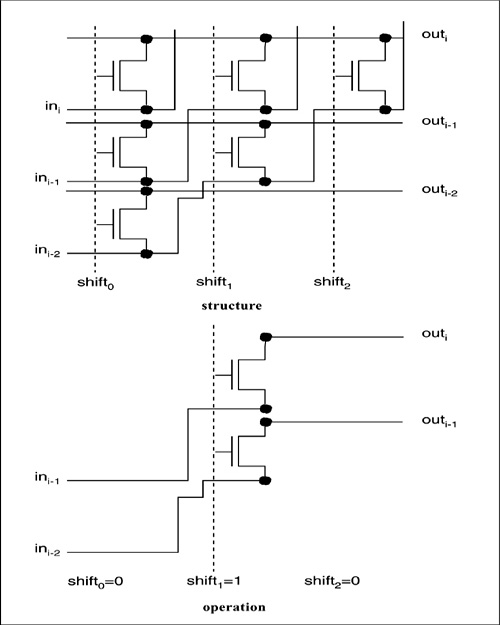
How can we build a circuit that can select an arbitrary n bits and how do we do it in a reasonably sized layout? A barrel shifter with n output bits is built from a 2n vertical by n horizontal array of cells, each of which has a single transistor and a few wires. The schematic for a small group of contiguous cells is shown in Figure 6-11. The core of the cell is a transmission gate built from a single n-type transistor; a complementary transmission gate would require too much area for the tubs. The control lines run vertically; the input data run diagonally upward through the system; the output data run horizontally. The control line values are set so that exactly one is 1, which turns on all the transmission gates in a single column. The transmission gates connect the diagonal input wires to the horizontal output wires; when a column is turned on, all the inputs are shunted to the outputs. The length of the shift is determined by the position of the selected column—the farther to the right it is, the greater the distance the input bits have travelled upward before being shunted to the output.
Note that, while this circuit has many transmission gates, each signal must traverse only one transmission gate. The delay cost of the barrel shifter is largely determined by the parasitic capacitances on the wires, which is the reason for squeezing the size of the basic cell as much as possible. In this case, area and delay savings go hand-in-hand.
Figure 6-11: A section of the barrel shifter.
6.4 Adders
The adder is probably the most studied digital circuit. There are a great many ways to perform binary addition, each with its own area/delay trade-offs. A great many tricks have been used to speed up addition: encoding, replication of common factors, and precharging are just some of them. The origins of some of these methods are lost in the mists of antiquity. Since advanced circuits are used in conjunction with advanced logic, we need to study some higher-level addition methods before covering circuits for addition.
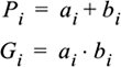
The basic adder is known as a full adder. It computes a one-bit sum and carry from two addends and a carry-in. The equations for the full adder’s functions are simple:
(EQ 6-1)

In these formulas, si is the sum at the ith stage and ci+1 is the carry out of the ith stage.
The n-bit adder built from n one-bit full adders is known as a ripple-carry adder because of the way the carry is computed. The addition is not complete until the n-1th adder has computed its sn-1 output; that result depends on ci input, and so on down the line, so the critical delay path goes from the 0-bit inputs up through the ci’s to the n-1 bit. (We can find the critical path through the n-bit adder without knowing the exact logic in the full adder because the delay through the n-bit carry chain is so much longer than the delay from a and b to s.) The ripple-carry adder is area efficient and easy to design but is slow when n is large.
Speeding up the adder requires speeding up the carry chain. The carry-lookahead adder is one way to speed up the carry computation. The carry-lookahead adder breaks the carry computation into two steps, starting with the computation of two intermediate values. The adder inputs are once again the ai’s and bi’s; from these inputs, P (propagate) and G (generate) are computed:
(EQ 6-2)
If Gi = 1, there is definitely a carry out of the ith bit of the sum—a carry is generated.
If Pi = 1, then the carry from the i-1th bit is propagated to the next bit. The sum and carry equation for the full adder can be rewritten in terms of P and G:
(EQ 6-3)
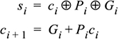
The carry formula is smaller when written in terms of P and G, and therefore easier to recursively expand:
(EQ 6-4)
The ci+1 formula of Equation 6-4 depends on ci-2, but not ci or ci-1. After rewriting the formula to eliminate ci and ci-1, we used the speedup trick of Section 4.4—we eliminated parentheses, which substitutes larger gates for long chains of gates. There is a limit beyond which the larger gates are slower than chains of smaller gates; typically, four levels of carry can be usefully expanded.
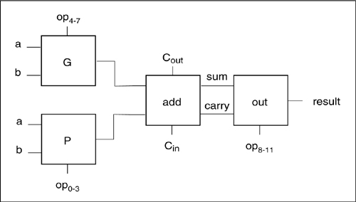
A depth-4 carry-lookahead unit is shown in Figure 6-12. The unit takes the P and G values from its four associated adders and computes four carry values. Each carry output is computed by its own logic. The logic for ci+3 is slower than that for ci, but the flattened ci+3 logic is faster than the equivalent ripple-carry logic.
There are two ways to hook together depth-b carry-lookahead units to build an n-bit adder. The carry-lookahead units can be recursively connected to form a tree: each unit generates its own P and G values, which are used to feed the carry-lookahead unit at the next level of the tree. A simpler scheme is to connect the carry-ins and carry-outs of the units in a ripple chain. This approach is most common in chip design because the wiring for the carry-lookahead tree is hard to design and area-consuming.
The carry-skip adder [Leh61] looks for cases in which the carry out of a set of bits is the same as the carry in to those bits. This adder makes a different use of the carry-propagate relationship. A carry-skip adder is typically organized into m-bit groups; if the carry is propagated for every bit in the stage, then a bypass gate sends the stage’s carry input directly to the carry output. The structure of the carry chain for acarry-skip adder divided into groups of bits is shown in Figure 6-13. A true carry into the group and true propagate condition P at every bit in the group is needed to cause the carry to skip. It is possible to determine the optimum number of bits in a group [Kor93]. The worst case for the carry signal occurs when there is a carry propagated through every bit, but in this case Pi will be true at every bit. Therefore, the longest path for the carry begins when the carry is generated at the bottom bit of the bottom group (rippling through the remainder of the group), is skipped past the intermediate groups, and ripples through the last group; the carry must necessity ripple through the first and last groups to compute the sum. Using some simple assumptions about the relative delays for a ripple through a group and skip, Koren estimates the optimum group size for an n-bit word as
Figure 6-12: Structure of a carry lookahead adder.

Figure 6-13: The carry-select adder.

(EQ 6-5)
![]()
Since the carry must ripple through the first and last stages, the adder can be further speeded up by making the first and last groups shorter than this length and by lengthening the middle groups.
The carry-select adder computes two versions of the addition with different carry-ins, then selects the right one. Its structure is shown in Figure 6-13. As with the carry-skip adder, the carry-select adder is typically divided into m-bit stages. The second stage computes two values: one assuming that the carry-in is 0 and another assuming that it is 1. Each of these candidate results can be computed by your favorite adder structure. The carry-out of the previous stage is used to select which version is correct: multiplexers controlled by the previous stage’s carry-out choose the correct sum and carry-out. This scheme speeds up the addition because the ith stage can be computing the two versions of the sum in parallel with the i-1th’s computation of its carry. Once the carry-out is available, the ith stage’s delay is limited to that of a two-input multiplexer.
No matter what style of circuit is used for the carry chain, we can size transistors to reduce the carry chain delay. By increasing widths of transistors on critical delay paths, we can steadily reduce the carry delay to the ring oscillator limit [Fis92]. In a carry-lookahead adder, the carry-in signal is of medium complexity; depending on the exact logic implementation, either P or G will be most critical, with the other signal being less critical than carry-in. At the adder’s high-order bits, the non-carry outputs of the carry chain also become critical, requiring larger transistors; otherwise, the stages of an optimally-sized adder are identical.
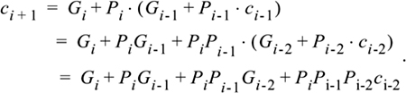
Precharged circuits are an obvious way to speed up the carry chain. One of the most interesting precharged adders is the Manchester carry chain [Mea80], which computes the sum from P and G. Two bits of a Manchester carry chain are shown in Figure 6-14. The storage node, which holds the complement of the carry (ci’), is charged to 1 during the precharge phase. If Gi = 1 during the evaluate phase, the storage node is discharged, producing a carry into the next stage. If Pi = 1, then the ith storage node is connected to the i-1th storage node; in this case, the ith storage node can be discharged by the Pi-1 pulldown or, if the Ci-1 transmission gate is on, by a preceding P pulldown. In the worst case, the n-1th storage node will be discharged through the 0th pulldown and through n transmission gates, but in the typical case, the pulldown path for a storage node is much shorter. The widest transistors should be at the least-significant bit stage since they see the largest load. The next example describes the use of a Manchester carry chain in a high-performance microprocessor.
Figure 6-14: A Manchester carry chain.

Example 6-1: Carry chain of the DEC Alpha 21064 microprocessor
The first DEC Alpha microprocessor, the 21064, used a Manchester carry chain [Dob92]. That processor had a 64-bit word with the carry chain organized into groups of 8 bits to enable byte-wise operation. The carry circuit at each stage was made entirely of n-type devices:
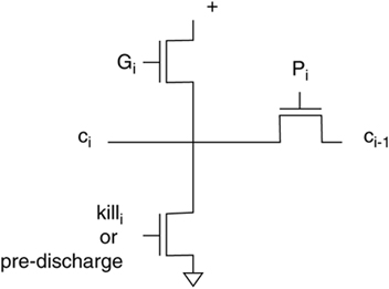
The carry chain uses carry propagate, generate, and kill signals. The chain is pre-discharged and then selectively charged using the n-type pullups. Pre-discharging was used to avoid the threshold drop on the carry signal introduced by precharging through an n-type device; precharging to VDD-Vt was deemed to provide unacceptable noise margins. The pass transistors for the carry were sized with the largest transistors at the least-significant bit.
Each group of eight bits was organized into a 32-bit carry-select, and a logarithmic carry-select technique was used to generate the 64-bit sum. As a result, there were two carry chains in each 8-bit group: one for the zero-carry-in case and another for the one-carry-in case.
Serial adders present an entirely different approach to high-speed arithmetic—they require many clock cycles to add two n-bit numbers, but with a very short cycle time. Serial adders can work on nybbles (4-bit words) or bytes, but the bit-serial adder [Den85], shown in Figure 6-15 is the most extreme form. The data stream consists of three signals: the two numbers to be added and an LSB signal that is high when the current data bits are the least significant bits of the addends. The addends appear LSB first and can be of arbitrary length—the end of a pair of numbers is signaled by the LSB bit for the next pair. The adder itself is simply a full adder with a memory element for the carry. The LSB signal clears the carry register. Subsequently, the two input bits are added with the carry-out of the last bit. The serial adder is small and has a cycle time equal to that of a single full adder.
Figure 6-15: A bit-serial adder.

Table 6-1: Average power consumption of 16-bit adders calculated from circuit simulation. (After Callahan and Schwartzlander. Copyright © 1996 Kluwer Academic Publishers. Used with permission.)

Callaway and Schwartzlander [Cal96] evaluated the power consumption of several types of parallel adders. Their results from circuit simulation of 16-bit adders are summarized in Table 6-1. In general, slower adders consume less power. The exception is the carry-skip adder, which uses less current than the ripple-carry adder because, although it consumes a higher peak current, the current falls to zero very quickly. They measured the average power consumption of fabricated circuits and showed that these estimates were well-correlated with the behavior of actual circuits.
6.5 ALUs
The arithmetic logic unit, or ALU, is a modified adder. While an ALU can perform both arithmetic and bit-wise logical operations, the arithmetic operations’ requirements dominate the design.
A basic ALU takes two data inputs and a set of control signals, also called an opcode. The opcode, together with the ALU’s carry-in, determine the ALU’s function. For example, if the ALU is set to add, then c0 = 0 produces a+b while c0 = 1 produces a+b+1.
Figure 6-16: A three function block ALU.
The logic to compute all possible ALU functions can be large unless it is carefully designed. The ALU presents an ideal opportunity to use transmission gate logic by building a three function block ALU [Mea80], shown in Figure 6-16. The function block is shown in Figure 6-17; it takes two data inputs and their complements along with four control signals and can compute all 16 possible functions of the two data inputs.
Figure 6-17: A two-input function block.

The ALU is built around an adder. The three function blocks require a total of 12 opcode bits to determine the ALU’s function. The two function blocks at the inputs compute signals used to drive the adder’s P and G inputs, but those signals are not necessarily the propagate and generate functions defined for carry-lookahead addition—they are signals required to drive the adder block to compute the required values. The ALU’s output is computed by the final function block from the adder’s carry and the propagate signal.
Not all ALUs must implement the full set of logical functions. If the ALU need implement only a few functions, the function block scheme may be overkill. An ALU which, for example, must implement only addition, subtraction, and one or two bit-wise functions can usually be implemented using static gates.
6.6 Multipliers
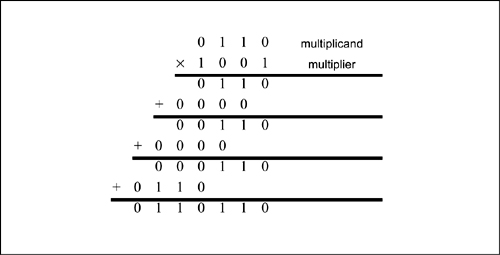
Multiplier design starts with the elementary school algorithm for multiplication. Consider the simple example of Figure 6-18. At each step, we multiply one digit of the multiplier by the full multiplicand; we add the result, shifted by the proper number of bits, to the partial product. When we run out of multiplier digits, we are done. Single-digit multiplication is easy for binary numbers—binary multiplication of two bits is performed by the AND function. The computation of partial products and their accumulation into the complete product can be optimized in many ways, but an understanding of the basic steps in multiplication is important to a full appreciation of those improvements.
Figure 6-18: Multiplication using the elementary school algorithm.
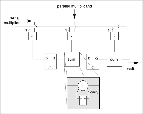
One simple, small way to implement the basic multiplication algorithm is the serial-parallel multiplier of Figure 6-19, so called because the n-bit multiplier is fed in serially while the m-bit multiplicand is held in parallel during the course of the multiplication. The multiplier is fed in least-significant bit first and is followed by at least m zeroes. The result appears serially at the end of the multiplier chain. A one-bit multiplier is simply an AND gate. The sum units in the multiplier include a combinational full adder and a register to hold the carry. The chain of summation units and registers performs the shift-and-add operation—the partial product is held in the shift register chain, while the multiplicand is successively added into the partial product.
One important complication in the development of efficient multiplier implementations is the multiplication of two’s-complement signed numbers. The Baugh-Wooley multiplier [Bau73] is the best-known algorithm for signed multiplication because it maximizes the regularity of the multiplier logic and allows all the partial products to have positive sign bits. The multiplier X can be written in binary as
Figure 6-19: Basic structure of a serial-parallel multiplier.
(EQ 6-6)

where n is the number of bits in the representation. The multiplicand Y can be written similarly. The product P can be written as
(EQ 6-7)

When this formula is expanded to show the partial products, it can be seen that some of the partial products have negative signs:

The formula can be further rewritten, however, to move the negative-signed partial products to the last steps and to add the negation of the partial product rather than subtract. Further rewriting gives this final form:
(EQ 6-9)

Each partial product is formed with AND functions and the partial products are all added together. The result is to push the irregularities to the end of the multiplication process and allow the early steps in the multiplication to be performed by identical stages of logic.
The elementary school multiplication algorithm (and the Baugh-Wooley variations for signed multiplication) suggest a logic and layout structure for a multiplier which is surprisingly well-suited to VLSI implementation—the array multiplier. The structure of an array multiplier for unsigned numbers is shown in Figure 6-20. The logic structure is shown in parallelogram form both to simplify the drawing of wires between stages and also to emphasize the relationship between the array and the basic multiplication steps shown in Figure 6-18. As when multiplying by hand, partial products are formed in rows and accumulated in columns, with partial products shifted by the appropriate amount. In layout, however, the y bits generally would be distributed with horizontal wires since each row uses exactly one y bit.
Notice that only the last adder in the array multiplier has a carry chain. The earlier additions are performed by full adders which are used to reduce three one-bit inputs to two one-bit outputs. Only in the last stage are all the values accumulated with carries. As a result, relatively simple adders can be used for the early stages, with a faster (and presumably larger and more power-hungry) adder reserved for the last stage. As a result, the critical delay path for the array multiplier follows the trajectory shown in Figure 6-21.
Figure 6-20: Structure of an unsigned array multiplier.

Figure 6-21: The critical delay path in the array multiplier.

Pipelining reduces cycle time but doesn’t reduce the total time required for multiplication. One way to speed up multiplication is Booth encoding [Boo51], which performs several steps of the multiplication at once. Booth’s algorithm takes advantage of the fact that an adder-subtractor is nearly as fast and small as a simple adder. In the elementary school algorithm, we shift the multiplicand x, then use one bit of the multiplier y if that shifted value is to be added into the partial product. The most common form of Booth’s algorithm looks at three bits of the multiplier at a time to perform two stages of the multiplication.
Consider once again the two’s-complement representation of the multiplier y:
(EQ 6-10)
![]()
We can take advantage of the fact that 2a = 2a+1-2a to rewrite this as
(EQ 6-11)
![]()
Now, extract the first two terms:
![]()
Each term contributes to one step of the elementary-school algorithm: the right-hand term can be used to add x to the partial product, while the left-hand term can add 2x. (In fact, since yn-2 also appears in another term, no pair of terms exactly corresponds to a step in the elementary school algorithm. But, if we assume that the y bits to the right of the decimal point are 0, all the required terms are included in the multiplication.) If, for example, yn-1 = yn, the left-hand term does not contribute to the partial product. By picking three bits of y at a time, we can determine whether to add or subtract x or 2x (shifted by the proper amount, two bits per step) to the partial product. Each three-bit value overlaps with its neighbors by one bit. Table 6-2 shows the contributing term for each three-bit code from y.
Table 6-2 Action s during Booth multiplication.

Let’s try an example to see how this works: x = 011001 (2510), y = 101110 (-1810). Call the ith partial product Pi. At the start, P0 = 00000000000 (two six-bit numbers give an 11-bit result):
1. y1y0y-1 = 100, so P1 = P0-(10.011001) - 11111001110.
2. y3y2y1 = 111, so P2 = P1 + 0 = 11111001110.
3. y5y4y3 = 101, so P3 = P2-0110010000 = 11000111110.
In decimal, y1y0y-1 contribute - 2x·1, y3y2y1 contribute 0·4, and y5y4y3 contribute - x·16, giving a total of - 18x. Since the multiplier is - 18, the result is correct.
Figure 6-22: Structure of a Booth multiplier.
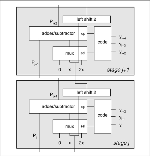
Figure 6-22 shows the detailed structure of a Booth multiplier. The multiplier bits control a multiplexer which determines what is added to or subtracted from the partial product. Booth’s algorithm can be implemented in an array multiplier since the accumulation of partial products still forms the basic trapezoidal structure. In this case, a column of control bit generators on one side of the array analyzes the triplets of y bits to determine the operation in that row.
Another way to speed up multiplication is to use more adders to speed the accumulation of partial products. The best-known method for speeding up the accumulation is the Wallace tree [Wal64], which is an adder tree built from carry-save adders, which is simply an array of full adders whose carry signals are not connected, as in the early stages of the array multiplier. A carry save adder, given three n-bit numbers a, b, c, computes two new numbers y, z such that y + z = a + b + c. The Wallace tree performs the three-to-two reductions; at each level of the tree, i numbers are combined to form ![]() 2i/3
2i/3 ![]() sums. When only two values are left, they are added with a high-speed adder. Figure 6-23 shows the structure of a Wallace tree. The partial products are introduced at the bottom of the tree. Each of the z outputs is shifted left by one bit since it represents the carry out.
sums. When only two values are left, they are added with a high-speed adder. Figure 6-23 shows the structure of a Wallace tree. The partial products are introduced at the bottom of the tree. Each of the z outputs is shifted left by one bit since it represents the carry out.
Figure 6-23: Structure of a Wallace tree.

A Wallace tree multiplier is considerably faster than a simple array multiplier because its height is logarithmic in the word size, not linear. However, in addition to the larger number of adders required, the Wallace tree’s wiring is much less regular and more complicated. As a result, Wallace trees are often avoided by designers who do not have extreme demands for multiplication speed and for whom design complexity is a consideration.
Callaway and Schwartzlander [Cal96] also evaluated the power consumption of multipliers. They compared an array multiplier and a Wallace tree multiplier (both without Booth encoding) and found that the Wallace tree multiplier used significantly less power for bit widths between 8 and 32, with the advantage of the Wallace tree growing as word length increased.
6.7 High-Density Memory
So far, we have built memory elements out of circuits that exhibit mostly digital behavior. By taking advantage of analog design methods, we can build memories that are both smaller and faster. Memory design is usually best left to expert circuit designers; however, understanding how these memories work will help you learn how to use them in system design. On-chip memory is becoming increasingly important as levels of integration increase to allow both processors and useful amounts of memory to be integrated on a single chip [Kog95].
Read-only memory (ROM), as the name implies, can be read but not written. It is used to store data or program values that will not change, because it is the densest form of memory available. An increasing number of digital logic processes support flash memory, which is the dominant form of electrically erasable PROM memory. There are two types of read-write random access memories: static (SRAM) and dynamic (DRAM). SRAM and DRAM use different circuits, each of which has its own advantages: SRAM is faster but uses more power and is larger; DRAM has a smaller layout and uses less power. DRAM cells are also somewhat slower and require the dynamically stored values to be periodically refreshed, just as in a dynamic latch.
Some types of memory are available for integration on a chip, while others that require special processes are generally used as separate chips. Commodity DRAMs are based on a one-transistor memory cell. That cell requires specialized structures, such as poly-poly capacitors, which are built using special processing steps not usually included in ASIC processes. A design that requires high-density ROM or RAM is usually partitioned into several chips, using commodity memory parts. Medium density memory, on the order of one K bytes, can often be put on the same chip with the logic that uses it, giving faster access times, as well as greater integration.
Figure 6-24: Architecture of a high-density memory system.
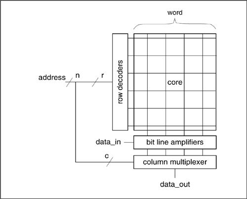
A RAM or ROM is used by presenting it with an address and receiving the value stored at that address some time later. Details differ, of course: large memories often divide the address into row and column sections, which must be sent to the memory separately, for example. The simplest and safest way to use memory in a system is to treat it as a strict sequential component: send the address to the memory on one cycle and read the value on the next cycle.
The architecture of a generic RAM/ROM system is shown in Figure 6-24. Think of the data stored in the memory core as being organized into n bit-wide words. The address decoders (also known as row decoders) translate the binary address into a unary address—exactly one word in the core is selected. A read is performed by having each cell in the selected word set the bit and bit’ lines to the proper values: bit = 1, bit’ = 0 if a 1 is stored in the array, for example. The bit lines are typically precharged, so the cell discharges one of the lines. The bit lines are read by circuits that sense the value on the line, amplify it to speed it up, and restore the signal to the proper voltage levels. A write is performed by setting the bit lines to the desired values and driving that value from the bit lines into the cell. If the core word width is narrower than the final word width (for example, a one-bit wide RAM typically has a core much wider than one bit to make a more compact layout), a multiplexer uses the bottom few bits of the address to select the desired bits out of the word.
The row decoders are not very complex: they typically use NOR gates to decode the address, followed by a chain of buffers to allow the circuit to drive the large capacitance of the word line. There are two major choices for circuits to implement the NOR function: pseudo-nMOS and precharged. Pseudo-nMOS circuits are adequate for small memories, but precharged circuits offer better performance (at the expense of control circuitry) for larger memory arrays. Figure 6-25 shows a precharged row decoder; the true and complement forms of the address lines can be distributed vertically through the decoders and connected to the NOR pulldowns as appropriate for the address to be decoded at that row.
Figure 6-25: A precharged row decoder.

The column decoders are typically implemented as pass transistors on the bit lines. As shown in Figure 6-26, each output bit will be selected from several columns. The multiplexer control signals can be generated at one end of the string of multiplexers and distributed to all the mux cells.
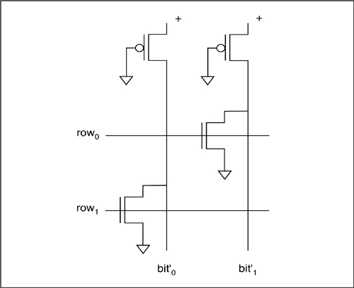
6.7.1 ROM
A read-only memory is programmed with transistors to supply the desired values. A common circuit is the NOR array shown in Figure 6-27. It uses a pseudo-nMOS NOR gate: a transistor is placed at the word-bit line intersection for which bit’ = 0. Programmable ROMs (PROMs) are also available. The simplest PROM uses a high voltage to blow selected fuses in the array; this type of programming cannot be undone.
Figure 6-26: A column decoding scheme.
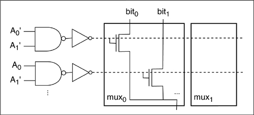
Figure 6-27: Design of a ROM core.
Electrically or UV-erasable ROMs allow the ROM to be erased, then reprogrammed many times. However, both programmable and erasable memories usually require special processing steps which are not often available to the average VLSI designer.
6.7.2 Static RAM
Basic static RAM circuits can be viewed as variations on the designs used for latches and flip-flops; more aggressive static RAMs make use of design tricks originally developed for dynamic RAMs to speed up the system.
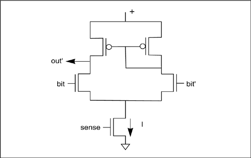
Figure 6-28: Design of an SRAM core cell.
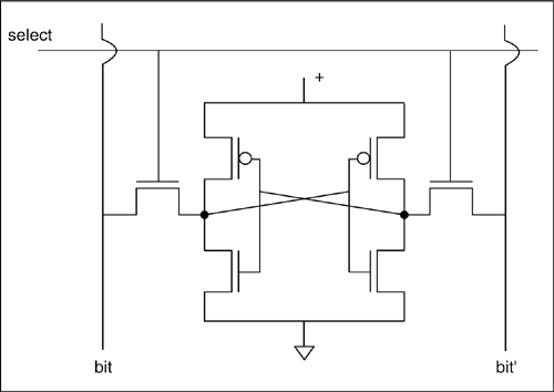
The SRAM core circuit is shown in Figure 6-28. The value is stored in the middle four transistors, which form a pair of inverters connected in a loop (try drawing a gate-level version of this schematic). The other two transistors control access to the memory cell by the bit lines. When select = 0, the inverters reinforce each other to store the value. A read or write is performed when the cell is selected:
• To read, bit and bit’ are precharged to VDD before the select line is allowed to go high. One of the cell’s inverters will have its output at 1, and the other at 0; which inverter is 1 depends on the value stored. If, for example, the right-hand inverter’s output is 0, the bit’ line will be drained to VSS through that inverter’s pulldown and the bit line will remain high. If the opposite value is stored in the cell, the bit line will be pulled low while bit’ remains high.
• To write, the bit and bit’ lines are set to the desired values, then select is set to 1. Charge sharing forces the inverters to switch values, if necessary, to store the desired value. The bit lines have much higher capacitance than the inverters, so the charge on the bit lines is enough to overwhelm the inverter pair and cause it to flip state.
Figure 6-29: A differential pair sense amplifier for an SRAM.
The layout of a pair of SRAM cells in the SCMOS rules is shown in Figure 6-31.
Figure 6-30: An SRAM pre-charge circuit.
A sense amplifier, shown in Figure 6-29, makes a reasonable bit line receiver for modest-size SRAMs. The n-type transistor at the bottom acts as a switchable current source—when turned on by the sense input, the transistor pulls a fixed current I through the sense amp’s two arms. Kirchoff’s current law tells us that the currents through the two branches must sum to I. When one of the bit lines goes low, the current through that leg of the amplifier goes low, increasing the current in the other leg. P-type transistors are used as loads. For an output of the opposite polarity, both the output and the pullup bias connection must be switched to the opposite sides of the circuit. More complex circuits can determine the bit line value more quickly [Gla85].
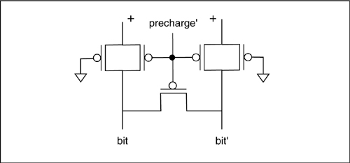
A precharging circuit for the bit lines is shown in Figure 6-30. Precharging is controlled by a single line. The major novelty of this circuit is the transistor between the bit and bit’ lines, which is used to equalize the charge on the two lines.
Figure 6-32: A dual-ported SRAM core cell.

Many designs require multi-ported RAMs. For example, a register file is often implemented as a multi-port SRAM. Each port consists of address input, data outputs, and select and read/write lines. When select is asserted on the ith port, the ith address is used to read or write the addressed cells using the ith set of data lines. Reads and writes on separate ports are independent, although the effect of simultaneous writes to a port are undefined. The circuit schematic for a two-port SRAM core cell is shown in Figure 6-32. Each port has its own pair of access transistors. The transistors in the cross-coupled inverters must be resized moderately to ensure that multiple port activations do not affect the stored value, but the circuit and layout designs do not differ radically from the single-ported cell.
Figure 6-31: Layout of a pair of SRAM core cells.

6.7.3 The Three-Transistor Dynamic RAM
The simplest dynamic RAM cell uses a three-transistor circuit [Reg70]. This circuit is fairly large and slow. It is sometimes used in ASICs because it is denser than SRAM and, unlike one-transistor DRAM, does not require special processing steps.
Figure 6-33: Design of a three-transistor DRAM core cell.
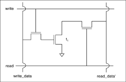
The three-transistor DRAM circuit is shown in Figure 6-33. The value is stored on the gate capacitance of t1; the other two transistors are used to control access to that value:
• To read, read_data’ is precharged to VDD. We then set read to 1 and write to 0. If t1’s gate has a stored charge, then t1 will pull down the read_data’ signal, else read_data’ will remain charged. Read_data’, therefore, carries the complement of the value stored on t1.
• To write, the value to be written is set on write_data, write is set to 1, and read to 0. Charge sharing between write_data and t1’s gate capacitance forces t1 to the desired value.
Substrate leakage will cause the value in this cell to decay. The value must be refreshed periodically—a refresh interval of 1 ms is consistent with the approximate leakage rate of typical processes. The value is refreshed by rewriting it into the cell, being careful of course to rewrite the original value.
6.7.4 The One-Transistor Dynamic RAM
The one-transistor DRAM circuit quickly supplanted the three-transistor circuit because it could be packed more densely, particularly when advanced processing techniques are used. The term one-transistor is somewhat of a misnomer—a more accurate description would be one-transistor/one-capacitor DRAM, since the charge is stored on a pure capacitor rather than on the gate capacitance of a transistor. The design of one-transistor DRAMs is an art beyond the scope of this book. But since embedded DRAM is becoming more popular, it is increasingly likely that designers will build chips with one-transistor DRAM subsystems, so it is useful to understand the basics of this memory circuit.
Figure 6-34: Circuit diagram for a one-transistor DRAM core cell.

Figure 6-34 shows the circuit diagram of a one-transistor DRAM core cell. The cell has two external connections: a bit line and a word line. The value is stored on a capacitor guarded by a single transistor. Setting the word line high connects the capacitor to the bit line. To write a new value, the bit line is set accordingly and the capacitor is forced to the proper value. When reading the value, the bit line is first precharged before the word line is activated. If the storage capacitor is discharged, then charge will flow from the bit line to the capacitor, lowering the voltage on the bit line. A sense amp can be used to detect the dip in voltage; since the bit line provides only a single-ended input to the bit line, a reference voltage may be used as the sense amp’s other input. One common way to generate the reference voltage is to introduce dummy cells which are precharged but not read or written. This read is destructive—the zero on the capacitor has been replaced by a one during reading. As a result, additional circuitry must be placed on the bit lines to pull the bit line and storage capacitor to zero when a low voltage is detected on the bit line. This cell’s value must also be refreshed periodically, but it can be refreshed by reading the cell.
Figure 6-35: Cross-section of a pair of stacked-capacitor DRAM cells.

Figure 6-36: Cross section of a one-transistor DRAM cell built with a trench capacitor.

Modern DRAMs are designed with three-dimensional structures to minimize the size of the storage cell. The two major techniques for DRAM fabrication are the stacked capacitor and the trench capacitor. The cross-section of a pair of stacked capacitor cells is shown in Figure 6-35 [Tak85]. The cell uses three layers of polysilicon and one level of metal: the word line is fabricated in poly 1, the bottom of the capacitor in poly 2, and the top plate of the capacitor in poly 3. The bit line is run in metal above the capacitor structures. The capacitor actually wraps around the access transistor, packing a larger parallel plate area in a smaller surface area. The bottom edge of the bottom plate makes the contact with the access transistor, saving additional area. The trench capacitor cell cross-section is shown in Figure 6-36 [Sun84]. A trench is etched into the chip, oxide is formed, and the trench is filled with polysilicon. This structure automatically connects the bottom plate to the grounded substrate; a contact is used to directly connect the polysilicon plate to the access transistor.
One should not expect one-transistor DRAMs that can be fabricated on a logic process to be equivalent to commodity DRAMs. The processing steps required to create a dense array of capacitors are not ideal for efficient logic transistors, so high-density DRAMs generally have lower-quality transistors. Since transistors make up a relatively small fraction of the circuitry in a commodity DRAM, those chips are optimized for the capacitors. However, in a process designed to implement large amounts of logic with some embedded DRAM, processing optimizations will generally be made in favor of logic, resulting in less-dense DRAM circuitry. In addition, the sorts of manufacturing optimizations possible in commodity parts are also not generally possible in logic-and-DRAM processes, since more distinct parts will be manufactured, making it more difficult to measure the process. As a result, embedded DRAM will generally be larger and slower than what one would expect from evaluating commodity DRAM in a same-generation process. However, substantial performance gains can be obtained simply by eliminating chip-to-chip connections, as shown in the next example.
Example 6-2: A processor-in-memory system
The EXECUBE processor [Kog95] is known as a processor-in-memory system since it integrates CPUs on a dynamic RAM chip. The prototype EXECUBE has eight processing elements (PEs). Each PE includes a 16-bit CPU and 32 kilobytes of dynamic RAM. Since each CPU has its own block of DRAM, all the processors can perform simultaneous independent memory accesses. Here is a photomicrograph of an EXECUBE chip, showing the eight PE and memory subsystems:
Photo © 1996 IEEE.

Integrating the CPU and memory has three main advantages. First, much higher memory bandwidth is allowed, since the width of a memory access is not limited by the available pins. Second, because pins are not limited, the wide memory can be divided into multiple addresses. Typical microprocessors read a single sequence of bytes to reduce the number of address bits required, while the EXECUBE can read seven uncorrelated addresses simultaneously. Third, power consumption is greatly reduced—a 50 MHz EXECUBE processor fabricated in 0.8 μm technology consumes only 2.7 Watts.
6.8 Field-Programmable Gate Arrays
A field-programmable gate array (FPGA) is a block of programmable logic that can implement multi-level logic functions. FPGAs are most commonly used as separate commodity chips that can be programmed to implement larger functions than can be fit into a programmable logic device (PLD). However, small blocks of FPGA logic can be useful components on-chip to allow the user of the chip to customize part of the chip’s logical function.
An FPGA block must implement both combinational logic functions and interconnect to be able to construct multi-level logic functions. There are several different technologies for programming FPGAs, but most logic processes are unlikely to implement anti-fuses or similar hard programming technologies, so we will concentrate on SRAM-programmed FPGAs. A programmable interconnect point can be constructed by using a pass transistor to connect two wires and controlling its gate by the value stored in an SRAM cell. When the SRAM cell stores a logic 1, the pass transistor will connect the two wires. A combinational logic block must be able to implement any combinational function of n bits, depending on its programming. This functionality is equivalent to a truth table. A block of SRAM can be used to implement the truth table—the address determines the row of the truth table required by the current value of the combinational inputs, while the value stored at that address is the function’s output. Combinational logic blocks typically include a flip-flop which can be selectively connected between the combinational output itself and the programmable wiring connected to the block; adding the flip-flop simplifies programming in many cases.
6.9 Programmable Logic Arrays
The programmable logic array (PLA) is a specialized circuit and layout design for two-level logic. While the PLA is not as commonly used in CMOS technology as in nMOS, due to the different gate circuits used in the two technologies, CMOS PLAs can efficiently implement certain types of logic functions.
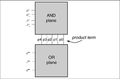
The architecture of a PLA, as shown in Figure 6-37, is very simple: it uses two levels of logic, one implementing the ANDs (called product terms) and another implementing the ORs. One of the best features of the PLA is that it can compute several functions at once, which can share product terms. Two-level functions are built from both the true and complement forms of the variables, so the inputs supply both forms, usually with a pair of inverters on the true form as buffers. Some sort of buffer is usually placed at the output. The architecture also suggests the attractiveness of the layout: the inputs to the AND plane flow vertically, while the outputs flow horizontally and emerge at the right side. The OR plane is simply a 90° rotation of the AND plane.
Such a layout can be very compact, but we need to find a gate structure compatible with this layout organization.
Figure 6-37: Organization of a PLA.
We clearly cannot use fully complementary gates for this layout style—wiring both the pullups and pulldowns would be too complex. The most common form of the CMOS PLA uses precharged gates for both AND and OR planes [Sho88]. Using a non-complementary gate lets us use very regular layouts for the wires: input signals are evenly spaced in one direction and output signals are also evenly spaced in the perpendicular direction. Figure 6-38 shows a logic diagram for a doubly-precharged PLA drawn to correspond with the layout. The product term lines p1, etc. flow from the AND plane to the OR plane. The circuits in the AND and OR planes are identical, except for programming transistors, which determine the PLA’s personality. In the AND plane, each precharged gate’s output node runs vertically through the cell. Pulldowns run between the output node and VSS lines which run parallel to the output lines; inputs run horizontally to be attached to the pulldowns’ gates.
The AND/OR plane is very simple to generate. We first lay down a grid of wires for input signals, VSS, and output signals. We can create a pulldown transistor at the intersection of input and output signals by adding small amounts of diffusion and poly along with a via. The pulldown can be added to the wiring by superimposing one cell on another; the pulldown cell is called a programming tab thanks to the shape of the transistor and via. The same cell can be used for both planes since the OR plane is simply a 90° rotation of the AND plane. Figure 6-39 shows a section of an AND/OR plane with four inputs running vertically in poly and two outputs running horizontally in metal1. Each pair of input lines shares a ground line running in n-diffusion; pairs also share open space for a programming tab’s via, so that one via can be used for two pulldown transistors on opposite sides of the via.
Figure 6-38: Internal architecture of a PLA. (Masakazu Shoji, CMOS Digital Circuit Technology © 1988, p. 220. Adapted by permission of Prentice Hall, Englewood Cliffs, New Jersey.)

Figure 6-39: A section of a PLA AND/OR plane.

The delay through the PLA is determined largely by the load introduced by the vertical and horizontal wires. The neat layout of the PLA keeps us from using large transistors in the pulldowns to speed up the gates—a large pulldown would not only add blank space down the entire row but would also lengthen the perpendicular wires. This doubly-precharged structure also complicates clocking.
Which functions are best implemented as PLAs? Those functions which are true for about half their input vectors are well-suited. If the PLA has very few programming tabs, we are wasting most of its area and are probably better off using fully complementary gates. If the PLA is nearly full, we can complement the functions to produce a nearly empty PLA. PLAs are also good for implementing several functions that share many common product terms, since the AND-OR structure makes it easy to send one product term to many different ORs. CPU microcode often has these characteristics.
Standard two-level minimization algorithms can be used to optimize the PLA personality. An optimization unique to PLAs is folding. If one region of the PLA is empty of programming tabs, it may be possible to remove that section and fold another section of the PLA into the newly freed space. Folding can leave the PLA with inputs and outputs on all four sides. While folding can dramatically reduce the size of the PLA, it also makes the PLA’s layout very sensitive to changes. A small change in the logic may require a use of a single programming tab in the region removed for folding, enough to undo the entire folding operation. Folded PLAs may, with a small logic change, unfold themselves like origami pieces in the middle of a chip design, destroying floorplans which relied on the small size of the folded PLA. As a result, PLA folding is less popular today than it was when PLAs first came into common use.
6.10 References
Introduction to Algorithms by Cormen, Leiserson, and Rivest [Cor90] includes a detailed comparison of the computational complexities of various addition and multiplication schemes. As they point out, asymptotically efficient algorithms aren’t always the best choice for small n. I am indebted to Jack Fishburn for an explanation of transistor sizing in carry chains. Books by Shoji [Sho88] and Glasser and Dobberpuhl [Gla85] describe circuit designs for interesting components; The MIPS-X RISC Microprocessor [Cho89] provides a good survey of the components used for a CMOS microprocessor. Hodges and Jackson [Hod83] give a good introduction to RAM and ROM design; more detailed discussions can be found in Glasser and Dobberpuhl and Shoji. The static RAM layout of Figure 6-31 was designed by Kirk Nolan of Princeton University. Keitel-Schulz and Wehn [Kei01] discuss embedded DRAM technologies.
6.11 Problems
6-1. Produce a complete table of the barrel shifter’s possible operations. List all possible combinations of top and bottom inputs and the resulting operation.
6-2. Identify the critical delay path through the barrel shifter.
6-3. Design a logic gate network for the full adder:
a) using two-level logic;
b) using multi-level logic.
6-4. What combination of input values produces the longest delay through a Manchester carry chain?
6-5. The output of an adder feeds one input to a second adder; the second adder’s other input comes directly from a primary input. Sketch the critical delay path through this system of two adders.
6-6. What is the false delay path in the carry-skip adder?
6-7. Design a stick diagram for a serial adder cell.
6-8. Design a one-row layout of a four-bit carry lookahead unit. You can use inverters and two- and three-input NANDs and NORs in the design.
a) Show the desired locations of primary inputs and outputs around the edge of the cell.
b) Show your decomposition of the functions into gates.
c) Show a good placement of the gates in the row and explain your criteria for judging the layout.
d) Sketch the design of the wiring channel underneath the gates, showing where wires enter and exit and their assignment to tracks in the channel.
6-9. Consider an ALU design:
a) Enumerate all the possible functions of a two-input ALU.
b) For each possible function, list the control inputs to the three function blocks of the three function block ALU.
6-10. Design the logic for an ALU that can perform these functions: addition, subtraction, AND, OR, NOT.
6-11. Develop stick diagrams for an unsigned array multiplier:
a) Draw stick diagrams for the full adder used in the core cell and for a carry-skip adder to be used in the final stage.
b) Draw a hierarchical stick diagram for the full array showing the layer assignments and organization of wires and cells.
6-12. Draw a block diagram for an array multiplier that uses Booth encoding. Use the adder-subtractor as a basic building block of the array.
6-13. Design components of a Booth multiplier:
a) Design the logic for one bit of the adder-subtracter.
b) Design a stick diagram for your adder-subtractor.
6-14. Design and analyze an 8 × 8 Wallace tree multiplier:
a) Draw the block diagram for an eight-bit carry save adder.
b) Draw the complete block diagram for the multiplier.
c) Draw a basic floorplan for the multiplier including the partial product generators and Wallace tree.
d) Identify the critical delay path through the multiplier.
6-15. Show how a bit-serial adder adds the two numbers a = 0101 and b = 0110 (these numbers are written here with the MSB first). Show the adder’s inputs and outputs for every clock cycle until the addition is complete.
6-16. How many groups must node capacitances be split into to properly simulate an SRAM at the switch level?
6-17. What is the minimum-delay encoding for a modulo-8 counter?
6-18. What is the relationship between a truth table and the pattern of programming tabs in a PLA’s AND and OR planes?