
Porous silicon gas sensors
Abstract:
This chapter discusses the use of porous silicon (PSi) for gas sensors. It is of great importance to develop efficient and economically viable gas sensors for different applications. PSi can be used as an alternative material for gas sensors, operating at a relatively low temperature, including room temperature. The interest in this material is mainly due to its extremely high surface-to-volume ratio, the ease of its formation and its compatibility with modern silicon microelectronics fabrication technologies. A large variety of different sensors made of PSi have been manufactured in recent years, and achievements in this field are reported in this chapter.
12.1 Introduction
There is a growing interest in developing efficient and economically viable gas sensors for detecting the leakage of different gases into the atmosphere. Environment air quality has improved considerably in the last few decades due to modern air pollution legislation. However, there is strong evidence suggesting that exposure to air pollution, even at the levels commonly achieved nowadays in developed countries, leads to adverse health effects. In particular, the content of ozone, hydrogen and nitrogen dioxide has been found to be too high in many cities in the USA, Europe and Asia. Many semiconductor gas sensors have been developed in 30 years, mainly based on metal oxide semiconductors such as SnO2, ZnO, TiO2, etc (see, for example, the review paper by Aroutiounian (2007)). A high operating temperature (sometimes up to several hundred degrees Celsius) and high electric power consumption are limitations of the majority of such hydrogen gas sensors (Boon-Bret et al., 2009, 2010). Although hydrogen sensors working at nearly room temperature have been developed recently (Adamyan et al., 2007; Aroutiounian, 2012), the temperature and power limitations remain for other important gases.
PSi can be used as an alternative material for gas sensors, as it requires a relatively low level of preheating in order to operate (up to room temperature). The interest in this material is mainly due to its extremely high surface-to-volume ratio, the ease of its formation and its compatibility with modern silicon microelectronics fabrication technologies. Usually, PSi is electrochemically formed by anodic dissolution of silicon in a hydrofluoric solution. Passing an electric current between the acid electrolyte and the Si sample leads to the formation of an array of deep narrow pores. Pores with diameters from nanometers up to micrometers deep have been achieved. PSi exhibited strong visible luminescence at room temperature (Canham, 1990; 1997). Canham’s discovery opened up the possibility of developing silicon-based optoelectronic devices, fabricating Si quantum wires and pillars of crystalline Si only a few nanometers wide etc. (Pavesi et al., 2004). Depending on the electrolysis conditions and the illumination level, a porous texture with pore diameters varying from 2 nm to 15 nm and with a density varying from 20% to 80% of that of the original substrate can be realized (Foucaran, 1997). Many theoretical works were carried out in order to understand the processes of such a porous texture (for example, a simple model based on dangling bonds was proposed to explain quantitatively observed phenomena (Stievenard and Deresmes, 1995)).
PSi attracted the attention of specialists in photovoltaics for the manufacture of antireflection coatings (ARC) for silicon solar cells (Yerokhov, 1999; Adamyan et al., 2000; Aouida et al., 2004). Calculations of the reflectance of such PSi coatings have been carried out (Aroutiounian et al., 2004; 2006a; 2006b; 2007; 2008; Martirosyan et al., 2007) using the optical matrix approach method. Dramatically lower reflectance within a larger energy range that includes the ultraviolet, visible and infrared regions of the solar spectrum can be realized in the case of diamond-like carbon (DLC)/PSi and silicon oxynitride/PSi double layers, as proposed by the authors, during comparison with the spectra obtained that are usually used in SiO2/TiO2 ARC solar cells. Investigations of the influence of different gases on the properties of coatings will be carried out.
A large variety of different sensors made of PSi has been fabricated over recent years. The detection and quantification of bacterium, viruses and other organic materials, including DNA, measured by PSi sensors have been reported (Saha, 2008; Miller, 2012). The properties of gas sensors will be discussed below.
12.2 Conductivity and capacitance sensors
The capacitance and the conductance of a porous layer depend on its porosity (i.e. the size and distribution of pores, which can vary from mesopores to micro- and nano-pores). Capacitance and conductance are also affected by controlling the etching current density, etching time, the concentration of the electrolyte, and the intensity and wavelength of the illumination (Baratto et al., 2002). Gas molecules in a PSi-based gas sensor are adsorbed on the surface of the PSi layer and diffuse into the porous bulk. Condensation of the diffused gas may occur inside pores that have radii less than a critical value called the ‘Kelvin radius’ (Saha, 2008).
The differences in permittivity are directly related to the gas concentration level in the environment. A theoretical model was proposed by Saha (2008) in order to explain the change in the dielectric constant of the PSi layer and to provide a theoretical basis for optimizing the porosity and pore morphology of the PSi layer. This model considers PSi as a three-phase mixture of dispersed spherical particles consisting of silicon nano-particles, silicon oxides and voids. The sensitivity of the PSi layer to a particular gas is due to the adsorption of the gas molecules on its surface, as well as the condensation inside the pores. A change in the dielectric constant of the matrix can affect the channel conductivity in a metal oxide semiconductor field effect transistor (MOSFET) and in p–n junction gas sensors. An interaction with dangling bond states may also lead to adsorbate-induced conductance changes. Peculiarities of the conductivity in PSi have been studied theoretically, for example by Aroutiounian and Ghulinyan (2003). An analytical study of the dependence of PSi conductivity on porosity has been made. It was found that, for porosities much lower than the percolation threshold of 57%, conductivity is mainly crystalline, while fractal behavior is observed at porosities near the percolation threshold. Quazi-one-dimensional hopping is expected at higher values of porosity.
In certain papers (Aroutiounian and Ghulinyan, 2000; Aroutiounian et al., 2000), a fractal model of a porous layer formation was proposed. The consideration of the time-dependent pore growth process has allowed us to calculate important parameters of the porous matrix, such as the formed surface area, and the surface and volume porosity values. We have theoretically shown that the formed surface area is strongly dependent on the difference between the pore size growth velocities parallel and perpendicular to the surface (i.e. the crystallographic orientation of the silicon surface). The volume and surface porosity values and the formed porous surface area are linear functions of the density of the anodization current. These results are in agreement with other theoretical and experimental data.
The condensation of vapors inside nanometric PSi structures has been investigated (Moretti et al., 2007). The liquid phase covers the pore surface as a thin film and fills a volume fraction in the sponge-like structure depending on the physical and chemical properties of each compound. The filling factor of different substances can be measured as a function of fractal-like PSi film porosity by means of an interferometric technique. The capillary condensation exhibits a nonlinear behavior at high porosities (greater than 0.8).
A simple nondestructive capacitance method is proposed (Adamyan et al., 2006) for the determination of basic PSi parameters such as layer thickness, porosity and dielectric permittivity. The method is based on two comparative measurements of the capacitance of the metal/PSi/single crystalline silicon/metal structure: one measurement is taken when there are air-filled pores, while the other measurement involves pores filled by an organic compound with a high value of dielectric permittivity. Comparison of results obtained in Adamyan et al. (2006) by the ball lap and the gravimetric techniques before and after anodization, with the data of capacitance measurements carried out with the same samples prior to their destruction, shows sufficiently good agreement.
12.3 Luminescence from PSi
In 1990, Canham observed intense visible photoluminescence (PL) from PSi at room temperature. Visible luminescence ranging from green to red in color was soon reported for other PSi samples and ascribed to quantum size effects in wires of width ~ 3 nm (Ossicini et al., 2003). Several models of the origin of PL have been developed, from which we chose two. In the first (the defect model), the luminescence originates from carriers localized at extrinsic centers that are defects in the silicon or silicon oxide that covers the surface (Prokes, 1993). In the second model (Koch et al., 1996), absorption occurs in quantum-confined structures, but radiative recombination involves localized surface states. Either the electron, the hole, both or neither can be localized. Hence, a hierarchy of transitions is possible that explains the various emission bands of PSi. The energy difference between absorption and emission peaks is explained well in this model, because photoexcited carriers relax into surface states. The dependence of the luminescence on external factors or on the variation of the PSi chemistry is naturally accounted for by surface state changes.
The most widely-studied PL occurs in the far-red to orange-yellow wavelengths. Red PL is the only wavelength that can be electrically excited. This PL shows a blue shift with an increase in anodization current density. We noted that the porosity of PSi increases with an increase in anodization current density, which leads to a decrease in the dimensions of Si nanocrystals within the PSi. The blue shift of the PL and optical absorption with increasing porosity are the first important signs that quantum confinement plays a significant role in PSi. The splitting of the luminescent states, the polarization of the PL and the phonon replicas seen in the PL under resonant excitation can be observed. The PL peak wavelength and intensity are sensitive to the PSi surface, which makes the PL phenomena very responsive to different gases.
Balaguer and Matveeva (2010) have considered the phenomenon of PSi photoluminescence by molecular oxygen. Figure 12.1 shows the PL spectra of a freshly prepared PSi layer in N2 and O2 gases. The decrease of PL in oxygen is due to an interaction between excited PSi and the molecule that received a part of an emitted optical energy, transforming it into excited specie. This phenomenon is reversible and, after placing the layer in a N2 atmosphere, the PL is completely recovered (see second PL curve in N2 atmosphere in Fig. 12.1). Thus, energy transfer inside the system takes place without any chemical transformation of PSi. In other words, physicosorbed chemicals can quench PL without effecting any net chemical reaction at the surface (Lauerhass and Sailor, 1993), and such interactions are mainly reversible. There are many mechanisms that explain the quenching phenomenon. Changes in both spectral distribution and spectral intensity offer promising methods for the detection of gases. PSi-based sensors that use PL quenching technology allow the detection, for example, of gaseous NOx, Cl2, Br2, I2, O2, ethanol, methanol, benzene, toluene, xylene, freons, ethers and chlorinated carbons (Canham, 1997, p. 364). PSi sensors were fabricated and tested, using the PL quenching technique, in the presence of various linear aliphatic alcohols (methanol to n-hexanol) and water in the range of 10–100 ppm. The phenomenon of the PL quenching effect in the presence of target analytes is used in optical sensing. An increase in the degree of quenching was observed with the chain length of alcohols, while minimum response was given to water. Responses as high as 80–90% and an almost instant response time have proven the sensors to be highly efficient. Sensitivity, response and recovery time increased with the chain length of alcohols. Exceptional improvements in sensor response and recovery time were observed for methanol. From methanol to butane, the sensitivity was dependent on the effective concentration of analytes in the PSi matrix. For pentane and hexane, which have high boiling points, sensitivity was linked to the dielectric quenching mechanism, due to the condensation of vapors inside the pores.
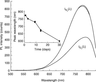
12.1 PL emission from the electrochemically prepared PSi layer on wafer in gas phase and different atmospheres: nitrogen ![]() and oxygen
and oxygen ![]() . Inset: evolution of the PL maximum peak position with ageing time. After Ballaguer and Matveeva (2010) with the permission of the authors.
. Inset: evolution of the PL maximum peak position with ageing time. After Ballaguer and Matveeva (2010) with the permission of the authors.
There are irreversible quenchers. Their molecules react with the inner surface of PSi by introducing efficient non-radiative charge carrier traps. Some chemical reactions lead to the generation of surface species that produce electronically passive interfaces. Other species are very efficient electron–hole recombination traps. For example, the reaction of PSi with chlorine, bromine or iodine gas leads to the introduction of Si–Cl, Si–Br or Si–J surface traps and complete quenching of PL (Canham, 1997, p. 364). PL is recovered upon air hydrolysis. Irreversible quenching was demonstrated in the case of the halogens, NOx and amines. Reversible quenching of PL had been detected following the reaction of the vapors of benzene, hexane, or dichloromethane, as well as gaseous molecules such as SO2 with PSi.
The PL quenching measurements of sensor elements based on prepared PSi, oxidized PSi and methyl-10-undecenoate functionalized PSi are reported by Dian et al. (2010). It was demonstrated that relatively simple functionalization of the PSi surface via oxidation and hydrosilylation with methyl-10-undecenoate substantially modifies the PL quenching response in the presence of polar analytes, as compared with H-terminated PSi surface.
PSi and porous polymer substrates for optical chemical sensors are discussed by Hajj-Hassan et al. (2010). They were used as substrates to encapsulate gaseous oxygen (O2) responsive luminophores in their nanostructured pores. These substrate materials behave as optical interference filters that allow efficient and selective detection of the wavelengths of interest in optical sensors.
A PSi microcavity was exposed to the saturated vapor of ethanol. The ethanol substitutes the air inside the pores and leads to a rise in a progressive monotonic red shift of the interference pattern of the PL spectrum. Moreover, the PL intensity of the cavity peak oscillates over time. Both effects are sequences in the progressive change of the refractive index of air and ethanol. Large, repeatable and selective red-shifts in the reflectivity spectra of PSi microcavities have been registered following exposure to vapors of aliphatic hydrocarbons with different molecular weights. The shift in the resonant peak of the optical microcavity is due to average refractive index changes. Vapors of HCl, NH3 and NO at the 10 ppm level, as well as isopropyl alcohol and aliphatic molecules, were detected by a PSi gas PL sensor (Vrkoslav et al., 2007; Acquaroli et al., 2010; Dian et al., 2010; Ong et al., 2010; Huang et al., 2011). The reflectivity spectrum and Fourier-transform data analysis was applied (Hutter and Ruschin, 2010) in order to enable simple discrimination between different ammonia and water vapor concentrations.
A distributed PSi Bragg reflector was used for optical interferometric sensing of organic vapor (Kim et al., 2011). A fully-integrable optical PSi-based Bragg grating waveguide sensor for chemical monitoring has been reported; the PSi had nanometric pores. PSi filters and preconcentrators have recently been realized since 2008, which opens new possibilities in the detection of chemical vapor (Salem et al., 2008; Camara et al., 2010; Jalkanen et al., 2011).
A theory for semiconductor nanostructure reactivity to a gas environment has been developed (Ninno et al., 2000) to link the nanostructure geometry of PSi to its optical properties. Light emission and absorption energies have been calculated within a variational scheme, which includes a position-dependent boundary condition. The results of measurements of both PL quenching and peak position shift in the presence of oxygen can be accounted for by the theory. The model can be considered as one of the first attempts to create a general theory governing the functioning of semiconductor nanostructure-based gas sensors.
12.4 Optical and photo properties of PSi sensors
The absorption and transmission spectra of PSi (Fig. 12.2) were considered (von Behren et al., 1998; Pavesi, 2004). Measurements of transmission spectra of several 20 μm thick, freestanding PSi films (made on 5–7 Ωcm p-type Si substrates of various porosities) and a 20 μm thick c-Si film have shown that the increase in porosity leads to an increase in transmission. Its shift in photon energy ranges from 2 eV up to 3.5 eV. The absorption spectra of bulk single-crystalline silicon and PSi with grains of different sizes (from 240 nm up to 410 nm) were measured. The absorption coefficient was 102 cm− 1 at photon energy 1.3 eV for single-crystalline grains and 2 eV for PSi grains of 240 nm. As expected, a further decrease in the size of PSi grains led to the transmission of photons having greater energies.
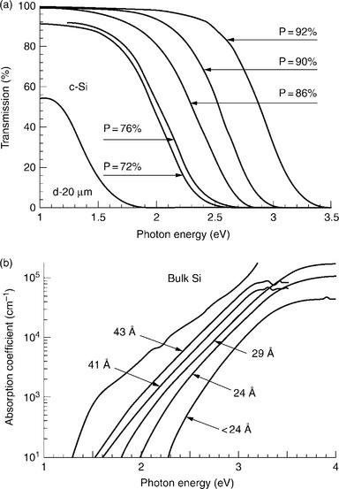
12.2 (a) Transmission spectra of several 20 μm thick freestanding PSi films (5–7 Ωcm p-type Si substrate) of various porosities (P) and a 20 μm thick c-Si (crystalline silicon) film. (b) Absorption spectra for Si nanocrystals with sizes from 4.3 nm to 2.4 nm deduced from the transmission spectra of (a). The absorption of c-Si is shown for comparison. The saturation beyond 3 eV is an artifact of the measurement procedure. After von Behren et al. (1998) with the permission of the authors.
The features of optical absorption and emission in PSi have been discussed by Alexanyan et al. (2003). An allowance for the finite nature of the potential well depth when calculating the shift of the absorption edge of the quantum wire, as well as the probability of transition between states in conduction and valence bands, along with the radiation lifetime, is shown to introduce significant amendments into the dependences of these parameters on the size of quantum wire in PSi.
It has been shown that the refractive index of a material is proportional to its porosity (Pavesi, 2004). Therefore, complex structures can be realized using PSi etched layers. Moreover, the refractive index of PSi can be changed by the current density during the etching. A current profile is reflected in a correlated in-depth refractive index profile. This allows the formation of microcavities, Bragg reflectors, an optical delay line etc. If a crystal has uniaxial symmetry, a crystal possessing such as anisotropic dielectric properties is said to be ‘birefringent’. The optical anisotropy in PSi is due to the anisotropic geometry of the pores and depends on the crystalline orientation of the silicon substrate. Birefringence has been reported in (100), (111) and (110) oriented PSi. The optical form of the birefringence property of PSi is used in a compact polarization interferometer to demonstrate a novel optical transduction mechanism for vapor- or gas-sensing applications. This technique uses high interferometric sensitivity of the polarization interference intensity when the PSi sample is exposed to solvent vapors. Heptane and ethanol vapors were detected (Liu et al., 2002).
Anisotropically nanostructured silicon layers exhibit a strong inplane birefringence. Their optical anisotropy parameters are found to be extremely sensitive to the presence of dielectric substances inside the pores. Polarization-resolved transmittance measurements provide an extremely sensitive tool with which to analyze the adsorption of various gases in negligible quantities; this makes these layers a good candidate for sensor applications. A highly-sensitive recognition element based on birefringent PSi layers has been realized.
In multiparametric PSi optical microcavities, developed by Baratto et al. (2002), three independent quantities can be measured: the electrical conductance, the PL intensity and the wavelength of the optical resonance. The change of these parameters as a function of NO2 (0.5–5 ppm), ethanol (300–15000 ppm) and relative humidity (0–100%) has been investigated.
A gas sensor for simultaneous monitoring of the electrical and optical properties developed by Jalkanen et al. (2010) is based on a PSi optical interference filter layer. This was produced with an electrochemical etching process. Sensors with differing hygroscopic properties were produced, and their response to atmospheric variations was tested. This sensor had a rapid response and an increased level of selectivity between different gases. In tests, the sensor response changed according to humidity. The sensors were sensitive to ethanol and dimethylformamide vapors. The size of such sensing elements was reduced.
A new method for using photo-electromotive force (Photo-EMF) in the detection of gas and for controlling sensitivity is proposed (Vashpanov et al., 2011). Photo-EMF on the heterojunction between the PSi thin layer and the crystalline silicon wafer depends on the concentration of ammonia in the measurement chamber. A light-transparent contact to the porous Si was formed. Photo-EMF sensitivity corresponding to the ammonia concentration in the range from 10 ppm to 1000 ppm can be controlled by the intensity of the source of illumination.
12.5 PSi noise sensors
The sensitivity of gas sensors is mainly measured by the classical method of a comparison of the ohmic resistance of the sensors in gas media and air. However, excellent results have been obtained by studying and comparing the low-frequency noise characteristics of sensors to determine their sensitivity.
In Paremuzyan and Aroutiounian (2012a, 2012b), the phenomenon of a reduction in the heat of adsorption was taken into account using the results of Langmuir’s theory. The noise for oxygen and other type of gases was calculated.
We studied experimental samples of PSi-layered structures Au/PSi/SCS/Al (SCS being single crystal silicon) (Mkhitaryan et al., 2007a, 2007b; Aroutiounian et al., 2008). The PSi layer was formed by electrochemical etching on a substrate made of heavily doped p + –type silicon with orientation (100) and resistivity of 0.01 Ωcm. The samples were ~ 2 μm thick. The reverse of the wafer was coated with an Al film 20–30 nm thick. The top contact was of gold sprayed on the surface of PSi and had a diameter of 1.5 mm. Conductive glue based on silver ‘conductive epoxy’ was used for the top contact. The porosity of PSi films was 50% and 73%.
Measurements of current–voltage characteristics (CVCs) of the above-mentioned structures were carried out at room temperature in air and in mixtures of air with different concentrations of carbon monoxide. The typical CVCs of samples with a porosity of 73% in all environments have a nonlinear behavior. The CVC is nonlinear for low back bias, but becomes linear with an increase in low back bias. The CVCs for PSi of 73% porosity, both in air and in air + 0.4% СО, have rectifying characteristics, but, as compared with the corresponding characteristics of samples with 50%-PSi, a sharp decrease in conductivity and an absence of current saturation took place. The factor of ideality m was estimated from the initial part of the direct branch. The barrier height was determined from the linear part of the backward branch of the CVC.
A model where the resistance RS of the heterojunction interface PSi/Si-single crystal is connected in series with the base resistance of the PSi layer was applied for the study of CVCs. As in the field of small direct bias, the voltage drop is insufficient and displacement on the base resistance may be ignored; the initial part of the direct branch is approximated by the exponential dependence of current J on voltage U with a large factor of ideality m:
Here q is electron charge, k is the Boltzmann constant and T is temperature. The factor m can be estimated from Equation [12.1].
We observed that a change in the structure of the experimental environment resulted in the change of CVCs both in the direct displacement region and in the region of backward displacement. Essentially, the current grows in both regions at the same displacement with the introduction of CO into the air.
A reduction of the height of a heterojunction barrier took place because of the migration of CO molecules into pores of the heterojunction interface. This is one of the reasons for the high gas response of the heterostructure containing a nanosize porous film. However, the mechanism of the high gas-sensitivity of porous structures is not yet completely understood. Analysis of experimental data has shown that the gas adsorption of CO molecules leads to a decrease in the height of the heterojunction barrier. It is accompanied by the reduction of the PSi layer base resistance, which is connected in series with the heterojunction. The degree of decrease in the barrier height VB depends on the amount of CO in the air. Numerical estimations of the Rs, m and VB values were carried out. Depending on content, the value of m for PS-73%, is changed from 21 to 9.5 for air and air + CO.
A sharp drop, by several orders of magnitude, of SU (f)/U2 with the change in concentration of CO in the air suggests the possibility of making a precise estimation of the gas content in air – that is, we can offer a new method of estimation of the concentration of gases in an environment and the noise spectroscopy (Figs 12.3 and 12.4). SU is the spectral density of the noise voltage.
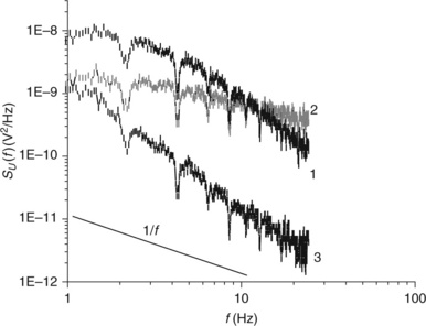
12.3 Noise spectra for samples with the 50%-porosity PSi layers exposed to the indicated gases at a current of 0.1 mA. The straight line refers to ‘classical’ 1/f noise. Samples were placed in air (1), air + ethyl alcohol vapor (2) and air + 1.7% CO (3).
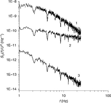
12.4 Normalized noise spectra for samples with the 50%-porosity PSi layers exposed to the indicated gases at a current of 0.1 mA. Samples were placed in air (1), air + 0.4% CO (2) and air + 1.7% CO (3).
It is known that the parameter αH is determined for the frequency 10 Hz from the empirical Hooge’s formula:
Here, N is the number of free carriers in a sample, αH is the dimensionless Hooge parameter, U is the voltage applied to the studied structure, γ is the frequency index (which is usually approximately equal to unity) and δ ≈ 2 The values of SU, Uδ and γ were determined experimentally from the spectra obtained. Parameter γ (in air) was equal to 0.5; γ (in air + 0.4% CO) = 1, γ (in air + 2% CO) = 1.3. Comparison of αH values shows that, for crystal materials, αH are several orders of magnitude higher than for noncrystalline structures: αH can take values from 1 up to 104. One of the reasons for this is the low mobility of charge carriers in disordered materials, to which category PSi also belongs. The nonuniformity of the current density in the sample may also cause a large value of αH. In our case, this can probably be caused by the nano-crystalline structure of the PSi layer. The nonuniform density of the current in the nano-crystallite arises for several reasons: (а) the corallike systems of variable cross-section silicon strings, (b) the presence of the depletion region around each pore, and (c) inhomogeneity of the density and mobility of free charge carriers. It was observed that the value of αH varies after the introduction of carbon oxide (CO) into the air; namely αH increases with the increase in the concentration of CO in air. We explain this as follows: with an increase in the concentration of gas molecules, the number of molecules (ions) adsorbed on a surface increases and therefore the density of traps located at the PSi/SCS interface increases. The heterobarrier height at gas adsorption decreases with an increase in the adsorbate concentration. Therefore, the effect of a potential barrier, in comparison with increasing concentration of surface traps, becomes less important.
So, the SU (f) value grows with the increase in porosity of silicon and in the concentration of polar CO molecules in air. Correspondingly, the noise parameter αH varies also. Noise spectra of the structures investigated in various gas media in the low-frequency range were quantitatively different and displayed different characteristics. The physics of the noise phenomena in a system containing a gas-semiconductor structure is rather complicated. The possible reasons for large values of γ and αH for PSi samples in air and their increase in the gas chamber are discussed below.
As seen from our measurements, the values of the spectral density of the noise voltage change to a significant degree when samples are placed in different gas media and air. Therefore, we have compared the gas response of sensors made using different technologies. We compared data for Figaro TGS 2443, 2511, 3870 and 821 sensors, as well as our sol–gel H2 and PSi sensors (Paremuzyan and Aroutiounian, 2012b). The response of this range of sensors was earlier measured by the classical method of comparison of the resistance of sensors in gas media and air. Here, we reported results of the study of low-frequency noise characteristics of the metal–PSi–silicon single crystal–metal structure with differing porosities of PSi. The study was performed in dry air and in a mix of dry air with CO, hydrogen and alcohol at different concentrations. A calculation of the response of the porous structures under investigation was carried out using results obtained during an experiment for changes in target gas media and air of resistance Gdc = Rsa / Rtg (in the ohmic element of CVCs) а nd of the spectral density of noise (SND) due to voltage fluctuations:
We introduced the results of measurements of the response of the Figaro sensors and our samples made of SnO2 and PSi (Figs 12.5 and 12.6) (Aroutiounian et al., 2009). We see from Figs 12.5 and 12.6, the dc resistance response Gdc, measured by the classical method, led to smaller values of the sensitivity (response) in comparison with the SND sensitivity. It allows the carrying out of fuctuation-enhanced measuring of sensor response.
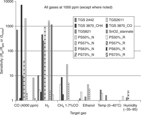
12.5 Sensitivity of different sensors to gases. We compare data for Figaro sensors TGS 2442, 2611, 3870 and 821, as well as our sol–gel H2 and PSi sensors.
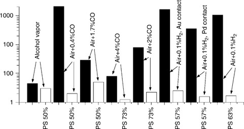
12.6 Comparison of the sensitivity of different sensors obtained by measurements using classical resistivity (GR) and noise (Gnoise) methods. GR, open bars; Gnoise, black bars. The values of sensitivity (response) are compared for measurements by the noise (black) and resistance (white) methods.
A discussion of changes of parameter αH in Hooge’s formula in gas media suggests that αH increased with the increase in concentration of CO in air. The explanation for this is that, with the increase in the concentration of CO, the number of molecules (ions) adsorbed on a surface increases; therefore, the density of traps located at the PSi/SCS interface increases. The heterojunction barrier height at gas adsorption decreases with the increase in the adsorbate concentration. Therefore, the effect of a potential barrier, in comparison with increasing concentration of surface traps, becomes less important. Nonuniform density of the current in the nano-crystallite arises for several reasons: (а) the coral-like systems of variable cross-section silicon strings, (b) the presence of the depletion region around each pore, and (c) inhomogeneity of the density and mobility of free charge carriers.
12.6 Different PSi gas sensors
Barillaro et al. (2010, 2009) have presented PSi junction field effect (JFET) transistor gas sensors. They are an integrated p-channel JFET device modified with a PSi layer which acts as a sensing element to both synthetic air and NO2 with concentrations of 100, 300 and 500 ppb at room temperature. The quantitative information on the effect of the NO2 adsorption/desorption at the PSi surface on conductance and surface charge density of PSi was obtained.
In Barillaro et al. (2008), nitrogen dioxide detection by using p + –n silicon diodes surrounded by a PSi layer was demonstrated. Adsorption of NO2 in the PSi layer modifies the electrical properties of the PSi/crystalline silicon interface and, in turn, the p + –n diode current. The device shows a higher selectivity to NO2 in comparison with ethanol, at any polarization voltage and relative humidity level.
A novel PSi sensor for the detection of 0.1–10 ppm of NO2 was sensitive simultaneously to 200 ppb of O3, 1000 ppm of CO, 20 ppm of benzene, organic vapors and humidity. At low concentration (100 ppb) of NO2, the interference from ozone benzene, CO and organic vapors was not detected (Baratto et al., 2001).
Pancheri et al. (2003) have reported sensitivity to 12–50 ppb NO2 at room temperature in the sensor, based on the change in conductivity of a single meso-porous Si layer with about 80% porosity. Meso-porous Si shows higher sensitivity and better selectivity for NO2, while macro-porous Si shows better selectivity for NH3 (Sun et al., 2012). The light-enhanced NO2 sensing properties of PSi at room temperature have been demonstrated (Chen et al., 2012).
The Pd-sensitized PSi H2 sensor with a thin zinc oxide (ZnO) over-layer demonstrated improved gas response behavior at higher temperatures (Kanungo et al., 2010a). PSi was produced during a gas sensor study with the Pd–Ag/Pd:ZnO/Pd:PSi/Si/Al structure indicating that the Pd-sensitized ZnO on Pd-modified PSi exhibits consistent H2-sensing performance, including improvements in gas response, the response time and long-term stability. However, recovery took considerable time.
Effects of surface passivation in PSi as a H2 gas sensor were also investigated (Ali et al., 2008). A peroxide-based PSi sample fabricated as a H2 gas sensor showed better electrical (I–V) sensitivity compared with those without peroxide, which has been associated with good surface passivation. Surface passivation in peroxide-based PSi is also maintained at higher temperatures (100 °C).
PSi samples coated with a continuous palladium layer in an electro less process were reported in Razi et al. (2010). I–V curves of Schottky-like Pd/PSi samples were measured in air and in hydrogen. The samples can sense H2 in a wide range of concentrations (100–40000 ppm) without any saturation behavior. Hydrogen-sensing properties of these samples were investigated at room temperature for a duration of nine months. Sample sensitivity (response time) decreased to a saturated value after 45 days. The effect of different porosities on the performance of the Pd-Ag modified PSi H2 sensor in a metal-insulator-semiconductor (MIS) configuration was studied at room temperature and for long-term performance (Kanungo et al., 2009c, 2010b). Improved sensing was reported for 55% porosity. Ni-PSi-Ni H2-sensitive diodes with Schottky contacts (Naderi et al., 2012).
Pd and WO3/Pd MIS gas-sensitive structures based on PSi layers have been studied by Solntsev et al. (2009) using the high frequency C(V) method. The WO3/Pd structures are more sensitive and selective to the adsorption of hydrogen sulphide (H2S) compared with Pd gates. Mechanisms of enhanced sensitivity and selectivity to H2S adsorption of MIS gas sensors with WO3/Pd composite gate electrodes compared with pure Pd have been analyzed. The effect of H2S on the CVCs of MIS structures based on nanoPSi under copper doping has been investigated in Gorbanyuk et al. (2007). It was also shown that the doping of nanoPSi by Cu led to enhanced H2S sensitivity in MIS structures even without catalytic active top electrodes (e.g. Pd) at room temperature.
Coulomb blockade sensors based on nanostructured mesoPSi (i.e. a nanosponge where Si nanocrystals are interconnected forming a disordered three-dimensional array) have been investigated (Borini et al., 2007; Boarino et al., 2009). The electronic characteristics of this material are particularly interesting due to some intriguing effects, such as a huge increase in conductivity, reversible insulator-to-metal transition and n- or p-type doping of the nanocrystals, exhibited in the presence of donor or acceptor molecules such as NH3 and NO2. A sharp conductance gap, which can be ascribed to Coulomb blockade phenomena, was reported. Borini et al. (2006), have shown that the width of the gap can be tuned by NO2 molecules, meaning that the fabrication of highly-sensitive threshold sensors is possible. PSi nanowires demonstrated a fast response and excellent reversibility to subparts per million of NO concentrations at room temperature (Peng et al., 2009).
The hydrocarbon thin-film coating of PSi led to enhancement of one and two orders of magnitude in current under CO2 gas exposure (Prabakaran et al., 2008). Changes in the resistance of PSi material, of about MOhm, in the presence of CO, observed by Martinez et al. (2008), have shown that PSi is also suitable as a CO sensor. The potential of PSi gas sensors is also reviewed by Ozdemir et al. (2007), where the authors reported on the sensitivity of PSi sensors to isopropanol, O2, HCl and SO2. Ozdemir et al. (2010) have also reported on phosphine detection by modified PSi. The effect of ethanol vapor adsorption on optical and electrical parameters of PSi has been investigated (Baratto et al., 2000; Bolotov et al., 2009; Kim et al., 2010). Aluminum-mesoporous Si coplanar type structure was suggested for methanol gas sensing (Khardani et al., 2010). The influence of molecular kinetics during organic vapor sensing by PSi has been discussed by Dhanekar et al. (2010).
The corresponding functionalization of PSi allows the proposal of amine and organophosphorus vapor detectors (Bjourqvist et al., 2009; Badilla et al., 2011; Tudisco et al., 2012). The detection of toxins, volatile organic compounds, polycyclic aromatic hydrocarbons, and explosives on the level of at least a few ppb was demonstrated using stacked PSi photonic crystals, multilayer structures, and distributed Bragg reflector structured PSi (Ruminski et al., 2008; Park et al., 2010; Kelly et al., 2011; Kim et al., 2011). PSi layers with embedded metal oxides, as well as PSi-polymer hybrid structures, have recently been proposed for gas-sensing applications (Belhousse et al., 2010; Bolotov et al., 2011; Moshnikov et al., 2012).
Gas sensors based on field ionization from multiwall carbon nanotube arrays grown on PSi templates have been developed (Nikfarjam et al., 2010). Such sensors showed good sensitivity, selectivity and short response times, as well as higher discharge current and good mechanical stability in comparison with those which were fabricated on polished silicon substrates. Validation of the compatibility between PSi-based gas sensor technology and standard microelectronic processes has been demonstrated (Barillaro et al., 2010).
12.7 Conclusion
Various types of PSi-based gas sensor have been developed. Using such sensors, the detection of a wide range of gases and vapors is now possible, including H2, CO, CO2, Cl2, Br2, J2, O2, NH3, H2S, HCl, halogens, amines, ethanol, butanol, methanol, isopropanol, benzene, toluene, xylene, freons, ethers, chlorinated carbons, linear aliphatic alcohols, organic vapors, etc.
12.8 References
Adamian, Z.N., Hakhoyan, A.P., Aroutiounian, V.M., Barseghian, R.S., Touryan, K.J. Investigations of solar cells with porous silicon as antireflection layer. Sol. Energy Mater. Sol. Cells. 2000; 64:347–351.
Adamyan, A.Z., Adamian, Z.N., Aroutiounian, V.M. Determination of basic parameters of porous silicon. J. Phys. D: Appl. Phys.. 2006; 39:3543–3546.
Adamyan, A.Z., Adamyan, Z.N., Aroutiounian, V.M., Arakelyan, A.H., Touryan, K.J., Turner, J.A. Sol–gel derived thin-film semiconductor hydrogen gas sensor. Int. J. Hydrogen Energy. 2007; 32:4101–4108.
Innovative design for optical porous silicon gas sensor. Sensor. Actuat. B.. 2010; 149:189–193.
Alexanian, A.G., Yeremyan, A.S., Aroutiounian, V.M. Features of optical absorption and photoluminescence of porous silicon. Phys. Stat. Solidi a. 2003; 197:425–431.
Ali, N.K., Hashim, M.R., Abdul, A.A. Effects of surface passivation in porous silicon as H2 gas sensor. Solid-State Electron.. 2008; 52:1071–1074.
Aouida, S., Saadoun, M., Boujmil, M.F. Effect of UV irradiation on the structural and optical features of porous silicon: Application in silicon solar cells. Appl. Surf. Sci.. 2004; 238:193–198.
Aroutiounian, V.M., Ghoolinian, M.Zh., Tributsch, H. Fractal model of a porous semiconductor. Appl. Surf. Sci.. 2000; 162–3:122–132.
Aroutiounian, V.M., Ghulinyan, M.Zh. On the fractal model of the porous layer formation. Mod. Phys. Lett. B.. 2000; 14:39–46.
Aroutiounian, V.M., Ghulinyan, M.Zh. Electrical conductivity mechanisms in porous silicon. Phys. Stat.Sol. (a). 2003; 197:462.
Aroutiounian, V.M. Hydrogen detectors. Int. J. Alternative Energy Ecol. 2005; 3:21–31.
Aroutiounian, V.M., Martirosyan, Kh., Soukiassian, P. Low reflectance of diamond-like carbon/porous silicon double layer antireflection coating for silicon solar cells. J. Phys. D: Appl. Phys.. 2004; 37:L25–L28.
Aroutionian, V. Metal oxide hydrogen, oxygen, and carbon monoxide sensors for hydrogen setups and cells. Int. J. Hydrogen Energy. 2007; 32:1145–1158.
Aroutiounian, V., Encyclopedia of Nanoscience and Nanotechnology. CRC Press, 2012.:10.
Aroutiounian, V.M., Martirosyan, Kh., Soukiassian, P. Almost zero reflectance of a silicon oxynitride/porous silicon double layer antireflection coating for silicon photovoltaic cells. J. Phys. D: Appl. Phys.. 2006; 39:1623–1625.
Aroutiounian, V.M., Martirosyan, Kh., Soukiassian, P. Reflectance calculation of a diamond-like carbon/porous Si thin films in silicon-based photovoltaic cells. J. Phys. IV France. 2006; 132:325–328.
Aroutiounian, V.M., Martirosyan, Kh., Soukiassian, P. Reflectance spectrum of diamond-like carbon/porous silicon double-layer antireflection coatings designed for silicon solar cells. Phys. Stat. Sol. (C). 2007; 42107–42110.
Aroutiounian, V.M., Martirosyan, Kh.S., Hovhannisyan, A.S., Soukiassian, P.G. Use of porous silicon for two-or three layer antireflection coating for silicon solar cells. J. Contemp. Phys.. 2008; 43:111–119.
Aroutiounian, V.M., Mkhitaryan, Z., Adamian, A., Granqvist, C.-G., Kish, L.B. Fluctuation-enhanced gas sensing. Procedia Chemistry. 2009; 1:216–219.
Aroutiounian, V.M., Mkhitaryan, Z.H., Shatveryan, A.A., Gasparyan, F.V., Ghulinyan, M.Zh., Pavesi, L., Kish, L.B., Granqvist, C.-G. Noise spectroscopy of gas sensors. IEEE Sensors J. 2008; 786–790.
Badilla, J.P., Rojas, D.C., Lopez, V., Fahlman, B.D., Ramırez-Porras. Development of an organic vapor sensor based on functionalized porous silicon. Phys. Stat. Solidi A. 2011; 208:1458–1461.
Balaguer, M., Matveeva, E. Quenching of porous silicon photoluminescence by molecular oxygen and dependence of this phenomenon on storing media and method of preparation of pSi photosensitizer. J. Nanopart. Res.. 2010; 12:2907–2917.
Baratto, C., Comini, E., Faglia, G., Sberveglieri, G., Di Francia, G., De Filippo, F., La Ferrara, V., Quercia, L., Lancellotti, L. Effects of surface passivation in porous silicon as H2 gas sensor. Sensor. Actuat. B. 2000; 65:257–259.
Baratto, C., Faglia, G., Comini, E., Sberveglieri, G., Taroni, A.F., La Ferrara, V., Quercia, L., Di Francia, G. ‘A novel porous silicon sensor for detection of sub-ppm NO2 concentrations’,. Sensor. Actuat. B.. 2001; 77:62–66.
Baratto, C., Faglia, G., Sberveglieri, G., Gaburro, Z., Pancheri, L., Oton, C., Pavesi, L. Multiparametric porous silicon sensors. Sensors. 2002; 2:121–126.
Barillaro, G., Bruschi, P., Lazzerini, G.M., Strambini, L.M. Validation of the compatibility between a porous silicon-based gas sensor technology and standard microelectronic process. IEEE Sens. J.. 2010; 10:893–899.
Barillaro, G., Diligentia, A., Strambini, L.M., Comini, E., Fagli, G. NO2 adsorption effects on p+-n silicon junctions surrounded by a porous layer. Sensor. Actuat. B.. 2008; 134:922–927.
Barillaro, G., Lazzerini, G.M., Strambini, L.M. A novel power-controlling approach for integrated, conductometric gas sensors. Procedia Chemistry. 2009; 1:188–191.
Barillaro, G., Lazzerini, G.M., Strambini, L.M. Modeling of porous silicon junction field effect transistor gas sensors: Insight into NO2 interaction. Appl. Phys. Lett.. 2010; 96:162105.
von Behren, J., van Buuren, T., Zacharias, M., Chimowitz, E.H., Fauchet, P.M. Quantum Confinement In Nanoscale Silicon: The Correlation Of Size With Bandgap And Luminescence. Solid State Commun.. 1998; 105:317–322.
Belhousse, S., Boukherroub, R., Szuneris, S., Gabouze, N., Keffous, A., Sam, S., Benaboura, A. Electrochemical grafting of poly(3-hexylthiophene) on porous silicon for gas sensing. Surf. Interface Anal. 2010; 42:1041–1045.
Bolotov, V.V., Korusenko, P.M., Nesov, S.N., Povoroznyuk, S.N., Roslikov, V.E., Kurdyukova, E.A., Sten’kin Yu, A., Shelyagin, R.V., Knyazev, E.V., Kan, V.E., Ponomareva, I.V. Fabrication of poor-Si/SnOx nanocomposite layers for gas microsensors and nanosensors. Semiconductors. 2011; 45:693–698.
Bolotov, V.V., Sten’kin Yu, A., Roslikov, V.E., Kang, V.E., Ponomareva, I.V., Nesov, S.N. Effect of Ethanol on Optical and Electrical Parameters of Porous Silicon. Semiconductors. 2009; 43:925–928.
Boon-Brett, L., Bousek, J., Black, G., Moretto, P. Identifying performance gaps in hydrogen safety sensor technology for automotive and stationary applications. Int. J. Hydrogen Energy. 2010; 35:373–384.
Boon-Brett, L., Bousek, J., Moretto, P. Reliability of commercially available hydrogen sensors for detection of hydrogen at critical concentrations: Part II – selected sensor test results. Int. J. Hydrogen Energy. 2009; 34:562–571.
Boarino, L., Borini, S., Amato, G. Electrical Properties of Mesoporous Silicon: From a Surface Effect to Coulomb Blockade and More. L. Elecrochemical Soc. 2009; 156:K223–K226.
Borini, S., Boarino, L., Amato, G. Adv. Mater.. 2006; 18:2422–2425.
Borini, S., Boarino, L., Amato, G. Coulomb blockade sensors based on nanostructured mesoporous silicon. Physica E.. 2007; 38:197–199.
Bjourkvist, M., Salonen, J., Tuura, T., Tero, Jalkanen, Vesa-Pekka, Lehto. Detecting amine vapours with thermally carbonized porous silicon gas sensor. Phys. Stat. Solidi C.. 2009; 6:1769–1772.
Camara, E.H.M., Breuil, P., Briand, D., Cuillot, L., Pijolat, C., de Rooij, N.F. Micro gas preconcentrator in porous silicon filled with a carbon absorber. Sensor. Actuat. B.. 2010; 148:610–619.
Canham, L.T. Silicon quantum wire array fabrication by electrochemical and chemical dissolution of wafers. Appl. Phys. Lett.. 1990; 57:1046–1048.
Canham L., ed. Properties of Porous silicon. London: INSPEC IEE, 1997.
Chen, H., Hu, M., Zeng, J., Wang, W. Porous silicon First-principles calculation Gas sensor: Hydrogen adsorption. Chin. Phys.B. 2012; 21:5. [0582015].
Dian, J., Vrkoslav, V., Jelínek, I. Recognition enhancement of oxidized and methyl-10-undecenoate functionalized porous silicon in gas phase photoluminescence sensing. Sensor. Actuat. B.. 2010; 147:406–410.
Dhanekar, S., Islam, S.S., Islam, T., Shukla, A.K., Harsh, T. Organic vapour sensing byporous silicon: Influence of molecular kinetics in selectivity studies. Physica E.. 2010; 42:1648–1652.
Foucaran, A., Pascal-Delannoy, F., Giani, A., Sackda, A., Combette, P., Boyer, A. Porous silicon layers used for gas sensor applications. Thin Solid Films. 1997; 297:317–320.
Gorbanyuk, T.I., Evtukh, A.A., Litovchenko, V.G., Solntsev, V.S. Nanoporous silicon doped by Cu for gas-sensing applications. Physica E.. 2007; 38:211–214.
Hajj-Hassan, M., Kim, S.J., Cheung, M.C., Lei, Y., Chodavarapu, V., Cartwright, A. Porous silicon and porous polymer substrates for optical chemical sensors. J. Nanophotonics. 2010; 4:18. [043513].
Huang, J.F., Sha, L.I., Chen, Q.W., Cai, L.T. Optical characteristics and environmental pollutants detection of porous silicon microcavities. Science China Chemistry. 2011; 54:1348–1356.
Hutter, T., Ruschin, Sh. Non-Imaging Optical Method for Multi-Sensing of Gases Based on Porous Silicon. IEEE Sensors J.. 2010; 10:97–103.
Jalkanen, T., Tuura, J., Mäkilä, E., Salonen, J. Electro-optical porous silicon gas sensor with enhanced selectivity. Sensor. Actuat. B.. 2010; 147:100–104.
Jalkanen, T., Salonen, J., Torres-Costa, V., Kazuhiro Fukami, K., Sakka, T., Ogata, Y. Structural considerations on multistopband mesoporous silicon rugate filters prepared for gas sensing purposes. Opt. Express. 2011; 19:13291–13305.
Kanungo, J., Saha, H., Basu, S. Room temperature metal–insulator–semiconductor (MIS) hydrogen sensors based on chemically surface modified porous silicon. Sensor. Actuat. B.. 2009; 140:65–72.
Kanungo, J., Saha, H., Basu, S. Pd sensitized porous silicon hydrogen sensor—Influence of ZnO thin film. Sensor.Actuat. B. 2010; 147:128–136.
Kanungo, J., Saha, H., Basu, S. Effect of porosity on the performance of surface modified porous silicon hydrogen sensors. Sensor. Actuat.B. 2010; 147:145–151.
Kelly, T.L., Sega, A.G., Sailor, M.J. Identification and Quantification of Organic Vapors by Time-Resolved Diffusion in Stacked Mesoporous Photonic Crystals. NANO Lett.. 2011; 11:3169–3173.
Khardani, M., Bouaicha, M., Boujmil, M.F., Bessaïs, B. Aluminum-mesoporous silicon coplanar type structure for methanol gas sensing. Microporous and Mesoporous Mater.. 2010; 135:9–12.
Kim, H., Kim, Y., Lee, K. Multiparametric sensor based on DBR porous silicon for detection of ethanol gas. Current Appl. Phys.. 2010; 10:181–183.
Kim, H., Kim, Y., Lee, K. Sensing characteristics of the organic vapors according to the reflectance spectrum in the porous silicon multilayer structure. Sensor. Actuat. A.. 2011; 165:276–279.
Koch, F., Kovalev, D., Averbouck, B. Luminescence in porous silicon. J. Luminescence. 1996; 70:320–328.
Lauerhass, J.M., Sailor, M.J. Chemical Modification of the Photoluminescence Quenching of Porous Silicon. Science. 1993; 26:11567–11568.
Liu, R., Schmedake, T.A., Li, Y.Y., Sailor, M.J., Fainman, Y. Novel porous silicon vapor sensor based on polarization interferometry. Sensor Actuat. B.. 2002; 87:58–62.
Martirosyan, Kh.S., Hovhannisyan, A.S., Aroutiounian, V.M. Calculation of reflectance of porous silicon double-layer antireflection coating for silicon solar cells. Phys. Stat. Sol. (C). 2007; 42:103–106.
Martinez, H.M., Rinson, N.E., Torres, J., Alfonso, J.E. Porous silicon thin film as CO sensor. Microelectr. J.. 2008; 39:1354–1355.
Miller, B.L., Fauchet, P.M., Horner, S.R., Chan, S. Dekker Encyclopedia for Nanoscience and Nanotechnology. CRC Press. 408–5, 2012.
Mkhitaryan, Z.H., Shatveryan, A.A., Aroutiounian, V.M., Ghulinyan, M., Pavesi, L., Kish, L.B., Granqvist, C.G. Current–voltage and low-frequency noise characteristics of structures with porous silicon layers exposed to different gases. Physica E.. 2007; 38:160–163.
Mkhitaryan, Z.H., Shatveryan, A.A., Aroutiounian, V.M., Ghulinyan, M., Pavesi, L. Low-frequency noise in structures with porous silicon in different gas media. Phys. stat. sol. (c). 2007; 4:2063–2067.
Moretti, L., De Stefano, L., Rendina, I.J. Quantitative analysis of capillary condensation in fractal-like porous silicon nanostructures. Appl. Phys.. 2007; 101:024309.
Moshnikov, V.A., Gracheva, I., Lenshin, A.S., Spivak, Y.M., Anchkov, M.G., Kuznetsov, V.V., Olchowik, J.M. Porous silicon with embedded metal oxides for gas sensing applications. J. Non-Cryst. Solids. 2012; 358:590–595.
Naderi, N., Hashim, M.R., Amran, T.S.T. Enhanced physical properties of porous silicon for improved hydrogen gas sensing. Superlattice. Microst.. 2012; 51:626–636.
Nikfarjam, A., Iraji Zad, A., Razi, F., Mortazavi, S. Mortazavi Fabrication of gas ionization sensor using carbon nanotube arrays grown on porous silicon substrate. Sensor. Actuat. A.. 2010; 162:24–28.
Ninno, D., Iadonisia, G., Buonocore, F., Cantele, G., Di Francia, G. A theory for semiconductor nanostructure reactivity to gas environment. Sensor. Actuat. B.. 2000; 68:17–21.
Ong, P., Levitsky, I.A., Fluorescent gas sensors based on nanoporous optical resonators (microcavities) infiltrated with sensory emissive polymers. IEEE Sensor. Conf, 2010:75–78.
Ossicini, S., Pavesi, L., Priolo, F., Light Emitting Silicon for Microphotonics, STMP 194. Light Emitting Silicon for Microphotonics, STMP; 194. Springer-Verlag, Berlin Heidelberg, 2003.:75–122.
Ozdemir, S., Cole, J.L. The potential of porous silicon gas sensors. Curr. Opin. Solid State Mater. Sci.. 2007; 11:92–100.
Ozdemir, S., Cole, J.L. A phosphine detection matrix using nanostructure modified porous silicon gas sensors. Sensor. Actuat. B.. 2010; 151:274–280.
Pancheri, L., Oton, C.J., Gabbuzo, Z., Soncini, G., Pavesi, L. Very sensitive porous silicon NO2 sensor. Sensor. Actuat. B.. 2003; 89:237–239.
Park, S., Seo, D., Kim, Y., Lee, K. Organic vapor detection using a color-difference image technique for distributed Bragg reflector structured porous silicon. Sensor. Actuat. B.. 2010; 147:775–779.
Peng, K., Wang, X., Lee, Sh. Gas sensing properties of single crystalline porous silicon nanowires. Appl. Phys. Lett.. 2009; 95:3. [243112].
Paremuzyan, V.G., Aroutiounian, V.M., Power density of noise spectrum in gas sensors. Proc. State Engng. Univ. Armenia; 15, 2012:62–69.
Paremuzyan, V.G., Aroutiounian, V.M. Influence of reduction in the heat of adsorption on noise characteristics of sensors. Sensor. Trans. J.. 2012; 137:95–103.
Pavesi, L., Lockwood, D.J. Silicon photonics. Topics Appl. Phys. 2004; 94:1–52.
Prabakaran, R., Silva, L., Fortunato, E., Martins, R., Ferreira, I. Investigation of hydrocarbon coated porous silicon using PECVD technique to detect CO2 gas. J. Non-Cryst. Solids. 2008; 354:2610–2614.
Prokes, S.M. Appl. Phys. Lett.. 1993; 62:3244–3246.
Razi, F., Iraji, Zad A., Rahimi, F. Investigation of hydrogen sensing properties and aging effects of Schottky like Pd/Porous Si. Sensor. Actuat. B.. 2010; 146:53–60.
Ruminski, A.M., Moore, M.M., Sailor, M.J. Adv. Funct. Mater.. 2008; 18:3418–3426.
Saha, H. Porous Silicon Sensors- Elusive and Erudite. Int. J. of Smart Sensing and Intelligent Systems. 2008; 1:34–56.
Salem, M.S., Sailor, M.J., Fukami, K., Sakka, T., Ogata, Y.H. Sensitivity of porous silicon rugate filters for chemical vapor detection. J. Appl. Phys.. 2008; 7. [083516].
Sailor, M.J., Lee, E.J. Surface chemistry of luminescent silicon nanocrystals. Adv. Mater.. 1997; 9:783–793.
Solntsev, V.S., Gorbanyuk, T.I., Litovchenko, V.G., Evtukh, A.A. Thin Solid Films. 2009; 517:6202–6205.
Stievenard, D., Deresmes, D. Identification of a defect in porous silicon. Appl. Phys. Lett.. 1995; 67:1570–1572.
Sun, P., Hu, M., Li, M., Ma, Sh. Microstructure, electrical and gas sensing properties of meso-porous silicon and macro-porous silicon. Acta Phys.-Chim. Sin.. 2012; 28:489–493.
Tudisco, C., Betti, P., Motta, A., Roberta Pinalli, R., Bombaci, L., Enrico Dalcanale, E., Guglielmo, G., Condorelli, G.G. Cavitand-functionalized porous silicon as an active surface for organophosphorus vapor detection. Langmuir. 2012; 28:1782–1789.
Vashpanov, Y., Jung, J., Kwack, K. Photo-EMF sensitivity of porous silicon thin layer–crystalline silicon heterojunction to ammonia adsorption sensors. Sensors. 2011; 11:1321–1327.
von Behren, J., van Buuren, T., Zacharias, M., Chinowitz, E.H., Fauchet, P.M. Quantum conement in nanoscale Si for correlation of size with band gap and luminescence. Solid State Commun.. 1998; 105:317–320.
Vrkoslav, V., Jelinek, J., Trojan, T., Jindrich, T.J., Dian, J. Porous silicon with b-cyclodextrin modified surface for photoluminescence sensing of organic molecules in gas and liquid phase. Physica E.. 2007; 38:200–204.
Yerokhov, V.Yu., Melnyk, I.I. Porous silicon in solar cell structures. Renew. Sust. Energ. Rev.. 1999; 3:291–322.