Why Do Chips Matter?
Today, our world has entered an era of half physical and half digital world. The connection between the two worlds is based on chips, the interaction between the two worlds is based on chips, and the synergistic evolution of these two worlds is still based on chips. It is no exaggeration to say that all human imaginations about the future are realized on the basis of chips.
What Are the Core Components of Various Smart Devices and Wearable Devices?
Yes, it is the chip. Now we often hear the concept of the Internet of Everything and the Internet of Things (IoT). In the future, more daily items, such as food packaging and clothes, will be embedded with chips and become more intelligent.
Why Did Arm Launch Plastic Microchips?
One of the reasons is that the technology of silicon-based chips has reached the physical limit of Moore’s Law, and it is difficult to significantly increase the number of transistors on the chip or make glass-like chips thinner. Another reason is that if flexible electronic products are to be fully flexible, the chip also needs to be flexible.
Is There Anything Special About PlasticARM?
PlasticARM is not the first flexible chip, but it can be regarded as the most complicated. PlasticARM includes a 32-bit Cortex-M0 CPU (the cheapest and simplest processor core in the Arm Cortex-M series), as well as 456 bytes of ROM and 128 bytes of RAM. It consists of more than 18,000 logic gates, and Arm said this is at least 12 times the previous plastic chip.
PlasticARM: What is so special about the new plastic chip?
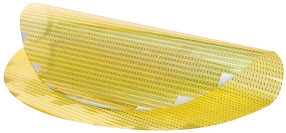
PlasticARM flexible chip
Source: PragmatIC.
It uses flexible components, and unlike silicon-based chips, it can be printed on curved surfaces without degradation such as plastic, paper, and other inexpensive materials. This will create a true Internet of Everything. Arm said that in the next ten years, chips will be integrated into “more than one trillion inanimate objects.”
PragmatIC
I’d like to introduce PragmatIC into the discussion.
The chip was designed in collaboration with flexible electronics manufacturer PragmatIC, and as the company’s designers explained in a paper published in the journal Nature, it does not yet have the same features as silicon-based chip designs. For example, it can only run three test procedures that are hard-wired into its circuit during the manufacturing process. Arm researchers stated that they are working on a future version that will allow the installation of new code.
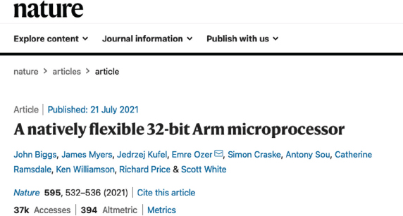
A natively flexible 32-bit Arm microprocessor
Source: Nature magazine.
PragmatIC Technical Advantages
PragmatIC provides a unique technology platform to create ultra-low-cost flexible integrated circuits (FlexIC). Its FlexIC Foundry service enables chip designers to create their own application-specific flexible devices at a fraction of the cost and time required to develop traditional silicon ICs. Innovators can use its foundry products to iterate and test concepts within a few weeks, thus greatly speeding up the development cycle. Its thin, flexible, and robust FlexIC can be easily integrated with other thin-film electronic components to create novel solutions. FlexIC is manufactured on its revolutionary FlexLogIC production system, which is a highly scalable manufacturing model that enables cost-effective mass production.
Compared with traditional silicon IC fabs, the capital investment and operating costs have been reduced by several orders of magnitude. PragmatIC also provides ready-made FlexIC. Its ConnectIC series extends proven applications such as radio-frequency identification (RFID) and Near-field communication (NFC) to mass market use cases, enabling trillions of smart objects that can interact with consumers and their environment.
PragmatIC was established in 2010 and is headquartered in Cambridge, England. It has raised US$65.9 million and has its first billion-unit production facility in Sedgefield, UK. Shareholders include Cambridge Innovation Capital, Arm, and Avery Dennison. The founders of PragmatIC include the following.
Scott White, Cofounder and CEO
Cofounder Scott White is an experienced serial entrepreneur and now leads his sixth technology venture as the CEO of PragmatIC. He is also a director of Cortexica Vision Systems, a mobile visual search company. Past successes include Azea Networks. Azea Networks provides world-class submarine optical network solutions. It developed from a concept to an eight-figure sales level before it was acquired by Xtera. Scott also has an international perspective. He has lived and worked in many countries, including Australia, Japan, Singapore, Indonesia, the United States, and the UK.
Richard Price, Chief Technology Officer and Cofounder
Richard has more than 20 years of experience in technology commercialization, focusing on printed electronics and materials chemistry. He was a senior chemist at Elam-T and discovered 100 new materials. He is the co-inventor of seven patent families. Richard also served as the venture capital manager of Manchester University Intellectual Property Ltd. He led the creation of spin-off companies, including CableSense, Arvia Technology, and Nano ePrint.
Cofounders, Richard Price (left) and Scott White (right)
Source: PragmatIC.
Video version (www.youtube.com/watch?v=E8rfeaoVUvc).
Which Material Chip Can Replace Silicon-Based Chips
In order to break through the limitations of Moore’s law on the performance of silicon-based chips, in fact, many traditional semiconductor companies have been actively developing new materials.
One of these materials is gallium nitride (GaN), which is a compound semiconductor formed by combining gallium and nitrogen into crystals.
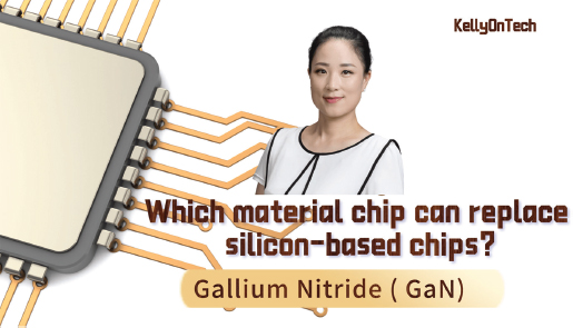
Gallium nitride (GaN). Which material chip can replace silicon-based chips?
Why Choose This Material?
This material is very suitable for high-power, high-efficiency, and high-temperature electronic applications. The electron mobility of GaN semiconductors is 1,000 times that of silicon—they flow faster. Compared with silicon-based chips:
• The power consumption of GaN chips is a quarter of that of silicon-based chips.
• The size is a quarter of the silicon-based chip.
• The weight is a quarter of the silicon-based chip.
• GaN chip solutions are cheaper than silicon-based solutions.
• If GaN chips are used in the data center, it means higher revenue per rack and more energy saving.
• If it is used in a renewable energy system, it means that more electricity can be stored and converted.
• If it is used in an electric car, it means that the mileage on a single charge is longer.
• If used in consumer devices, it means high-speed wireless charging.
Whether Gallium Nitride Is Expensive as a Raw Material?
GaN is more expensive than silicon, which is the most abundant element on the earth after oxygen. But one company has already managed to reduce the overall system cost by 20 percent to make up for this.
Which Company Produces GaN Chips?
This company is GaN Systems, established in 2008 in Kanata, a suburb of Ottawa, the capital of Canada. Investment institutions include BDC Capital, Commercial Development Bank of Canada (the National Development Bank wholly-owned by the Canadian government). By the way, Cycle Capital Management is Canada’s most influential and largest clean technology private equity fund. It also has an office in Qingdao, China. It is committed to commercializing clean technology. BMW iVentures has also made a strategic investment in GaN Systems.
Founding Team of GaN Systems
Girvan Patterson, the cofounder and first CEO of GaN Systems, is a chartered electrical engineer with nearly 40 years of experience in the field of telecommunications and data networking. He used to work in Bell Laboratories and is very authoritative in the field of computer-aided design (CAD) system development and holds patents. Girvan once founded Orcatech Inc., a graphics workstation manufacturer, and cofounded Plain-tree Systems Inc., a pioneer in Ethernet switching. Girvan has completed four initial public offerings (IPOs) on the Toronto Stock Exchange and Nasdaq, and has 20 years of experience on the board of public companies.
Girvan Patterson, the cofounder and first CEO of GaN Systems
Source: Ottawa Business Journal.
The other cofounder is John Roberts, who has rich experience in the semiconductor field and deep network resources. He had founded two semiconductor companies based in Ottawa, Calmos (later Tundra) Semiconductor and SiGe Semiconductor. As early as 1989, he became the CEO of the Strategic Microelectronics Alliance, which is composed of 25 semiconductor companies, including IBM and Nortel.
John Roberts, the cofounder of GaN systems
Source: The Globe and Mail.
What Are the Practical Applications of Gallium Nitride Chips?
GaN chips have been used by more than 2,000 companies. Let me take electric vehicles as an example: GaN is becoming the technology of choice for power conversion and battery charging in hybrid and electric vehicles.
• GaN chips are used in LiDAR, which can increase the performance of LiDAR by 10 times, providing four channels of laser and higher resolution.
• In addition, the GaN chip is used for in-vehicle wireless charging, and its functions are also very powerful. It supports fast charging of multiple mobile phones at the same time. The mobile phones can be placed at will. There is no specific location requirement. The charging is completely free from interference from other items.
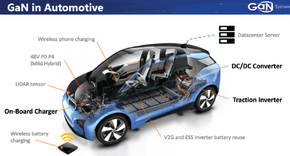
GaN in automotive
Source: GaN Systems.
The Jaguar I-PACE pure battery electric vehicle with the agility of a sports car also uses chips provided by GaN Systems.

The Jaguar I-PACE pure battery electric vehicle
Source: Jaguar.
GaN chips have also been used in many other fields, such as:
• Consumer electronics
• Data center server
• Solar inverters
• Car battery charger for EV/HEV
Where Can I Buy GaN Chips?
GaN Systems sells mainly through its cooperative distributors around the world.
One of the distributors is Mouser Electronics. Mouser Electronics is a global distributor of the semiconductor and electronic components industry. The original factory authorizes the distribution of more than 1,100 brand manufacturers, and can order more than five million products online, providing a one-stop procurement platform for design engineers and purchasers.
Another distributor is Richardson Electronics (NASDAQ: RELL), which sold its RF Wireless and Power Division (RFPD) to Arrow Electronics (NYSE: ARW) in March 2011.
Video version (www.youtube.com/watch?v=F2e28oRrK7w).
What Are the Latest Developments in Chip Processing Technology
What Is the Most Valuable Asset Recognized Globally in the 21st Century?
It is data. At present, the data exchange between man–machine and machine–machine channels consumes about 9 percent of the world’s energy, and it is increasing at a rate of 20 to 30 percent every year. Moreover, the deployment of faster data networks and the IoT is increasing.
What are the latest developments in chip processing technology? Versics
In this continuously connected world, data traffic has approached the bandwidth limit of communication networks, and high-speed optical communication is urgently needed.
Plasma Chips
Researchers at the Swiss Federal Institute of Technology Zurich have been working on a chip for nearly 20 years. On this chip, fast electronic signals can be directly converted into ultra-fast optical signals, with almost no signal quality loss.
By the way, this project is part of the European Horizon 2020 research project. This chip will greatly improve the efficiency of optical communication infrastructures (such as optical fiber networks) that use light to transmit data.
In the past, researchers have tried a method called overall collaborative integration. Simply put, it is to put the electronic chip and the photonic chip in layers and press them as tightly as possible to shorten the path and reduce the loss of signal quality. However, the monolithic method failed because the size of the photonic chip is much larger than that of the electronic chip, and it is impossible to combine them on the same chip.
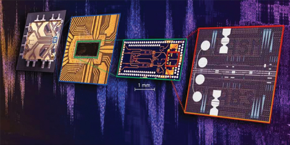
Plasma chips
Source: ETH Zurich/Nature Electronics.
In 2019, researchers at ETH Zurich overcame the size difference between photonics and electronics by replacing photonics with plasma. As plasma chips are smaller than electronic chips, they can actually be manufactured more compactly.
Versics
Here I introduce a start-up company—Versics. It is led by Marc Reig Escalé, a physicist at the Institute of Quantum Electronics at ETH Zurich. Versics is his innovative project as an ETH Pioneer Fellowship. Versics is the abbreviation of multifunctional optics. The technology has many applications and can also be used for satellite communications in the future.
We know that fiber optic cables are only half of the world of data traffic. The information needs to be encoded and decoded. This means that it must be written into the optical signal and then read again at the end.

Marc Reig Escalé, a physicist at the Institute of Quantum Electronics at ETH Zurich
Source: ETH Zurich.
Marc Reig Escalé and his colleagues found a way to write this information more efficiently than before. They chose the best materials in the fields of optics and microelectronics to manufacture microchips.
The first is silicon, which is the most important material in the computer industry. As a semiconductor, it is very suitable for building circuits, such as circuits on computer and mobile phone chips. In crystalline form, silicon is also used in optical chips to transmit light waves. This has practical advantages because the manufacture of micro-formats is already very mature in the field of microelectronics.
However, for optical purposes, silicon is far from the best choice. Lithium niobate offers more advantageous properties: for example, it can work in a wider range of optical frequencies. An important attribute of data processing is that this crystalline material can change the intensity of incident light according to an externally applied voltage. This allows electrical signals to be converted into optical signals.
This chip consumes less energy and processes signals at least twice as fast as commercial alternatives currently in existence.
Video version (www.youtube.com/watch?v=L7jXPLnI_i0).
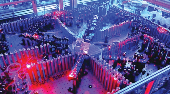
What Are the Latest Developments of Quantum Chips?
What Is Quantum Supremacy?
We have listened to quantum hegemony many times. According to Wikipedia, in quantum computing, it is proved that programmable quantum devices can solve problems that classical computers cannot solve in any feasible time.

What is the latest development of quantum chips?
How Can Quantum Supremacy Be Achieved?
In classical computing, information is coded in bits. In quantum computing, information is encoded in qubits or quantum bits. Qubits can be expressed as two states corresponding to classical computing 0 or 1 or a quantum superposition of the two states at the same time.
The unique superposition state can enable quantum computers to solve problems that are almost impossible to solve by classical computers, and it is likely to promote breakthroughs in application fields such as material design, drug discovery, and machine learning.
How Can It Be Calculated Faster?
Simply put, it is to increase the number of qubits, just like a child counting 1 to 10 is using 10 fingers. If counting 1 to 20, they can use both fingers and toes. It’s easy to say, but it’s difficult to implement. Because qubits are very unstable, quantum chips need to operate in an extreme temperature environment of –273°C to protect the qubits from external shocks. In order to work, according to Google’s standards, the error rate for every two qubits needs to be less than 0.5 percent.
Delft University of Technology
Therefore, some research institutions seek breakthroughs in manufacturing processes. Here I would like to introduce Delft University of Technology (TU Delft) in the Netherlands. Their researchers and Intel’s research laboratory have introduced nanotechnology and fabricated nanoscale silicon transistors. The most critical breakthrough was that they have achieved this by using industrial chip manufacturing processes. This means that the output is high enough to enable industrial-scale manufacturing of quantum computing chips.
By the way, the Dutch government is now building a 12,000 sq. m national headquarters for quantum research called the Quantum House, which is located on the campus of the Delft University of Technology and is expected to be completed in 2024. This project will also participate in the European Commission’s design of the future European Quantum Communication Infrastructure Network (EuroQCI).
Circuit-Based Quantum Chips
At present, the technical routes of global quantum chips are not the same. Companies such as Google, IBM, and Intel Corporation mainly study superconducting quantum computing, which is an implementation of quantum computers in superconducting electronic circuits. For example, the Bristlecone quantum chip launched by Google in 2018 has 72 qubits.
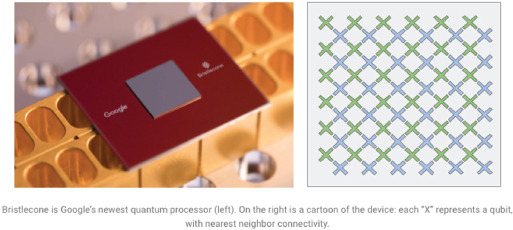
The Bristlecone quantum chip
Source: Google.
The University of Science and Technology of China’s quantum computing research is based on photons, and has developed the world’s first photonic quantum computer to achieve quantum hegemony.
Jiuzhang Photonic Quantum Computers
Source: The University of Science and Technology of China.
On December 3, 2020, the University of Science and Technology of China announced in the Science magazine that its photonic quantum computer named Jiuzhang successfully sampled the Gaussian boson within 200 seconds and detected up to 76 photons. The University of Science and Technology of China estimates that it will take 2.5 billion years for the Sunway TaihuLight supercomputer to complete the same calculation.
Annealed Quantum Chip
The company D-Wave Systems has provided commercial quantum computers for large companies such as the U.S. military and Volkswagen, which uses different technologies. For the specific introduction of this company, you can refer to the video (www.youtube.com/watch?v=jMzRPpHXvGk) I posted before.
D-Wave uses annealing quantum computing, mainly to solve optimization problems. In 2011, D-Wave developed the world’s first commercial quantum computer with 128 qubits, with a price of approximately US$10 million. The D-Wave Advantage launched in 2020 has 5,760 qubits.
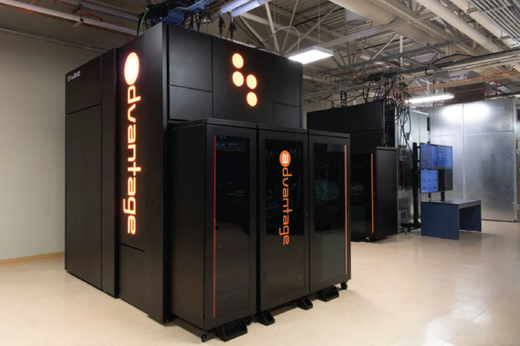
Annealed quantum chip
Source: D-Wave Systems.
Another company researching quantum annealing is Japan’s NEC, which has been conducting quantum technology R&D since the 1990s and successfully constructed the world’s first solid qubit. NEC recently reached a cooperation agreement with ParityQC, a quantum architecture start-up in Austria that was only established in 2020. The company uses the proprietary quantum operating system ParityOS to develop and design quantum computers for customers, mainly for optimization problems.
Video version (www.youtube.com/watch?v=3SO0pjiuFd0).
The Latest Developments in Artificial Intelligence Chips
What Is an Artificial Intelligence Chip?
According to Wikipedia, AI accelerators are a type of specialized hardware accelerators or computer systems designed to accelerate artificial intelligence (AI) and machine learning applications, including artificial neural networks and computer vision.
Typical applications include robotics algorithms, the IoT, and other data-intensive or sensor-driven tasks. They are typically multicore designs, often focused on low-precision arithmetic, novel data flow architectures, or in-memory computing power.
As of 2018, the typical AI integrated circuit chip contains billions of MOSFET transistors (the metal–oxide–semiconductor field-effect transistors). Many vendor-specific terms exist for such devices, and it is an emerging technology without a dominant design.
The latest developments in AI chips
The growth of the global AI chip market is mainly driven by the increasing demand for smart homes, the development of smart cities, and the emergence of quantum computing. In the near future, more and more countries will adopt AI chips to develop smarter robots.
Video version (www.youtube.com/watch?v=HcHMc906Is0).
Which Company Is the Global Leader in AI Chips?
It is Cambricon Technology Corporation, established in 2016. It is engaged in the design and sales of AI core chips in various cloud servers, edge computing devices, and terminal devices, providing customers with a wealth of chip products and system software solutions.
In May 2018, Cambricon released its third-generation AI chip for edge devices with the help of TSMC’s (Taiwan Semiconductor Manufacturing Company) 7 nm process.1 Moreover, the company aims to have one billion smart devices that are expected to use its AI processors.
On January 21, 2021, Cambricon’s SiYuan 290 smart chip and accelerator card and the Xuansi 1000 smart accelerator were officially unveiled for the first time after mass production.
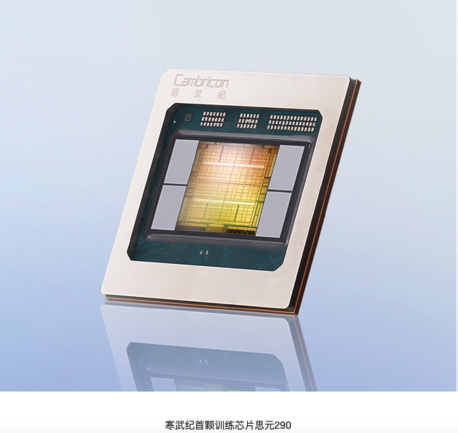
The SiYuan 290 AI chip
Source: Cambricon.
The SiYuan 290 AI chip is Cambricon’s first training chip, using TSMC’s 7 nm advanced process, integrating 46 billion transistors, supporting MLUv02 extended architecture, and fully supporting AI training, inference or hybrid AI computing acceleration tasks.
We know that graphics processing units (GPUs) have led the AI chip market since 2018, used to process images and solve most parallel computing problems, such as Bitcoin mining. But in the future, application-specific integrated circuit (ASIC)-dedicated integrated circuits, also called ASIC custom chips, will overtake GPUs in terms of revenue. (A dedicated integrated circuit is an integrated circuit chip that is customized for a specific application, not for general purpose use. For example, a chip designed to run in a digital recorder or efficient bitcoin miner is an ASIC.)
Google TPU
The most famous ASIC custom chip is the familiar Google Tensor Processing Units (TPUs). At the 2021 I/O Developers Conference, Google announced its fourth-generation TPU AI chip. Google said its speed is twice that of the previous version launched in 2018.
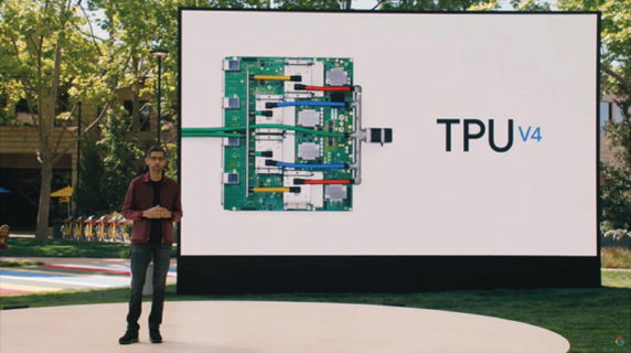
TPU V4
Source: Google.
As Google CEO Sundar Pichai pointed out, these chips will then be combined with 4,096 v4 TPUs in pods. A single pod provides more than one exaflop of computing power. Is that not much of an idea? Google claims that if there are about 10 million laptops all working together in the world, then it can be almost comparable to a single pod in terms of power.
Video version (www.youtube.com/watch?v=qEwdgdBHzgk).
Which Artificial Intelligence Chip Start-Up Is Worth Watching?
I will introduce an AI chip start-up Tenstorrent, touted by the industry as having the most promising architecture on track to become the next generation of computing giants.
Founded in 2016 in Toronto, Canada, Tenstorrent is the world’s first chip company to design a conditional execution architecture for facilitating scalable deep learning. Its flagship product is GraysKull.
Tenstorrent takes an approach that dynamically eliminates unnecessary calculations, thus breaking the direct link between the growth of model size and the calculation/memory bandwidth requirements. Conditional calculations make it possible to adapt the model’s inference and training to the precise input proposed, such as adjusting the NLP model calculations to the exact length of the presented text, and the dynamic trimming of the model based on input features. Grayskull provides significant baseline performance improvements in today’s most widely used machine learning models, such as BERT, Resnet-50, and other machines while using conditional execution to open up order-of-magnitude gains during conditional execution of the current model and future executions optimized for this method.
In May 2021, Tenstorrent raised $200 million in a new round of financing from investment institutions led by Fidelity Management, including Eclipse Ventures, Epic CG, and Moore Capital. The deal is valued at US$1 billion and also makes Tenstorrent a unicorn company for AI chips.
The Founding Team of Tenstorrent
Ljubisa Bajic, cofounder and CEO of Tenstorrent, has been designing chips at AMD for more than a decade. Bajic also worked at Nvidia.

Cofounders of Tenstorrent, Jim Keller (left) and Ljubisa Bajic (right)
Source: Tenstorrent.
When designing AMD’s now very successful Zen architecture in 2014, he met Jim Keller, a star chip designer invited by AMD. Keller has designed breakthrough chips at Apple and Tesla.
Bajic also successfully persuaded Keller to resign as Intel’s senior vice president in June 2020 and join Tenstorrent as president and chief technology officer. With this industry powerhouse on board, Tenstorrent has set a goal: to develop chips for training machine learning programs, surpassing the current global design.
The company’s strategy is to use software to better allocate the use of computing power on each chip. Gossip here, in fact, Bajic founded Tenstorrent with the encouragement of Keller who provided seed funds for the company. Tenstorrent also focuses on developing a different way to link its many chips so that they can share data faster than standard products. Instead of connecting to each other via external networking technologies such as Ethernet, these chips can communicate more directly with each other.
AI Chip Market Outlook
According to IDC, a leading global market intelligence firm, the dedicated AI chip market reached nearly $15 billion in hardware in 2020, led by Nvidia, and is expected to grow by 20 percent annually to $31 billion by 2024.
Recently, Baidu launched the second-generation AI chip Kunlun 2 for autonomous driving and other fields.
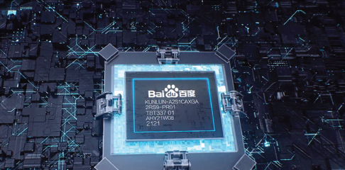
Kunlun A2S1CAXGA chip
Source: Baidu.
Baidu also released a prototype of the robot car, highlighting its ambitions in autonomous driving.
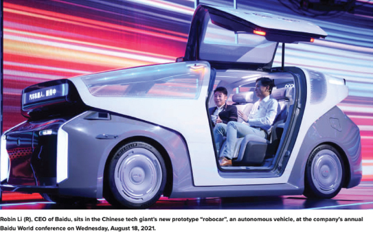
Baidu’s new prototype robocar
Source: Baidu.
Video version (www.youtube.com/watch?v=k9wDHHyRAIQ).
Why Can SambaNova Systems, an AI Chip Start-Up, Become One of the 10 Unicorn Companies?
Sambanova Systems is known as one of the top 10 unicorn companies in the United States. (A unicorn company is a privately held start-up company valued at over 1 billion U.S. dollars.) SambaNova Systems raised 678 million U.S. dollars in Series D venture capital through a transaction led by Soft-Bank Investment Advisers in April 2021. The previous rounds of investment institutions include Google Ventures, BlackRock, Intel Capital, Samsung Catalyst fund, and SK Telecom, a total of 12 investment institutions.
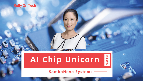
AI chip unicorn: SambaNova systems
This company was founded in 2017 in Palo Alto, California, United States. It became a unicorn company in February 2020. It is also rated as the AI chip start-up company that has received the most investment in the world in 2021. Most of its customers are national laboratories, such as Lawrence Livermore National Laboratory and Argonne National Laboratory.
What Are the Current Problems With AI Chips?
According to Intel’s analysis, the biggest challenge currently facing AI chips is bandwidth. As the content of neural network models grows exponentially, the on-die memory of any AI chip must scale accordingly.
For example, Openai’s recently released GPT-3 deep learning language model has 175 billion parameters. Although in-depth learning accelerators have a lot of hype in the market, their utilization rate is extremely low, because the engineering team has been busy moving parameter data on the network, because 100 billion parameters are no longer suitable.
So Intel’s team of engineers evaluates how to optimize bandwidth, cache, actually depending on how to optimize the amount of data movement that needs to be performed. I/O may become a very big bottleneck for AI chips. Intel has specially set up a project team for connection problems, which is run by Vice President Hong Hou.
Another challenge is called Sparsity, which refers to the fact that most of the values in a vector in vector-matrix operations are null. This causes GPUs to waste a lot of energy because they cannot separate zero-valued items to fit the GPU’s memory layout when they batch many vectors. Sparsity is a work in progress.
Raja Koduri, Intel’s chief chip architect, predicts that AI will lead to a revolution in chip architecture.
Why Was SambaNova Systems Favored by These Investment Institutions?
First of all, its cofounders are very talented. They include:
1. Dr. Kunle Olukotun, known as the father of multi-core processors, is the Cadence design system professor at Stanford University’s School of Engineering, Stanford University’s electrical engineering and computer science professor, and the head of the Stanford University Universal Parallel Laboratory.
2. Chris Re, a professor at Stanford University and a computer scientist, focuses on big data analysis. He won the MacArthur Genius Award in 2015.
3. Rodrigo Liang is the CEO and cofounder of SambaNova Systems. Before joining SambaNova, Rodrigo was responsible for Oracle’s SPARC processor and ASIC development. He led the engineering project team responsible for designing the latest processors and ASICs for Oracle Enterprise Server.
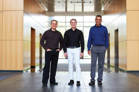
Cofounders of SambaNova Systems: Dr. Kunle Olukotun, Rodrigo Liang, and Chris Re (from left to right)
Source: SambaNova Systems.
Strategic Positioning of SambaNova Systems
Second, let’s take a look at the strategic positioning of Sambanova Systems.
This company has focused on high-value areas in the field of AI since its inception, including natural language processing (NLP) and absolute computer vision. Customers in these fields need large-scale rapid acceleration in order to avoid shredding data and images to force adaptation. If a better memory balance can be found, these customers can also consider giving up the GPUs.
SambaNova Systems positions itself as a developer of advanced system platforms and hardware, specializing in providing support for machine learning and data analysis. It provides a flexible, scalable, and optimized system architecture for data flow, allowing manufacturers to use AI-based hardware to create faster and more efficient algorithms. In this way, the client companies will not seriously delay the progress of any project because of the need to train the company’s data science team and other teams.
They developed what is known as the pioneer magic box of AI, including the device-based DataScale system and the subscription-based data as a service (DaaS) platform. The whole concept is to put all the content of model optimization and deployment as back-end processing without end user involvement.
The Competitive Advantages of SambaNova Systems
SambaNova Systems’ most significant application is in computer vision, especially in the fields of medical imaging, and it is currently the best tool for handling a large number of voice and image workloads. Their device can handle a resolution of 50 k × 50 k, which makes SambaNova particularly feasible when processing entire image slides without loss of quality or data.
Its main target markets include e-commerce recommendations, health care, energy, and banking that use NLP and high-resolution image processing.
Video version (www.youtube.com/watch?v=Owi7h9BEoWo).
Bionic Chips: Qualcomm and Apple Fight a Chip War
What Are Bionic Chips?
Bionic chips are also known as multicore system chips and are mainly designed to save battery life. I use Apple’s bionic chips as an example. Apple has used bionic chips in all of its phones since the iPhone 8. The Bionic chip has four high-efficiency cores and two high-performance cores. Most of the time, the high-efficiency cores are used. However, high-performance cores are used when process-intensive tasks such as video playback are activated.
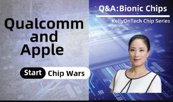
Q&A: Bionic Chips
The iPhone 13 series is equipped with the A15 bionic chip developed by Apple. It adopts the industry’s most advanced 5 nm process technology and integrates 15 billion transistors. They have also improved the performance of the machine learning accelerator in the CPU. Apple said that it is the fastest CPU in a smartphone with 50 percent faster graphics processing for all types of machine learning tasks, and can perform 15.8 trillion operations per second, up from 11 trillion per second in the A14.
Why Develop Bionic Chips?
This brings us to the combination of trends in the computing industry. There has been an explosion in data and, in turn, an explosion in the data centers required to store all this information. Humans have no way to process so much information, so we use machines to do so. Therefore, our need for complex machine learning algorithms has grown exponentially. But, as Moore’s law slows down, the growth in computing power can’t keep up with our needs.
Let’s talk about the trend of the chip industry. In order to reduce the dependence on traditional chip manufacturers (such as Qualcomm, AMD, Intel, etc.) as early as more than a decade ago, major companies like Amazon, Google, Facebook, and so on began to establish their own chip teams and design their own proprietary chips. The Arm architecture is generally used.
How Do Traditional Chip Giants Respond?
I use Qualcomm as an example. In March 2021, Qualcomm spent $1.4 billion to acquire Nuvia, a two-year-old chip start-up. One of the reasons was because of Nuvia’s strong team, known as the iron triangle of the chip industry.
The Founding Team of Nuvia
In 2019, Nuvia was founded in Santa Clara, California, by three former Apple engineers.
• Gerard Williams III—Cofounder and CEO, Nuvia, Senior Vice President of Engineering at Qualcomm. Gerard previously spent 12 years at ARM and nine years at Apple as the lead architect for custom processors for the iPhone and iPad.
• John Bruno—Cofounder, Nuvia, VP of Engineering at Qualcomm. John is an excellent system architect. He worked at AMD for eight years, Apple for five years, Google for one year and four months, delivering the most important IT part of the chip, the CPU.
• Manu Gulati is a great SOC micro-architect. He used to work at Apple for seven years, Google for one year and 11 months. His job was to put the chips together. In addition, he is very familiar with mobile hardware.
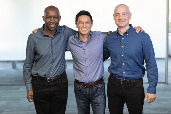
Cofounders of Nuvia: John Bruno, Gerard Williams III and Manu Gulati (from left to right)
Source: Nuvia.
Although all three founders have backgrounds in mobile chipsets, they started Nuvia with other ideas. Nuvia has always been secretive and rarely discloses its R&D progress. Their main focus is on solving the conceptual data center (i.e., cloud computing) and finding more energy-efficient ways to deal with the rising costs and environmental and climate impacts of machine learning workflows and compute-intensive processing.
Nuvia’s investors not only have a deep technical background, but also have strong financial resources. These include Capricorn Investment Group. The fund focuses on investing in technology companies that have a positive impact on the world, and its portfolio includes Tesla and Planet Labs. Other investors include Dell Technologies Capital (DTC) and Mayfield.
Apple Sued Gerard Williams
Apple sued Nuvia cofounder Gerard Williams for using his work time to conceive Nuvia and convince other Apple employees to leave the company and join Nuvia while he was at Apple. The Santa Clara County Superior Court accepted the petition. Of course, Gerard also filed a countersuit against Apple, stating that Apple illegally monitored his text messages while he was working there. And the chips later developed at Nuvia were targeted at data centers.
Why Did Qualcomm Buy Nuvia?
In addition to the strong founding team, Qualcomm acquired Nuvia in order to lay out 5G, further accelerate the convergence of mobile and computing on top of its own Snapdragon technology, and create a new high-performance computing platform.
Video version (www.youtube.com/watch?v=WYQsCaQccN4).