
S
saponification Reaction converting rosin into rosin soap. Post-soldering cleaning processes that allow water to be used as a cleaner as opposed to as a solvent.
saponifier A generic term for an aqueous solution of organic or inorganic bases and various additives for promoting the removal of rosin and sometimes water soluble fluxes. The removal of rosin-based fluxes is based on a chemical reaction between rosin acids and a base in the saponifier, rendering it soluble and/or dispersible in detergent solution as the rosin “soap.”
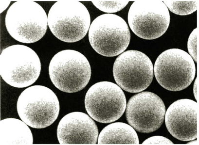
saturated solution A solution in which the solvent can accept no more solute. The result of adding additional solute to the solution is the formation of the solute as a distinct phase, e.g., solid particles suspended or precipitated to the bottom of the container in which the solution is held.
scan rate The pace at which a machine scans the surface of a unit, such as a solder joint, to determine volume. Expressed as surface area per unit of time.
scavenged air Air removed from appropriate parts of the process area, i.e., tunnels, to ensure there are no fluid or gas vapors in the work place.
scavenging In soldering, the dissolving (alloying) of the material to be soldered into the molten solder. Also known as leaching.
schematic diagram A drawing showing, by means of graphic symbols, the electrical connections, components, and functions of a specific circuit arrangement.
screen A network of metal or fabric strands, mounted snugly on a frame, upon which the film circuit patterns and configurations are superimposed by photographic means.
screen printing A process for transferring an image to a surface by forcing suitable media through a stencil screen with a squeegee. Also called silk screening.
screening The process whereby the desired film circuit patterns and configurations are transferred to the surface of the substrate during manufacture by forcing a material through the open areas of the screen using the wiping action of a soft squeegee.
secondary side In through-hole technology, this term refers to the soldered side of the PCB. In surface mount technology, this term refers to the secondary side, which typically is limited to passive chip components. Also known as solder side.
seeding Process in electroless copper deposition where the sensitized board is dipped into an acidic solution of palladium chloride.
selective etch Restricting the etching action on a pattern by the use of selective chemicals that attack only one of the exposed materials.
self-align Design of two mating pairs so that they will engage in the proper relative position.
semi-additive process An additive process for obtaining conductive patterns that combines an electroless metal deposition on an unclad substrate with electroplating or etching, or with both.
semi-aqueous cleaning This cleaning technique involves a solvent cleaning step, hot water rinses, and a drying cycle.
semiconductor device Any device based on either preferred conduction through a solid in one direction, as in rectifiers; or on a variation in conduction characteristic through a partially conductive material, as in a transistor.
sensitize Process in electroless copper deposition where the board is dipped into acidic stannous solution.
service loop A small portion of wire or conductor that is added to the overall length to facilitate maintenance and further servicing.
shadowing (1) A condition in infrared reflow soldering in which component bodies block the direct infrared energy from certain areas of the PCB, possibly resulting in insufficient temperatures to completely melt the solder paste. (2) In wave soldering, it refers to solder failing to wet the surface mount device leads due to another device blocking the solder flow. Also known as shadow effect.
shelf life The length of time under specified conditions that a stored material in original, unopened containers retains its usability. Also called storage life.
silicon A brittle, gray, crystalline chemical element that, in its pure state, serves as a semiconductor substrate in microelectronics.
silicone A group of semi-organic polymers that have good heat stability and are water repellent. In soldering they are considered a poison to the joining process, because of their tenacity. Silicone oil, for instance, cannot be totally cleaned off a surface with electronic grade solvents.
silk screen A screen of a closely woven silk mesh stretched over a frame and used to hold an emulsion outlining a circuit pattern and used in screen printing of film circuits. Used generically to describe any screen (stainless steel or nylon) used for screen printing.
silver chromate paper test A simple qualitative test to determine the presence of ionic halides. Usually used to check that a mildly activated flux, such as type RMA, contains no ionic halides. The Silver Nitrite Test, which is another method, serves the same purpose.
silver migration Silver is a metal prone to electromigration in which the migration can extend along the surface and tends to follow paths through fibrous materials along the surfaces.
silver nitrate test A simple qualitative test to determine the presence of ionic halides. The Silver Chromate Paper Test, which is another method, serves the same purpose.
simulate A software model that predicts a board’s operation before it is built.
simultaneous placement Placement of more than one surface-mounted component onto a circuit board at one time.
single in-line package (SIP) An assembly consisting of two or more surface mount components mounted on a common substrate. The components are interconnected to each other and to pins at the substrate edge for through-hole mounting on a PCB.
single wave soldering Wave soldering process using just one solder wave.
skew Describes the misalignment of a part to its target.
slump A spreading of material (solder paste, conductive adhesive, thick film composition, etc.) after screen or stencil printing but before reflow soldering, curing, or drying. Too much slump results in a loss of definition.
small outline integrated package (SOIC) A package in which an integrated circuit chip can be mounted to form a surface mounted component. It is made of a plastic material that can withstand high temperatures and has leads formed in a gull-wing shape along its two longer sides for connection to a PCB footprint.
SMTA Surface Mount Technology Association
snap-back The return to normal of a stencil after being deflected by the squeegee moving across the surface of stencil and substrate.
snap-off distance The height the stencil is set above the board for an “off-contact” printing, which determines the amount of deflection that occurs during the snap-back action of the stencil. Snap-off distance is typically in the range of 0.003 to 0.050″. On-contact printing would have a zero snap-off distance.
soak Period of time after preheat and before the reflow spike where the internal temperature differences between components are allowed to equalize. Also known as drying time, preflow, and stabilization period.
soft solder A low-melting solder, generally a lead-tin alloy, with a melting point below 600°F.
soft water Processed water where the hardness has been replaced with sodium ions. This grade of water is suitable for most electronic cleaning applications and is more economical than de-ionized (DI) grade water.
soils Foreign matter that might exist on a surface to be soldered, possibly interfering with the soldering process. It may be organic or inorganic.
solder (1) An alloy that melts at relatively low temperatures, and which is used to join or seal metals with higher melting points. Solder alloys melt over a range of temperatures; the temperature at which a solder begins to melt is the solidus, and the temperature at which it is completely molten is the liquidus. (2) A metal alloy, usually having a low melting point, used to join other metals having higher melting points than the solder. Solder is an adhesive; it wets the surfaces and forms the joint by causing molecular attraction between the solder and base metal. It also may diffuse the solder metal or alloy into the base metals or vice versa. Solders are generally classified as soft solders and hard solders. Soft solders have melting points up to approximately 600°F, whereas the melting points of the hard solders are above 1100°F. The most common examples of soft solders are the tin-lead alloys.
solder balls Very small balls of solder that separate from the main body of solder which forms the joint. Primarily caused by excessive oxides in the solder paste that inhibit solder coalescence during reflow.
solder bump Solder spheres bonded to contact areas or pads of devices and used for face-down bonding.
solder cream Another term for solder paste. It is a homogeneous combination of solder, flux, solvent, and a suspension agent for automated production of solder joints. Available with a variety of flux bases.
solder dam A dielectric composition screened across a conductor to limit molten solder from spreading further onto solderable conductors.
solder foil Solder alloys in the form of thin tape in various widths, typically ranging from ¼ to 3″. Also called solder tape or solder strip.
solder fusion equipment, IR Systems that change the porous, electroplated tin-lead on a circuit into an alloy with a strong bond to the base copper. Conveyorized infrared fusing systems fuse both sides of a double-sided board simultaneously. They consist of a fluid application stage for applying fusing fluid, a preheat zone, a fusing zone, and a cooling zone.
solder leveling The process of dipping PCBs into hot liquids, or exposing them to liquid waves to achieve fusion. First, flux is applied to the board by dipping or brushing. Then the board is preheated in a liquid maintained at 250°F. Next, the board is immersed in fusing liquid of 430°-500°F. Finally, it is dipped in another 250°F liquid to cool it and reduce thermal shock. Thin fused coatings can be applied.
solder marks A screening defect that is characterized by a print having jagged edges. This condition is a result of incorrect dynamic printing pressure or insufficient emulsion thickness.
solder mask A PCB technique where everything is covered with a plastic coating except the contacts to be soldered.
solder mask over bare copper (SMOBC) A printed wiring technology that protects bare copper conductors with solder mask exposing only the component land patterns.
solder pallets PCB holders on conveyors to the wave-solder or reflow system that are used continuously from the assembly area to eliminate excessive handling.
solder paste A homogeneous combination of solder powder, flux, solvent, and a gellin or suspension agent for automated production of solder joints. Available with a variety of flux bases.
solder preforms Manufactured solder configurations containing a predetermined quantity of alloy, with or without a flux core or coating. Available as stamped washers, spheres, and formed wire.
solder resist Permanent or temporary coatings that mask off and surface insulate those areas of a circuit where soldering is not desired or required.
solder side In through-hole technology, this term refers to the soldered side of the PCB. In surface mount technology, this terms refers to the secondary side, which typically is limited to passive chip components. Also known as secondary side.
solder skip Joint not properly soldered due to shadowing by one or more component bodies as an assembly is wave soldered.
solder strip Solder alloys in the form of thin tape in various widths, typically ranging from ¼ to 3″. Also called solder foil or solder tape.
solder tapes Solder alloys in the form of thin tape in various widths, typically ranging from ¼ to 3″. Also called solder foil or solder strip.
solder voids Emission of gas or air from a printed circuit board or joint as the board is soldered.
solder wicking A condition whereby solder on the terminal of a surface mounted component being soldered migrates up from the circuit board land and leaves insufficient solder on the land to give a good joint.
solderability (1) The ability of a conductor to be wetted by solder and to form a strong bond with the solder. (2) A qualitative measure of the ability of PCB pads or of a component’s leads or terminations to be completely wetted by molten solder.
solderability testing There are several test systems presently in use for both PCBs and components. An additional test can be used for plated-through holes and components. They are: (1) the edge dip solderability test, (2) the meniscus test, and (3) the globule test. In addition to these, any test, mutually agreed to by vendor and customer for the solderability of components including printed circuit boards, is acceptable.
soldering The process of joining metals by fusion and solidification of an adherent alloy having a melting point below about 800°F.
soldering, reflow A process in which solder paste is deposited upon pre-tinned pads on a PCB and the component’s pre-tinned leads are placed upon the paste. When the assembly is heated to the proper temperature, the solder paste melts and the solder on the leads and pads reflows to form a solder fillet.
soldering, vapor phase reflow A type of reflow soldering in which the PCB assembly is passed through a vaporized inert fluorocarbon. The latent heat given up when the fluorocarbon condenses causes the solder to reflow.
soldering, wave A method of soldering complete assemblies where the PCB with components mounted on it is passed through one or more waves of molten solder which is continuously moving to maintain fresh solder in contact with the PCB.
solid state Technology using solid semiconductors in place of vacuum tubes for amplification, rectification, and switching.
solids The percentage by weight of rosin in a flux formulation. Also see solids content.
solids content The percentage by weight of rosin in a flux formulation. Commonly referred to as “solids.”
solidus The temperature at which a metal alloy begins to melt. At this temperture, some components of the alloy melt or begin to melt, whereas the balance of the material is still solid.
solute The component of a solution that is dissolved in solvent. The solute can be a solid, liquid, or gas.
solution A homogeneous mixture formed by processing, in which a solid, liquid, or gaseous substance is mixed with a liquid, solid, or gas called a solvent. The term is usually associated with liquids, but may include solids, as in alloys, or gaseous mixtures. Generally, a solution will be clear or transparent.
solvent One of the components of solution. It is that component in which the other components, i.e., the solutes are dissolved. In the case of a solution composed of several liquids, the liquid present in the greatest quantity is usually referred to as the solvent.
solvent cleaning Cleaning by means of organic solvents.
spacings The distance between adjacent conductor edges.
specific gravity The ratio of the density of a material to the density of water.
specific gravity The weight of a substance divided by the same volume of water at the same temperature.
specification drawings A document of dimensional limits applicable to components and any other information germane to the product to be built.
spectrograph analysis An analysis to determine elements present in an unknown. It may be quantitative or qualitative.
spidering As applied to soldering, refers to a condition wherein the plastic basic material of the printed circuit board substrate is softened as it passes over the solder wave, with a resultant pick up of fine particles of solder onto the tacky surface of the plastic. This is generally the result of inadequate curing of the plastic material comprising the substrate. Particular difficulties result in printed circuit boards with closely spaced conductors and/or with high voltage present. Also known as webbing.
spot On a printed circuit, it is the conductive area to which components or separate circuits are attached. A plated-through hole land is the conductor surrounding the hole through the conductive pattern and the base material. Also called boss, pad, terminal point, tab, land, or donut.
spray fluxing Method of applying flux during wave-solder operation in which the liquid flux is sprayed onto the underside of the PCB assembly.
spring-loaded test probes Head styles of probes include serrated, center point crown, chisel, crown, cup spear, and concave.
squeegee A rubber or metal blade used in screen and stencil printing to wipe across the screen/stencil to force the solder paste through the screen mesh or stencil apertures onto the footprint of the PCB.

squeegee downstop The travel in the Z-axis of the squeegee to the stencil.
squeegee pressure The pressure exerted on the stencil during the print cycle, typically in the range of one to six pounds per squeegee inch. Also known as down force.
squeegee speed The rate at which the squeegee blade moves across the stencil during the print cycle. Typical speeds range between 0.4 to 6.0 in./sec. Also known as print speed.
squeegee stroke The length in inches of squeegee blade travel over the stencil.
stabilization period Period of time after preheat and before the reflow spike where the internal temperature differences between components are allowed to equalize. Also known as drying time, preflow, and soak.
staggered pattern A solder paste stencil configuration used to control the volume of solder paste applied to fine pitch component land patterns to avoid excessive solder joints. The pattern would alternate from pad to pad the placement of the solder from the heel region to toe region.
stainless steel screen A stainless steel mesh screen stretched across a frame and used to support a circuit pattern defined by an emulsion bonded to the screen.
stair-step print A print that retains the pattern of the screen mesh at the line edges. This is a result of inadequate dynamic printing pressure exerted on the paste or insufficient emulsion thickness coating the screen.
standard pitch The center-to-center lead distance of surface mount packages that are 0.035 inch or more.
static dissipative materials ESD protective materials having surface resistivities greater than 105 but not greater than 109 ohms per square centimeter.
statistical process control (SPC) The use of statistical techniques to analyze a process or its output to determine any variation from a benchmark and to take appropriate action to restore statistical control, if required.
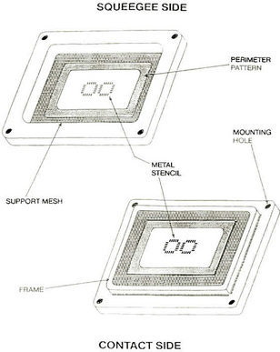
stencil A thick sheet material with a circuit pattern cut into the material. A metal mask is a stencil. The most common material is stainless steel.
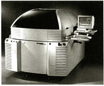
stencil printer Machine that dispenses solder paste or other material by means of a squeegee forcing material through the apertures of a stencil. Equipment ranges from manual to semiautomatic to automatic. (See Figure 13 on page 100.)
stencil wiper Peripheral device on some automatic stencil printers that automatically wipes the underside of the stencil between printing cycles. (See Figure 14.)
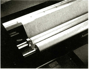
Figure 14 Stencil wiper as incorporated on automatic stencil printing machine. (Courtesy MPM Corporation)
step-and-repeat A process wherein the conductor or resistor patterns are repeated many times in evenly spaced rows onto a single film or substrate.
step-down stencil A stencil of varying thickness to accommodate coarse and fine-pitch deposits. Also known as multi-level stencil.
stonehenge effect A soldering defect in which a chip component has been pulled into a vertical or near vertical position with only one termination soldered to the PCB. It is typically caused by force imbalances during the reflow soldering process. Also referred to as drawbridging, tombstoning, and the Manhattan effect.
storage life The period of time during which a liquid resin or adhesive can be stored and remain suitable for use. Also called shelf life.
stress relief A method used to minimize stresses to the soldered termination or component usually in the form of a bend or service loop in a component lead and a solid or stranded wire to provide relief from stresses between terminations caused by movement, thermal expansion, or other external factor.
stripping Process of removal of resist.
subpanel A PCB panel containing multiple board images and used as the basic unit for assembly processing, as opposed to the full panel prepared for bare board fabrication. Hence, two or more subpanels result from the full panel.
substrate The base material that forms the support structure of an IC or PCB.
subtractive process A process for obtaining conductive patterns by the selective removal of unwanted portions of a conductive foil.
surface conditioners Specially formulated liquid cleaners to restore the solderability of the most commonly used metals and alloys in the soldering process.
surface insulation resistance The electrical resistance of the insulating material, determined under specified environmental and electrical conditions, between a pair of contacts, conductors, or grounding devices in various combinations, measured in ohms. Also referred to as SIR.
surface mount assembly (SMA) Electronics assembly in which non-through-hole components are mounted directly to the substrate surface.
surface mount component (SMC) A component designed to be mounted and soldered to pads on the surface of a PCB rather than inserted into through-holes in a PCB.
surface mount device Electronic components, either active (transistors, integrated circuits, diodes, etc.) or passive (capacitors, resistors, coils, etc.) that do not have wire leads or pins. The terminal leads are part of the component body, thus allowing direct mounting on the surface of printed circuit boards. Leaded devices are mounted by their leads through holes drilled in the boards. In both cases, the components are held in place on the boards, both mechanically and electrically, by solder. Surface mounted components usually are smaller than an equivalent through-hole leaded device and, in some cases, less expensive. Equipment and design engineers can save valuable wiring board area by mounting surface-mounted leadless components on the underside of a board, and conventional leaded components on the top side of boards. Abbreviated SMD.
surface mounting Electrical connection of components to the surface of a conductive pattern without using through-holes.
surface tension A property of liquids, due to molecular forces existing in the surface film of all liquids, which tends to contract the volume into a form with the least surface area. That is, the molecules on the surface of a liquid are not acted upon by the same forces as those molecules in the interior of the liquid.
surfactant A chemical added to water to lower the surface tension and to improve wetting. It is a short form for “surface active agent.”
suspension A mixture of liquid or solid in a liquid. It is not considered a true solution because discrete particles or droplets are visible and the mixture is not clear.
synthetic activated flux A high activity organic flux whose post soldering residues are soluble in commonly used halogenated solvents. Abbreviated SA.
syringe A tool that also packages a paste or epoxy in a container for manual, hydraulic, or pneumatic deposition through a needle opening.
syringe dispensing Material deposition by applying pressure (pneumatic or hydraulic) for a certain period of time to expel the appropriate amount of material through the needle to the target location.

Figure 15 Dispensing pump from automatic material dispensing machine used to dispense adhesives and solder paste. (Courtesy Camelot. Systems, Inc.)