Chapter 3
Measuring Memory
In the previous chapter, we explored measuring CPU performance, the first of the four fundamental hardware resources.
The second fundamental resource to measure is memory access latency—how long do real computer reads and writes take, for each level of the memory hierarchy? A simple measurement of the latency of a single data load is even more subtle than the measurement of arithmetic instructions. The goal in this chapter is to measure the size and organization of the typical four-level memory subsystem in modern machines.
3.1 Memory Timing
This is the most complex topic in Part I. We will examine several design layers, each with its own concepts and constraints. Because main memory is so much slower than CPUs, modern processors have many speedup mechanisms. Like the girl with a curl on her forehead, when they are good they are very, very good, and when they are bad they are horrid [Longfellow 1904]. Sometimes software will have memory access patterns that defeat the speedup mechanisms or cause them to do substantial unneeded work, producing bad performance. At the end of this chapter, you will have a much better understanding of today’s complex computer memory systems.
Many different design layers interact to produce memory access patterns and to deliver data with varying amounts of delay. These layers include
C programmer
Compiler
Assembly language
CPU instructions
Virtual memory
Several levels of cache memory
Main-memory DRAMs
Our two sample-server processors (Appendix A) have an Intel i3 chip and an AMD Ryzen chip, each with three levels of cache on chip and 8GB of dynamic random-access memory (DRAM) off chip in two dual-inline memory modules (DIMMs). Each i3 chip has two physical cores hyperthreaded to present the illusion of four cores. Each Ryzen processor chip has four physical cores. For both chips, each physical core has a dedicated L1 instruction cache and dedicated L1 data cache, plus a dedicated L2 combined cache. Each processor has a single L3 cache shared across all cores.
A datacenter server processor will have more complex chips with more cache and may have multiple processor chips per server. A desktop or embedded processor may have smaller and simpler caches. However, the measurements done here can also be performed on other processors. Along the way, you will learn more about memory hierarchies, and that in turn will inform your work on understanding software performance.
3.2 About Memory
As you recall from the previous chapter, in the 1950s golden age of computing simple instructions took two cycles to execute, one for instruction fetch and one for instruction execution that typically included a single memory access for data. This made sense when the CPU clock cycle time and core memory access times were identical.
At that time, main memories were constructed from ferrite cores (little 0.4mm iron-oxide donuts) with wires going through the holes (Figure 3.1), one core per bit of memory. Pulsing a positive current spike through a core magnetized it clockwise, and a negative spike magnetized it counterclockwise. The magnetization remained forever with no power supplied, providing a way to remember a single bit: 0 for one magnetic direction and 1 for the other.

Figure 3.1 Ferrite core memory [Wikimedia 2010]
Memories were arranged as words, not bytes (byte addressing arrived in 1964 [Amdahl 1964]). Depending on the computer, a word might be 36 bits or 48 or some other number. Core memories were physically arranged as a dense plane of wires and cores for a single bit of each memory word: all bit<0> cores for all memory words in one plane, all bit<1> cores in another plane, etc. A number of these planes were then stacked together to make a complete memory. For example, the IBM 7090 had 32K words of memory, each 36 bits. The 36 planes each contained 32,768 cores (there was no parity or error correction code, ECC).
Reading was done by pulsing a horizontal and a vertical wire in each plane to drive all the cores in a word to zero and then looking at the resulting electrical waveforms via the diagonal threaded sense wire to see if each addressed core switched magnetic state. If so, it had been a 1, and if not, it had been a 0. The readout was thus destructive. After reading, the bits read were then always restored—written back into the just-zeroed cores. Core memory cycle times for read + restore ran from 10 usec down to about 1 usec.
In 1964, John Schmidt at Fairchild Semiconductor invented the transistorized static random-access memory (SRAM) [ChipsEtc 2020a, Schmidt 1965, Schmidt 1964]. With six transistors per bit, SRAM is fast but somewhat expensive. With no magnetic state, the data in an SRAM disappears when power is removed.
The very first cache memory, in the 1968 IBM 360/85, was SRAM, called monolithic memory in the IBM papers [Liptay 1968] of the time.
Just two years after SRAM, Robert Dennard at IBM invented the dynamic random-access memory (DRAM) in 1966 [ChipsEtc 2020b, Wikipedia 2021m]. With just one transistor per bit, DRAM is much denser (and therefore cheaper) than SRAM, but slower to access.
In September 1970, the IBM System 370/145 was announced [IBM 1970]—the first commercial machine to switch to solid-state DRAM main memory, using IBM’s internally manufactured chips. The following month, Intel introduced the first commercially available dynamic random-access memory chip, the Intel 1103 DRAM (Figure 3.2), created by William Regitz and Joel Karp [Wikipedia 2020f]. By 1972 it was the best-selling semiconductor memory chip in the world—leading to the demise of core memory. (SRAM was too expensive to displace 1970s core memory.)

Figure 3.2 DRAM memory [Wikimedia 2016]
As in core memory, DRAM reading is destructive. Each read drains charge from the single storage transistor per bit, and the bits read are then written back to those transistors. Unlike SRAM memory, DRAM bits leak away after several milliseconds even with power supplied. DRAMs thus need to have every location refreshed—read and re-written—every 2 msec or so.
The performance of these various memory technologies interacts with programs’ access patterns to provide varying execution performance. This chapter covers measuring elements of a processor’s memory hierarchy, and the next chapter covers changing access patterns to take advantage of this hierarchy to speed up execution, or more often to avoid patterns that severely slow down execution.
3.3 Cache Organization
Today’s datacenter CPUs have a memory hierarchy consisting of several layers of cache memory plus a very large main memory, as shown in Figure 3.3. Each physical CPU core in a multicore processor chip has its own Level-1 instruction (L1i) and data (L1d) caches, each built out of very fast SRAM cells. These caches can usually access a new memory word or even two words every CPU cycle, with cycle times now around 0.3 nsec, about 250 times faster than the original 80 nsec cache in the IBM 360/85. Main memory cycle times have increased only by about a factor of 20 over the same time period.
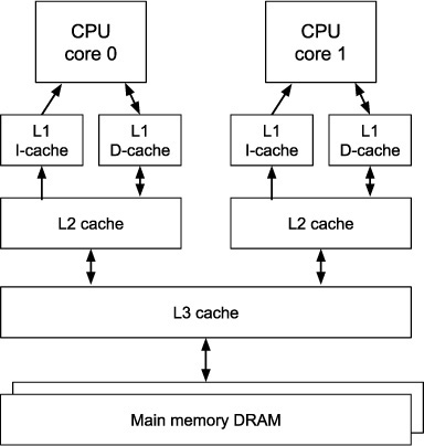
Figure 3.3 Typical multi-level cache memory organization for two CPU cores
Level-1 instruction and data caches typically are filled from a larger but slower combined Level-2 (L2) cache, sometimes one per physical CPU core, as in Figure 3.3, and sometimes shared across a few CPU cores. In turn, the Level-2 caches are filled from a larger and slower Level-3 (L3) cache that is on-chip and shared across all the cores. Some processors may even have a Level-4 cache.
A single large cache level would be best if it could be simultaneously fast enough, big enough, and shared enough. Unfortunately, that isn’t possible since semiconductor memory access times always get longer as the memory size gets bigger. Modern cache designs thus represent an engineering balance that delivers high performance with relatively low cost, so long as the memory-access patterns include a fair number of repeated accesses to the same locations. Over time, the details of this balance will change, but the general picture may not.
With L1 caches able to start one or two new low-latency accesses every CPU cycle and each bank of main memory systems unable to start a new access more often than about every 50–100 CPU cycles, the placement of data and instructions in the cache hierarchy has a huge effect on overall CPU performance. Some patterns are very, very good, while others are horrid.
Cache memory is organized as lines (or blocks) of several bytes each, with all the bytes of a line brought into or moved out of the cache together. Each cache line has an associated tag specifying the main memory address for its data (shown at the top of Figure 3.4). To find data in a cache, the cache hardware compares the memory address involved against one or more tags. If a match is found, termed a cache hit, the corresponding data is accessed quickly. If no match is found, termed a cache miss, the data must be accessed more slowly from a lower level of the memory hierarchy.
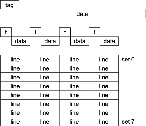
Figure 3.4 Cache organization: single cache line (top), a four-way associative cache set with four cache lines (middle), cache with eight sets, each four-way, tags not shown (bottom)
The minimum useful amount of data per cache line is two machine words, with a word most often the size of a pointer; this means for chips with 64-bit addresses, that two 8-byte pointers or 16 bytes total is the minimum practical cache line size. Smaller lines would spend too much hardware on tags and not enough on data. The maximum useful line size is one page in a virtual memory system, which means 4KB in most current chips. Thus, the only reasonable cache-line data sizes are
16, 32, 64, 128, 256, 512, 1024, 2048, and 4096 bytes
The most common choices in the industry are 64 and 128 bytes, but 32 and 256 bytes are sometimes seen. (The first cache in the IBM 360/85 had sixteen 1KB cache sectors and hence only 16 tags, but filled them in pieces by transferring 64-byte subblocks/sublines from main memory.)
In a fully associative cache, data at a given main memory address can be stored in any line in the cache. To find which one, the memory address is compared against all the tags in the cache. For a 32KB cache with 64B lines, this means comparing against all 512 tags at once—a lot of fast hardware. If one tag matches, then the corresponding line’s data are quickly accessed. If none matches, the data are accessed from a slower memory, typically also doing a fill—replacing some cache line so that a subsequent access to the same or nearby data will hit. (If more than one tag matches, there is a serious hardware bug.)
In contrast, a direct-mapped cache allows data at a given main memory address to be stored in exactly one possible cache line, usually chosen by low memory address bits to spread successive memory locations around the cache as much as possible. Direct-mapped caches perform poorly whenever two frequently accessed data items map to the same cache line: each access to one item removes the other one from the cache, so alternating accesses thrash the cache with 100% misses to slower memory.
A middle-ground design is the set-associative cache [Conti 1969]. Data at a given main memory address are stored in exactly one possible set of N cache lines for an N-way associative cache. Within each set, the memory address is compared against all the N tags. Typical values of N range from 2 to 16. In a four-way set-associative cache, each set contains four cache lines, as shown in the middle of Figure 3.4. Caches often have 2k sets so that the set selection can be done directly with low memory address bits; otherwise, some simple hash of the memory address is used to select the set. The bottom of Figure 3.4 shows a small four-way associative cache with eight sets total. For simplicity, the 32 tags are not shown. Three address bits are used to select the set, and then all four tags in that set are compared to the memory address being accessed. Note that sequential memory accesses would land within a cache line in some set and then move down, not sideways, in this picture to a line in the next set—for example, first accessing a line in set 0, then a line in set 1, etc. This design spreads sequential accesses across all sets. Common set-associative caches have 64 or more sets.
3.4 Data Alignment
In the following discussion, the term aligned is prominent. An aligned reference to a 4-byte item is at a byte address that is a multiple of 4. An aligned reference to an 8-byte item is at a byte address that is a multiple of 8, etc. Actual cache and memory accesses are done only in aligned quantities. Unaligned references are done by accessing two aligned locations and doing some byte shifting and merging to select the referenced bytes. When done in hardware, unaligned references are often a few cycles slower than aligned accesses. If done in a software unaligned-access-trap routine, unaligned references often take 100 cycles or more.
3.5 Translation Lookaside Buffer Organization
In addition to caches for instructions and data, modern processors provide virtual memory mapping and have translation lookaside buffers (TLBs) to hold frequently used virtual-to-physical mappings. In some cases, TLBs are constructed as a small Level-1 TLB per CPU core and a larger slower Level-2 TLB, either per core or shared across several cores. All this mechanism increases speed but also adds complexity and variability to CPU performance.
TLBs and cache designs interact. Most caches are physically addressed, meaning that set selection and tag values are from physical memory addresses, after translation from virtual addresses. The alternate design of virtually addressed cache is occasionally used, with set selection and tag values taken from the unmapped virtual address. This design has difficulties if two distinct virtual addresses map to the same physical address, since the different virtual addresses would map to different cache lines. Such duplicate mappings are not a problem if the data are read-only (such as instruction streams), but are an issue if data is written via one virtual address and then read via a different virtual address.
With a physically addressed cache bigger than one page, the virtual-to-physical mapping must be completed before cache tag comparisons can be started, and tag comparisons must be completed before cached data can be accessed by the CPU. These steps usually use the fastest possible hardware for L1 cache accesses, so can take noticeable amounts of power and chip area. To gain some speed, it is common to use unmapped lower-order virtual address bits to choose the right cache set before the virtual-to-physical mapping is completed. The number of unmapped low-order address bits thus determines the maximum size of a fast L1 cache—one of the under-appreciated costs of small pages.
Cache set choice based on unmapped address bits works only if the number of sets is small enough. For example, with a 4KB page, the low-order 12 address bits are unmapped. With a 64-byte cache line, the six lowest bits select a byte within a line, so at most the other six unmapped bits are available to select a cache set, so exactly 64 sets maximum. If the L1 cache is direct-mapped, it can be at most 64 sets of one line each, or 4KB total. If it is four-way associative, it can be at most 64 sets of four lines each or 16KB total. In general, overlapping the time for address mapping and tag access works only if the maximum L1 set-associative cache size is less than or equal to pagesize * associativity.
This unfortunate coupling means that small page sizes such as 4KB require small L1 caches. Eventually, the industry will need to move to larger page sizes, with more unmapped bits and hence an opportunity for modestly larger L1 caches. For a datacenter machine with 256GB of main-memory RAM, managing it as 4KB pages means there are 64 million pages of main memory, an excessively large number. It would be better and faster to have a somewhat larger page size and fewer total pages.
3.6 The Measurements
It is possible to look up in (often obscure) manufacturer literature such as a chip datasheet what the actual cache organization is for a given processor, but we want to find out via programs that can run on a wide variety of machines.
In this chapter we seek to measure the performance of each layer of the memory hierarchy and in the process gain some insight to the dynamics of single and multiple instruction threads as they compete for shared memory resources. Our objective is for you to learn techniques to tease out memory performance characteristics so that you can better understand and estimate program performance and better understand what is happening when access patterns defeat the speedup normally provided by a cache hierarchy.
Our measurement will be done in three steps, the first two of which are done in the supplied mystery2.cc program:
Determine the cache line size.
Determine the total size of each level of cache.
Determine the associativity of each layer of cache.
As with measuring instruction latency in the previous chapter, the straightforward approach to measuring memory parameters is to do something like
Read time.
Access memory in some pattern.
Read time.
Subtract.
However, this is tricky in a modern execution environment. We will explore each step in a little more detail.
For concreteness, the details in the following discussion are based on a sample server (Appendix A) with a representative processor, the Intel i3. Other processors have similar memory hierarchies but the speeds, sizes, and organization may differ.
3.7 Measuring Cache Line Size
How can we have a program discover the cache line size? There are several design choices and several available dead-ends. One choice is to start with a cache containing none of the data we are about to access, load an aligned word at location X, and then load the word at X + c, where c is a possible cache line size.
If X is aligned on a cache line boundary and c is less than the line size, loading X + c will hit in the cache because it was brought in as part of a single cache line when X was brought in. Figure 3.5 shows twelve sequential accesses and where they land in the four-way eight-set cache of Figure 3.4. In Figure 3.5a, c is 1/4 of the line size, so the first four accesses are in the same line, the next four in the next line, etc. The twelve accesses thus cover three cache lines and therefore encounter just three misses. In Figure 3.5b, c is 1/2 of the line size, so pairs of accesses are in the same line, encountering six cache misses total for our twelve accesses. In Figures 3.5c and 3.5d, all twelve accesses miss.
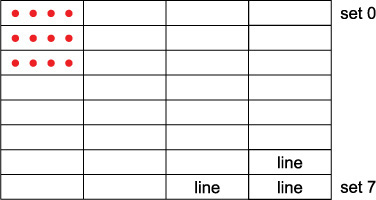
Figure 3.5a Accesses spaced 1/4 of a cache line apart and therefore landing in three lines in three successive sets

Figure 3.5b Spaced 1/2 a cache line apart, landing in six lines in three sets
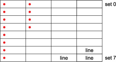
Figure 3.5c Spaced one cache line apart, landing in twelve lines across the eight sets but with multiple lines in some sets

Figure 3.5d Spaced two cache lines apart, landing in twelve lines across just four sets, three lines per set of the four-way associative choices
If X is aligned on a cache line boundary and c is greater than or equal to the line size, then loading X + c will not hit in the cache. Assuming that cache misses are on the order of 10 times slower than cache hits, we can time a loop doing a few hundred loads to different possible increments (strides) and distinguish those values of c that are fast and those that are slow. The smallest slow c is the cache line size.
What would we expect to see? It is an important professional design discipline to ask this question at this point in your thought process and to write down or sketch for yourself what you expect. Only then can you react quickly to finding something quite different. Assume for a moment that the real cache line size is 128 bytes. For accesses to an array of items spaced 16 bytes apart (a stride of 16), the first eight items all fit into one cache line, the second eight into another, etc. If we fetched 200 consecutive items, we would expect to see 200/8 = 25 cache misses. If instead we access stride-32 items, we would expect to see 200/4 = 50 cache misses. For stride-128 items and greater, we would expect to see 200 cache misses every time. If we sketch a graph of the time per access (load), we might expect something like Figure 3.6, where the average time per load starts out as 1/8 the real miss time, then 1/4, then 1/2, then all the rest are the real miss time, 100% misses.
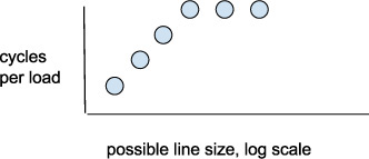
Figure 3.6 Sketch of expected access times vs. stride
3.8 Problem: N+1 Prefetching
This sequential-stride design choice of using addresses X, X + c, X + 2c, ... sounds good but turns out to be too simplistic. Modern caches often prefetch line N + 1 when line N is accessed, removing all but the first cache miss in our access pattern. Also, modern CPUs do out-of-order execution, launch multiple instructions per CPU cycle, and may well have 5–50 outstanding loads waiting in parallel for memory responses. The effect can be to make many cache misses take about the same time as just one miss, reducing the apparent miss time by over a factor of 10.
The supplied program mystery2.cc implements this choice of sequential-stride accesses in the routine NaiveTiming(), so you can see that it gives uniformly misleading results that are too fast. The inner loop accesses 16-byte items spaced pairstride apart. The caller varies the stride, clearing the cache between calls by loading 40MB of unrelated data. I picked 40MB because it is somewhat larger than the largest expected cache size of 32MB. This number may have to be increased for future chips with larger caches. Nothing here attempts to defeat prefetching or parallel misses. See Code Sample 3.1.
Code Sample 3.1 Naive load loop
  // We will read and write these 16-byte pairs, allocated at different strides
  struct Pair {
   Pair* next;
   int64 data;
  };

  int64 NaiveTiming(uint8* ptr, int bytesize, int bytestride) {
    const Pair* pairptr = reinterpret_cast<Pair*>(ptr);
    int pairstride = bytestride / sizeof(Pair);
    int64 sum = 0;

    // Try to force the data we will access out of the caches
    TrashTheCaches(ptr, bytesize);

    // Load 256 items spaced by stride
    // May have multiple loads outstanding; may have prefetching
    // Unroll 4 times to attempt to reduce loop overhead in timing
    uint64 startcy = __rdtsc();
    for (int i = 0; i < 256; i += 4) {
      sum += pairptr[0 * pairstride].data;
      sum += pairptr[1 * pairstride].data;
      sum += pairptr[2 * pairstride].data;
      sum += pairptr[3 * pairstride].data;
      pairptr += 4 * pairstride;
  }
  uint64 stopcy = __rdtsc();
  int64 elapsed = stopcy - startcy;    // Cycles

  // Make sum live so compiler doesn't delete the loop
  if (nevertrue) {

      fprintf(stdout, "sum = %ld
", sum);
    }
    return (elapsed >> 8);            // Cycles per one load
  }
3.9 Dependent Loads
Another design choice is to build a linked list of items in memory, with each item the size of a possible cache line and aligned on a cache line boundary. Each item contains a pointer to the next sequential item, as shown in Figure 3.7a. Then if ptr points to the first item, a loop of ptr = ptr->next will do a series of loads, but the address for each load depends on the value fetched by the previous load, so they must be executed strictly sequentially, defeating out-of-order execution, multiple instructions per CPU cycle, and multiple parallel outstanding loads. This design also allows us to see how long the load-to-use latency is for each level of the memory subsystem.
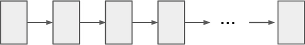
Figure 3.7a Linear list of items
The supplied program mystery2.cc implements this choice in the routine LinearTiming(), so you can see that it gives better but also misleading results. One remaining problem is that the linked lists do not defeat cache prefetching.
To attempt to defeat prefetching, we can build the linked lists so that the items are scrambled around in the address space, as shown in Figure 3.7b.
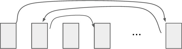
Figure 3.7b Scrambled list of items
This helps but is not sufficient. When the leftmost scrambled item is in fact the line size, fetching it may still cause the hardware to prefetch the next-to-leftmost item. Even though this item is not accessed immediately, it will be accessed later and can therefore be a hit when we are hoping the design produces a miss.
3.10 Non-random Dynamic Random-Access Memory
It turns out there is another complication. We count cache misses by timing a few hundred memory loads and expect twice as many misses to take about twice as long. But when you look at main memory DRAM designs, you find a surprise. Access times are not random (in spite of “random” in the name). Actual DRAM chips first access a row of a big array of bits inside the chip and then access a column of bytes from that row. A so-called precharge cycle precedes the row access, to set the internal data lines to about half the power-supply voltage, so that reading only a little charge in a bit cell is enough to get the data lines off dead center quickly. Sense amplifiers within the chip quickly drive these small read changes to full zero or one voltage levels. Each of the precharge, row access, and column access cycles takes about 15 nsec.
Rows are typically 1,024 bytes, and a dual inline memory module (DIMM, memory card) typically has eight DRAM chips cycled in parallel to produce eight bytes at once, driving an 8-byte-wide memory bus to the CPU chip. In this case, the effective row size across the eight DRAM chips is 8 *1,024 = 8,192 bytes. A CPU with two memory buses connected to two DIMMs usually stores successive cache lines in alternating DIMMs to achieve a 2x bandwidth improvement when accessing multiple sequential cache lines. In this case, the effective row size is 2 * 8KB = 16KB. Our sample server has this organization.
If two successive accesses to a DRAM are in two different rows, the sequence
precharge, row access, column access
occurs for each. But if the second access is to the same row as the first one, the CPU and DRAM hardware implement a shortcut; just the
column access
occurs for the second one. This is approximately three times faster than the full sequence. A 3x variation in memory access time is a large amount of distortion if we are trying to measure a 2x difference in total time. So we may also have to defeat the DRAM shortcut timing.
We do this when building the linked lists by flipping the 16KB address bit in every other list item, explicitly putting successive items into different DRAM rows. In the supplied mystery2.cc program, routine MakeLongList(), this is the purpose of the variable extrabit.
The supplied program mystery2.cc implements all this in the routine ScrambledTiming(), so you can see that it gives better results that finally look a bit like our earlier sketch. There are a few more details to consider in the exercises at the end of this chapter.
In Figure 3.8 we see one set of results. Your results will differ somewhat. The scrambled cycles per load shows the expected approximate doubling per 2x stride change, flattening off at about 200 cycles for stride 128 bytes and above. The actual line size is 64 bytes, but even our scrambled measurement did not completely defeat the cache prefetcher(s) and same-row DRAM access optimization. The linear measurement is distorted by prefetching all the way out to 512 byte stride, while the naive measurement is not measuring load latency at all. The extra cycles at stride 4,096 bytes most likely reflect 100% TLB misses.
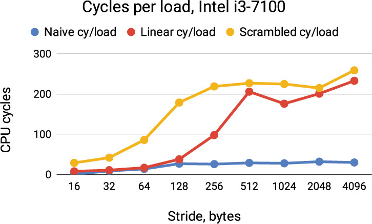
Figure 3.8 Cycles per load for different strides and different measurement techniques. Compare to the sketch in Figure 3.6.
Virtual-to-physical address mapping means that all the pictures in our heads about cache layout are too simplistic. The physical addresses that the caches see match our pictures only for the low-order 12 address bits—all the higher physical address bits are unpredictable, adding noise to most of our measurements and making timing changes less sharp.
3.11 Measuring Total Size of Each Cache Level
Once we have the cache line size, we next want to know for each level of the cache hierarchy how big it is. The total size of the L1 cache informs data structure designs that have working sets that likely fit into the L1 cache and hence are faster than designs that don’t fit. The same consideration applies to L2 and L3.
Our strategy for finding the size of each cache level is to read N bytes into the cache and then reread, looking at timings. If all N bytes fit in the cache, then the rereads will be fast. If the bytes don’t fit, then some or all of the rereads will miss and be filled from the next level down, assuming (as is always the case) that each level is bigger than the previous one. In contrast to the previous section, where we were either hitting in the L1 cache or going to main memory that is O(100) times slower, our measurements in this section will be comparing L1 hits to L2 hits, or L2 hits to L3 hits, etc., where each level is only O(5) times slower than the previous one.
Timings on real machines and operating systems are rarely exactly repeatable. External interrupts, network traffic, humans typing, and background programs such as browsers or display software all contribute to small time variations in multiple runs of the same program. Our timing data will thus always be a bit noisy. The relatively small difference in adjacent memory-level times will make timings somewhat harder to evaluate.
What would we expect to see? For N <= L1 cache total size, we would expect the re-reads to be fast at just a few cycles per load, the L1 access time. For L1size < N <= L2size, we would expect to see mostly the somewhat slower L2 access time, etc. The result may look like the Figure 3.9 sketch, with L1 cache hits in the bottom row, L2 in the middle row, L3 in the top row, and main memory not shown but above the top row.
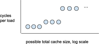
Figure 3.9 Sketch of expected access times vs. number of bytes accessed
Since there will be some noise in this measurement, it is helpful to run each experiment several times. The supplied mystery2.cc routine FindCacheSizes() does each timing measurement in four passes, using simple linear stride. The first time initializes the cache by loading from main memory so is always slow and is to be ignored here. The next three times should all be similar and show the time difference we seek. The program results are given in count of cache lines, not kilobytes. I multiplied by an assumed or previously measured 64B per cache line to get the graph in Figure 3.10, which shows one set of measured results.

Figure 3.10 Cycles per load for different total sizes touched. Compare to Figure 3.9.
Loading 1KB of data into the cache and then re-reading it is fast, at about four cycles per load. The same is roughly true for 2–16KB. At 32KB, things slow down a little to about eight cycles per load. For 64–256KB, loads take about 14 cycles each. For 512–2048KB, loads take 20–24 cycles each. Above 2048KB (2MB) the load time quickly rises to 70–80 cycles each. The actual L1 cache on this chip is 32KB and has a three- or four-cycle load-use latency. The L2 cache is 256KB and about 14 cycles, and the L3 cache is 3MB and roughly 40 cycles. The 3MB size falls between the 2MB and 4MB measurements we made in Figure 3.10.
The timing of about eight cycles per load for 32KB of data should be closer to four cycles in a fully used 32KB cache. Why? We implicitly assumed that accessing 32KB of data would exactly fill the 32KB L1 data cache. This assumption depends on there being nothing else accessed in the L1 cache and depends on the allocation policy being true least recently used (LRU), or true round-robin. In reality, the mystery2.cc program itself has a few variables that use the L1 cache, and the cache replacement policy is not perfect LRU, leading to some underutilization of the cache and thus some misses out to the L2 cache. Both of these make the measurement somewhat slower when our total data is just under the total cache size.
A different phenomenon occurs at 64KB and 512KB, just above the size of the L1 and L2 caches, respectively. In a not-perfect-LRU environment, some of the 64KB of data expected to be found in L2 is instead found in the L1 cache because it happened not to be replaced. This gives a slightly fast overall average load time at 64KB, and similarly for some of the 512KB of data found in the L2 cache instead of L3. As you should expect by now, our measurement and hence our graph do not have the sharp step-function boundaries we had in the Figure 3.9 sketch.
3.12 Measuring Cache Associativity of Each Level
Once we have the line size and the total size of each cache level, we can find the associativity of each cache. In a fully associative cache, a given cache line can go any place at all in the cache. In a set-associative cache, a given cache line can go in a small number of places, within just one set. If a given cache line can go only one place in the cache, the set size is 1, and the cache is direct mapped or one-way associative. If a cache line can go two places in the cache, it is two-way associative, etc.
An N-way associative cache usually accesses all N possible tags and data locations in parallel (using almost N times as much electrical power as accessing one location). If one of the tags matches the given address, there is a cache hit, and the corresponding data is used. If none matches, there is a cache miss at that level.
Our strategy for finding the cache associativity at each cache level is to read a list consisting of addresses in A distinct lines with those addresses repeated many times, e.g. for A=4,
0 4K 8K 12K 0 4K 8K 12K 0 4K 8K ...
The addresses are picked so they all go into just set[0] of the cache. Then re-read the list, looking at timings. If all A distinct lines fit into set[0], then the re-reads will be fast. If they don’t fit, then the re-reads will miss and be filled from the next level down. The largest number A that fit at once is the cache associativity. The supplied mystery2.cc program does not measure cache associativity. In the exercises, you get to do this one.
If the L2, etc., caches have higher associativity than the L1 cache, you should be able to find the L2, etc., values. But if they have less associativity than the L1 cache, hits in L1 may obscure the timing you would like to see for the other cache levels. In that case, you could look for an address pattern that spreads across a small number of associative sets in the L2 cache but all land in a single set in the L1 cache, overwhelming the L1 associativity and forcing misses out to L2.
3.13 Translation Buffer Time
We aren’t quite done with complications. While accessing memory in today’s processors, we are also accessing the virtual-memory page tables. Reading tens of megabytes of data to trash the caches also trashes the hardware TLB in a CPU core. Some subsequent memory accesses must first do a page-table memory access to load the corresponding TLB entry, at least doubling the total access time for those.
If there are 16-byte items being accessed, i.e., stride 16, then 256 of these fit in a single 4KB page, so accessing all 256 involves just one TLB miss. But if there are 4KB items being accessed, stride 4KB, loading from 256 of these will get 256 TLB misses, not just one. The TLB miss times thus may distort all our earlier measurements, but in a predictable way.
3.14 Cache Underutilization
The final complication we discuss is that of cache underutilization. Normally, the lowest bits of a memory address are used to pick which bytes to use in a cache line. If the line size is 64 bytes, this would be the lowest 6 bits. The next higher bits are used to select the associative set. If a tiny cache is 2KB organized as 64-byte lines, there are 32 cache lines total. If these are organized four-way associative, then there are eight sets of four cache lines each, as in Figures 3.4 and 3.5. With the low six address bits selecting a byte within a line, the next higher three address bits would be used to select the set, and the remaining higher bits would be compared against four tags in that set to determine a hit.
If we load data into a cache with 64-byte lines, but only load data spaced at multiples of 128 bytes, one of the address bits used to select a set will always be 0. So set[0], set[2], set[4], etc., will be used, but the other 1/2 of the sets will not be used. This means that the effective cache size is not 2KB but only 1KB. This is something to keep in mind when accessing regular address patterns. Figure 3.5d shows this effect, with the odd-numbered sets not used and shown in gray. We will see more of this effect in the next chapter when accessing columns of an array. For now, just keep in mind that underutilized cache equals slower execution.
3.15 Summary
In this chapter we examined and measured memory hierarchies consisting of multiple levels of cache plus DRAM main memory. Hierarchies are needed to strike an engineering balance between fast access at nearly CPU speed and the much slower access time inherent in very large DRAM memories. We explored some of the many speedup mechanisms used in modern CPUs while accessing memory and then defeated some of these to try to get meaningful measurements of just the memory access times for various patterns. Carefully chosen patterns inform us of the memory system organization. They also inform us about access patterns that will create performance problems.
Estimate what you expect to see.
Page size limits physically addressed L1 cache size.
Stride patterns reveal cache organization.
Total-size patterns reveal cache sizes.
Prefetching, multi-issue, out-of-order execution, and non-dependent loads make careful memory measurements difficult.
Virtual-address mapping makes patterns inexact.
TLB misses distort cache timings.
Patterns that produce cache underutilization can produce performance problems.
Compare your measurements against expectations. There is always learning in the discrepancies.
Exercises
Starting with the supplied mystery2.cc program compiled optimized, –O2, answer some questions, do some modifications, and then answer some more questions. You shouldn’t need to spend more than about two hours on the initial questions 3.1 through 3.7, plus maybe two more on question 3.8. If you are spending much more time, set it aside and do something else, or chat with a friend about the problem.
You will find it helpful to use a spreadsheet such as Microsoft Excel or Google Charts to turn the numbers into graphs so you can compare them to your sketches and think about what the patterns are telling you. Always label the x- and y-axis of your graphs, giving the units: counts, cycles, msec, KB, etc. Do this even if you are the only one looking at the graph. At some point, it will save you from making an order-of-magnitude error or from coming to a completely false conclusion. Once you develop this habit, it will save time.
Before you change things, rerun mystery2.cc a few times to see what the inherent variation is like in the cycle counts.
3.1 In the first part of mystery2.cc that looks at cache line size timings, what do you think the cache line size is, and why? If you have access to sample servers with more than one type of CPU chip, be sure to specify which server you measured.
3.2 In the first part of mystery2.cc that looks at cache line size timings, explain a little about the three timings for a possible line size of 256 bytes. These are the ones that should be about 30, 80, and 200 cycles per load.
3.3 In the first part of mystery2.cc that looks at cache line size timings, make a copy of the program, and in routine MakeLongList(), add a line after
int extrabit = makelinear ? 0 : (1 << 14);
that defeats the DRAM different-row address patterns:
extrabit = 0;
Explain a little about the changes this produces in the scrambled timings, especially for possible line size of 128 bytes. Keep in mind that the virtual-to-physical address mapping will somewhat corrupt the alternate different-row pattern before your change and will somewhat corrupt the same-row pattern afterward.
3.4 In the second part that looks at total cache size FindCacheSizes(), what do you think are the total sizes of the L1, L2, and L3 caches?
3.5 What is your best estimate of the load-to-use time in cycles for each cache level?
3.6 To run on a CPU with a non-power-of-2 cache size, such as an Intel i3 with 3MB L3 cache, how would you modify the program slightly to test for somewhat-common not-power-of-2 sizes? (You need not do the modification; just explain what you would do.)
3.7 In the second part that looks at total cache size FindCacheSizes(), explain a bit about the variation in cycle counts within each cache level. The ones that barely fill a level are somewhat faster than the ones that completely fill a level. Why could that be?
3.8 Implement FindCacheAssociativity(). What is the associativity of each cache level?