
10
INSTRUCTION SET ARCHITECTURE

This chapter discusses the implementation of a CPU’s instruction set. Although the choice of a given instruction set is usually beyond a software engineer’s control, understanding the decisions a hardware design engineer has to make when designing a CPU’s instruction set can definitely help you write better code.
CPU instruction sets contain several tradeoffs based on assumptions that computer architects make about the way software engineers write code. If the machine instructions you choose match those assumptions, your code will probably run faster and require fewer machine resources. Conversely, if your code violates the assumptions, chances are pretty good it won’t perform as well as it otherwise could.
Although studying the instruction set may seem like a task suited only to assembly language programmers, even high-level language programmers can benefit from doing so. After all, every HLL statement maps to some sequence of machine instructions, and the general concepts of instruction set design are portable across architectures. Even if you never intend to write software using assembly language, it’s important to understand how the underlying machine instructions work and how they were designed.
10.1 The Importance of Instruction Set Design
While features like caches, pipelining, and superscalar implementation can all be grafted onto a CPU long after the original design is obsolete, it’s very difficult to change the instruction set once a CPU is in production and people are writing software using it. Therefore, instruction set design requires very careful consideration; the designer must get the instruction set architecture (ISA) correct from the start of the design cycle.
You might assume that the “kitchen sink” approach to instruction set design—in which you include every instruction you can dream up—is best. However, instruction set design is the epitome of compromise management. Why can’t we have it all? Well, in the real world there are some nasty realities that prevent this:
Silicon real estate The first nasty reality is that each feature requires some number of transistors on the CPU’s silicon die (chip), so CPU designers have a “silicon budget”—a finite number of transistors to work with. There simply aren’t enough transistors to support putting every possible feature on a CPU. The original 8086 processor, for example, had a silicon budget of fewer than 30,000 transistors. The 1999 Pentium III processor had a budget of over 9 million transistors. The 2019 AWS Graviton2 (ARM) CPU has over 30 billion transistors.1 These three budgets reflect the differences in semiconductor technology from 1978 to today.
Cost Although it’s possible to use billions of transistors on a CPU today, the more transistors used, the more expensive the CPU. For example, at the beginning of 2018, Intel i7 processors using billions of transistors cost hundreds of dollars, whereas contemporary CPUs with 30,000 transistors cost less than a dollar.
Expandability It’s very difficult to anticipate all the features people will want. For example, Intel’s MMX and SIMD instruction enhancements were added to make multimedia programming more practical on the Pentium processor. Back in 1978, when Intel created the first 8086 processor, very few people could have predicted the need for these instructions. A CPU designer must allow for making extensions to the instruction set in future members of the CPU family to accommodate currently unanticipated needs.
Legacy support for old instructions This nasty reality is almost the opposite of expandability. Often, an instruction that the CPU designer feels is important now turns out to be less useful than expected. For example, the loop and enter instructions on the 80x86 CPU see very little use in modern high-performance programs. It’s commonly the case that programs never use some of the instructions in a CPU adopting the kitchen sink approach. Unfortunately, once an instruction is added to the instruction set, it has to be supported in all future versions of the processor, unless few enough programs use the instruction that CPU designers are willing to let those programs break.
Complexity A CPU designer must consider the assembly programmers and compiler writers who will be using the chip. A CPU employing the kitchen sink approach might appeal to someone who’s already familiar with that CPU, but no one else will want to learn an overly complex system.
These problems with the kitchen sink approach all have a common solution: design a simple instruction set for the first version of the CPU, and leave room for later expansion. This is one of the main reasons the 80x86 has proven to be so popular and long-lived. Intel started with a relatively simple CPU and figured out how to extend the instruction set over the years to accommodate new features.
10.2 Basic Instruction Design Goals
The efficiency of your programs largely depends upon the instructions that they use. Short instructions use very little memory and often execute rapidly, but they can’t tackle big tasks. Larger instructions can handle more complex tasks, with a single instruction often doing the work of several short instructions, but they may consume excessive memory or require many machine cycles to execute. To enable software engineers to write the best possible code, computer architects must strike a balance between the two.
In a typical CPU, the computer encodes instructions as numeric values (operation codes, or opcodes) and stores them in memory. Encoding these instructions is one of the major tasks in instruction set design, requiring careful thought. Instructions must each have a unique opcode, so the CPU can differentiate them. With an n-bit number, there are 2n different possible opcodes, so to encode m instructions requires at least log2(m) bits. The main point to keep in mind is that the size of individual CPU instructions is dependent on the total number of instructions that the CPU supports.
Encoding opcodes is a little more involved than assigning a unique numeric value to each instruction. As the previous chapter discussed, decoding each instruction and executing the specified task requires actual circuitry. With a 7-bit opcode, we could encode 128 different instructions. To decode each of these 128 instructions requires a 7- to 128-line decoder—an expensive piece of circuitry. However, assuming that the instruction opcodes contain certain (binary) patterns, a single large decoder can often be replaced by several smaller, less expensive ones.
If an instruction set contains 128 unrelated instructions, there’s little you can do other than decode the entire bit string for each instruction. However, in most architectures the instructions fall into categories. On the 80x86 CPUs, for example, mov(eax, ebx); and mov(ecx, edx); have different opcodes, because they’re different instructions, but they’re obviously related in that they both move data from one register to another. The only difference is their source and destination operands. Thus, CPU designers could encode instructions like mov with a subopcode, and then they could encode the instruction’s operands using other bit fields within the opcode.
For example, given an instruction set with only eight instructions, each with two operands, and each operand having only one of four possible values, we could encode the instructions using three packed fields containing 3, 2, and 2 bits, respectively (see Figure 10-1).
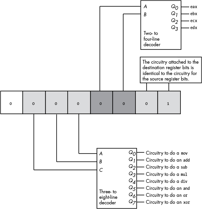
Figure 10-1: Separating an opcode into several fields to simplify decoding
This encoding needs only three simple decoders to determine what the CPU should do. While this is a basic example, it demonstrates one very important facet of instruction set design: opcodes should be easy to decode. The easiest way to simplify the opcode is to construct it using several different bit fields. The smaller these bit fields are, the easier it will be for the hardware to decode and execute the instruction.
The CPU designer’s goal, then, is to assign an appropriate number of bits to the opcode’s instruction field and to its operand fields. Choosing more bits for the instruction field lets the opcode encode more instructions, just as choosing more bits for the operand fields lets the opcode specify a larger number of operands (often memory locations or registers). You might think that when encoding 2n different instructions using n bits, you’d have very little leeway in choosing the size of the instruction. It’s going to take n bits to encode those 2n instructions; you can’t do it with any fewer. It is possible, however, to use more than n bits. This might seem wasteful, but sometimes it’s advantageous. Again, picking an appropriate instruction size is one of the more important aspects of instruction set design.
10.2.1 Choosing Opcode Length
Opcode length isn’t arbitrary. Assuming that a CPU is capable of reading bytes from memory, the opcode will probably have to be some multiple of 8 bits long. If the CPU is not capable of reading bytes from memory (most RISC CPUs read memory only in 32- or 64-bit chunks), the opcode will be the same size as the smallest object the CPU can read from memory at one time. Any attempt to shrink the opcode size below this limit is futile. In this chapter, we’ll work with the first case: opcodes that must have a length that is a multiple of 8 bits.
Another point to consider is the size of an instruction’s operands. Some CPU designers include all operands in their opcode. Other CPU designers don’t count operands like immediate constants or address displacements as part of the opcode, and this is the approach we’ll take.
An 8-bit opcode can encode only 256 different instructions. Even if we don’t count instruction operands as part of the opcode, having only 256 different instructions is a stringent limit. Though CPUs with 8-bit opcodes exist, modern processors tend to have far more than 256 different instructions. Because opcodes must have a length that is a multiple of 8 bits, the next smallest possible opcode size is 16 bits. A 2-byte opcode can encode up to 65,536 different instructions, though the instructions will be larger.
When reducing instruction size is an important design goal, CPU designers often employ data compression theory. The first step is to analyze programs written for a typical CPU and count how many times each instruction occurs over a large number of applications. The second step is to create a list of these instructions, sorted by their frequency of use. Next, the designer assigns the 1-byte opcodes to the most frequently used instructions; 2-byte opcodes to the next most frequently used instructions; and opcodes of 3 or more bytes to the rarely used instructions. Although this scheme requires opcodes with a maximum size of 3 or more bytes, most of the actual instructions in a program will use 1- or 2-byte opcodes. The average opcode length will be somewhere between 1 and 2 bytes (let’s say 1.5 bytes), and a typical program will be shorter than had all the instructions employed a 2-byte opcode (see Figure 10-2).
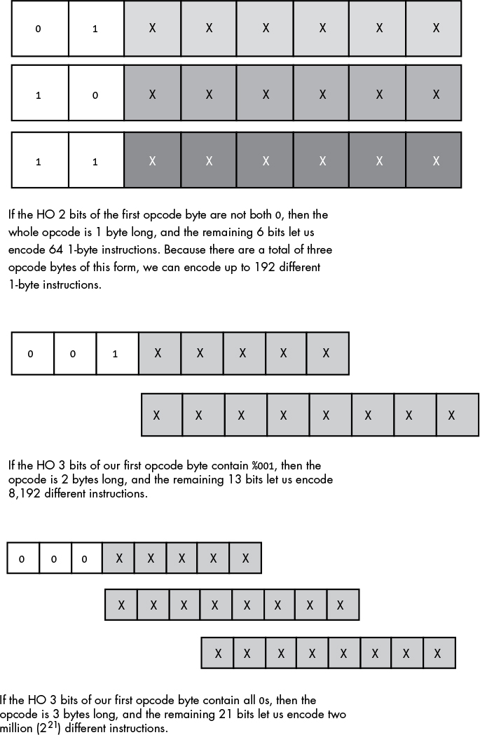
Figure 10-2: Encoding instructions using a variable-length opcode
Although using variable-length instructions allows us to create smaller programs, it comes at a price. First, decoding variable-length instructions is a bit more complicated than decoding fixed-length instructions. Before decoding a particular instruction field, the CPU must first decode the instruction’s size, which consumes time. This may affect the CPU’s overall performance by introducing delays in the decoding step, which in turn limits the CPU’s maximum clock speed (because those delays stretch out a single clock period, thus reducing the CPU’s clock frequency). Variable-length instructions also make decoding multiple instructions in a pipeline difficult, because the CPU can’t easily determine the instruction boundaries in the prefetch queue.
For these reasons and others, most popular RISC architectures avoid variable-length instructions. However, in this chapter, we’ll study a variable-length approach, because saving memory is an admirable goal.
10.2.2 Planning for the Future
Before actually choosing the instructions to implement in a CPU, designers must plan for the future. As explained earlier, the need for new instructions will undoubtedly arise after the initial design, so it’s wise to reserve some opcodes specifically for expansion purposes. Given the instruction opcode format in Figure 10-2, it might not be a bad idea to reserve one block of 64 1-byte opcodes, half (4,096) of the 2-byte opcodes, and half (1,048,576) of the 3-byte opcodes for future use. Giving up 64 of the very valuable 1-byte opcodes may seem extravagant, but history suggests that such foresight is rewarded.
10.2.3 Choosing Instructions
The next step is to choose the instructions to implement. Even if nearly half the instructions have been reserved for future expansion, that doesn’t mean that all the remaining opcodes must be used to implement instructions. A designer can leave a number of these instructions unimplemented, effectively reserving them for the future as well. The right approach is not to use up the opcodes as quickly as possible, but rather to produce a consistent and complete instruction set given the design compromises. It’s much easier to add an instruction later than it is to remove one, so, for the first go-round, it’s generally better to go with a simpler design.
First, choose some generic instruction types. Early in the design process it’s important to limit your choices to very common instructions. Other processors’ instruction sets are probably the best place to look for suggestions. For example, most processors have the following:
- Data movement instructions (such as mov)
- Arithmetic and logical instructions (such as add, sub, and, or, not)
- Comparison instructions
- Conditional jump instructions (generally used after the comparison instructions)
- Input/output instructions
- Other miscellaneous instructions
The initial instruction set should comprise a reasonable number of instructions that will allow programmers to write efficient programs, without exceeding the silicon budget or violating other design constraints. This requires CPU designers to make strategic decisions based on careful research, experimentation, and simulation.
10.2.4 Assigning Opcodes to Instructions
After choosing the initial instructions, the CPU designer assigns opcodes to them. The first step in this process is to group the instructions according to the characteristics they share. For example, an add instruction probably supports the exact same set of operands as the sub instruction, so it makes sense to group these two instructions together. On the other hand, the not and neg instructions each generally require only a single operand. Therefore, it makes sense to put these two instructions in the same group, but one separate from the add and sub group.
Once all the instructions are grouped, the next step is to encode them. A typical encoding scheme uses some bits to select the group, some to select a particular instruction from that group, and some to encode the operand types (such as registers, memory locations, and constants). The number of bits needed to encode all this information can have a direct impact on the instruction’s size, regardless of how often the instruction is used. For example, suppose 2 bits are needed to select an instruction’s group, 4 bits to select the instruction within that group, and 6 bits to specify the instruction’s operand types. In this case, the instructions are not going to fit into an 8-bit opcode. On the other hand, if all we need is to push one of eight different registers onto the stack, 4 bits will be enough to specify the push instruction group, and 3 bits will be enough to specify the register.
Encoding instruction operands with a minimal amount of space is always a problem, because many instructions allow a large number of operands. For example, the generic 32-bit 80x86 mov instruction allows two operands and requires a 2-byte opcode.2 However, Intel noticed that mov(disp, eax); and mov(eax, disp); occur frequently in programs, so it created a special 1-byte version of these instructions to reduce their size and, consequently, the size of programs that use them. Intel did not remove the 2-byte versions of these instructions, though: there are two different instructions that store EAX into memory and two different instructions that load EAX from memory. A compiler or assembler will always emit the shorter versions of each pair of instructions.
Intel made an important tradeoff with the mov instruction: it gave up an extra opcode in order to provide a shorter version of one variant of each instruction. Actually, Intel uses this trick all over the place to create shorter and easier-to-decode instructions. Back in 1978, creating redundant instructions to reduce program size was a good compromise given the cost of memory. Today, however, a CPU designer would probably use those redundant opcodes for different purposes.
10.3 The Y86 Hypothetical Processor
Because of enhancements made to the 80x86 processor family over time, Intel’s design goals in 1978, and the evolution of computer architecture, the encoding of 80x86 instructions is very complex and somewhat illogical. In short, the 80x86 is not a good introductory example of instruction set design. To work around this, we’ll discuss instruction set design in two stages: first, we’ll develop a trivial instruction set for the Y86, a hypothetical processor that is a small subset of the 80x86, and then we’ll expand our discussion to the full 80x86 instruction set.
10.3.1 Y86 Limitations
The hypothetical Y86 processor is a very stripped-down version of the 80x86 CPUs. It supports only:
- One operand size: 16 bits. This simplification frees us from having to encode the operand size as part of the opcode (thereby reducing the total number of opcodes we’ll need).
- Four 16-bit registers: AX, BX, CX, and DX. This lets us encode register operands with only 2 bits (versus the 3 bits the 80x86 family requires to encode eight registers).
- A 16-bit address bus with a maximum of 65,536 bytes of addressable memory.
These simplifications, plus a very limited instruction set, will allow us to encode all Y86 instructions using a 1-byte opcode and a 2-byte displacement/offset when applicable.
10.3.2 Y86 Instructions
Including both forms of the mov instruction, the Y86 CPU still provides only 18 basic instructions. Seven of these instructions have two operands, eight have one operand, and five have no operands at all. The instructions are mov (two forms), add, sub, cmp, and, or, not, je, jne, jb, jbe, ja, jae, jmp, get, put, and halt.
10.3.2.1 The mov Instruction
The mov instruction comes in two forms, merged into the same instruction class:
mov( reg/memory/constant, reg );
mov( reg, memory );
In these forms, reg is either register ax, bx, cx, or dx; memory is an operand specifying a memory location; and constant is a numeric constant using hexadecimal notation.
10.3.2.2 Arithmetic and Logical Instructions
The arithmetic and logical instructions are as follows:
add( reg/memory/constant, reg );
sub( reg/memory/constant, reg );
cmp( reg/memory/constant, reg );
and( reg/memory/constant, reg );
or( reg/memory/constant, reg );
not( reg/memory );
The add instruction adds the value of the first operand to the value of the second, storing the sum in the second operand. The sub instruction subtracts the value of the first operand from the value of the second, storing the difference in the second operand. The cmp instruction compares the value of the first operand against the value of the second and saves the result of the comparison for use by the conditional jump instructions (described in the next section). The and and or instructions compute bitwise logical operations between their two operands and store the result in the second operand. The not instruction appears separately because it supports only a single operand. not is the bitwise logical operation that inverts the bits of its single memory or register operand.
10.3.2.3 Control Transfer Instructions
The control transfer instructions interrupt the execution of instructions stored in sequential memory locations and transfer control to instructions stored at some other point in memory. They do this either unconditionally, or conditionally based upon the result from a cmp instruction. These are the control transfer instructions:
ja dest; // Jump if above (i.e., greater than)
jae dest; // Jump if above or equal (i.e., greater than or equal to)
jb dest; // Jump if below (i.e., less than)
jbe dest; // Jump if below or equal (i.e., less than or equal to)
je dest; // Jump if equal
jne dest; // Jump if not equal
jmp dest; // Unconditional jump
The first six instructions (ja, jae, jb, jbe, je, and jne) let you check the result of the previous cmp instruction—that is, the result of the comparison of that instruction’s first and second operands.3 For example, if you compare the AX and BX registers with a cmp(ax, bx); instruction and then execute the ja instruction, the Y86 CPU will jump to the specified destination location if AX is greater than BX. If AX is not greater than BX, control will fall through to the next instruction in the program. In contrast to the first six instructions, the jmp instruction unconditionally transfers control to the instruction at the destination address.
10.3.2.4 Miscellaneous Instructions
The Y86 supports three instructions that do not have any operands:
get; // Read an integer value into the AX register
put; // Display the value in the AX register
halt; // Terminate the program
The get and put instructions let you read and write integer values: get prompts the user for a hexadecimal value and then stores that value into the AX register; put displays the value of the AX register in hexadecimal format. The halt instruction terminates program execution.
10.3.3 Operand Types and Addressing Modes on the Y86
Before assigning opcodes, we need to look at the operands these instructions support. The 18 Y86 instructions use five different operand types: registers, constants, and three memory-addressing modes (the indirect addressing mode, the indexed addressing mode, and the direct addressing mode). See Chapter 6 for more details on these addressing modes.
10.3.4 Encoding Y86 Instructions
Because a real CPU uses logic circuitry to decode the opcodes and act appropriately on them, it’s not a good idea to arbitrarily assign opcodes to machine instructions. Instead, a typical CPU opcode uses a certain number of bits to denote the instruction class (such as mov, add, and sub), and a certain number of bits to encode each operand.
A typical Y86 instruction takes the form shown in Figure 10-3.
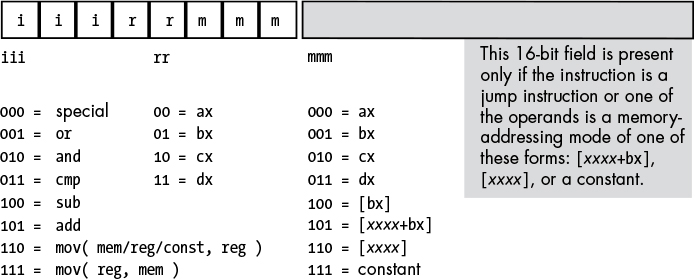
Figure 10-3: Basic Y86 instruction encoding
The basic instruction is either 1 or 3 bytes long, and its opcode consists of a single byte containing three fields. The first field, consisting of the HO 3 bits, defines the instruction, and these 3 bits provide eight possible combinations. As there are 18 different Y86 instructions, we’ll have to pull some tricks to handle the remaining 10 instructions.
10.3.4.1 Eight Generic Y86 Instructions
As you can see in Figure 10-3, seven of the eight basic opcodes encode the or, and, cmp, sub, and add instructions, as well as both versions of the mov instruction. The eighth, 000, is an expansion opcode. This special instruction class, which we’ll return to shortly, provides a mechanism that allows us to expand the set of available instructions.
To determine the full opcode for a particular instruction, you simply select the appropriate bits for the iii, rr, and mmm fields (identified in Figure 10-3). The rr field contains the destination register (except for the version of the mov instruction whose iii field is 111), and the mmm field encodes the source register. For example, to encode the mov(bx, ax); instruction you would select iii = 110 (mov(reg, reg);), rr = 00 (ax), and mmm = 001 (bx). This produces the 1-byte instruction %11000001, or $c0.
Some Y86 instructions are larger than 1 byte. To illustrate why this is necessary, take, for example, the instruction mov([1000], ax);, which loads the AX register with the value stored at memory location $1000. The encoding for the opcode is %11000110, or $c6. However, the encoding for the mov([2000], ax); instruction is also $c6. Clearly these two instructions do different things: one loads the AX register from memory location $1000, while the other loads the AX register from memory location $2000.
In order to differentiate between instructions that encode an address using the [xxxx] or [xxxx+bx] addressing modes, or to encode a constant using the immediate addressing mode, you must append the 16-bit address or constant to the instruction’s opcode. Within this 16-bit address or constant, the LO byte follows the opcode in memory and the HO byte follows the LO byte. So, the 3-byte encoding for mov([1000], ax); would be $c6, $00, $10, and the 3-byte encoding for mov([2000], ax); would be $c6, $00, $20.
10.3.4.2 The Special Expansion Opcode
The special opcode in Figure 10-3 allows the Y86 CPU to expand the set of available instructions that can be encoded using a single byte. This opcode handles several zero- and one-operand instructions, as shown in Figures 10-4 and 10-5.
Figure 10-4 shows the encodings of four one-operand instruction classes. The first 2-bit encoding for the rr field, %00, further expands the instruction set by providing a way to encode the zero-operand instructions shown in Figure 10-5. Five of these instructions are illegal instruction opcodes; the three valid opcodes are the halt instruction, which terminates program execution; the get instruction, which reads a hexadecimal value from the user and stores it in the AX register; and the put instruction, which outputs the value in the AX register.
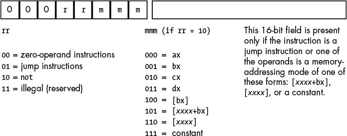
Figure 10-4: Single-operand instruction encodings (iii = %000)
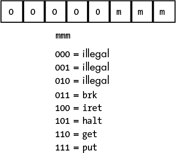
Figure 10-5: Zero-operand instruction encodings (iii = %000 and rr = %00)
The second 2-bit encoding for the rr field, %01, is also part of an expansion opcode that provides all the Y86 jump instructions (see Figure 10-6). The third rr field encoding, %10, is for the not instruction. The fourth rr field encoding is currently unassigned. Any attempt to execute an opcode with an iii field encoding of %000 and an rr field encoding of %11 will halt the processor with an illegal instruction error. As previously discussed, CPU designers often reserve unassigned opcodes like this one so they can extend the instruction set in the future (as Intel did when moving from the 80286 processor to the 80386 or from the 32-bit x86 processors to the 64-bit x86-64 processors).
The seven jump instructions in the Y86 instruction set all take the form jxx address;. The jmp instruction copies the 16-bit address value that follows the opcode into the instruction pointer register, causing the CPU to fetch the next instruction from the target address of the jmp. The remaining six instructions—ja, jae, jb, jbe, je, and jne—test some condition and, if it is true, copy the address value into the instruction pointer register. The eighth opcode, %00001111, is another illegal opcode. These encodings are shown in Figure 10-6.
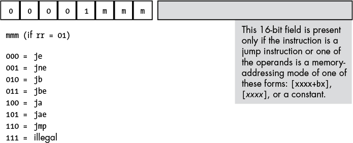
Figure 10-6: Jump instruction encodings
10.3.5 Examples of Encoding Y86 Instructions
The Y86 processor does not execute instructions as human-readable strings of characters like mov(ax, bx);. Instead, it fetches instructions as bit patterns, such as $c1, from memory, then decodes and executes those bit patterns. Human-readable instructions like mov(ax, bx); and add(5, cx); must first be converted into binary representation, or machine code. This section will explore this conversion.
10.3.5.1 The add Instruction
We’ll start our conversion with a very simple example, the add(cx, dx); instruction. Once you’ve chosen the instruction, you look it up in one of the opcode figures from the previous section. The add instruction is in the first group (see Figure 10-3) and has an iii field of %101. The source operand is cx, so the mmm field is %010. The destination operand is dx, so the rr field is %11. Merging these bits produces the opcode %10111010, or $ba (see Figure 10-7).
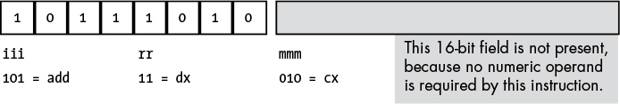
Figure 10-7: Encoding the add( cx, dx ); instruction
Now consider the add(5, ax) instruction. Because it has an immediate source operand (a constant), the mmm field will be %111 (see Figure 10-3). The destination register operand is ax (%00), and the instruction class field is %101, so the full opcode becomes %10100111, or $a7. However, we’re not finished yet. We also have to include the 16-bit constant $0005 as part of the instruction, with the LO byte of the constant following the opcode, and the HO byte of the constant following its LO byte, because the bytes are arranged in little-endian order. So, the sequence of bytes in memory, from lowest address to highest address, is $a7, $05, $00 (see Figure 10-8).
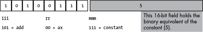
Figure 10-8: Encoding the add( 5, ax ); instruction
The add([2ff+bx], cx) instruction also contains a 16-bit constant that is the displacement portion of the indexed addressing mode. To encode this instruction, we use the following field values: iii = %101, rr = %10, and mmm = %101. This produces the opcode byte %10110101, or $b5. The complete instruction also requires the constant $2ff, so the full instruction is the 3-byte sequence $b5, $ff, $02 (see Figure 10-9).
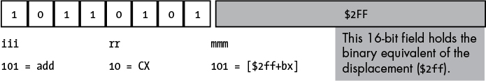
Figure 10-9: Encoding the add( [$2ff+bx], cx ); instruction
Now consider add([1000], ax). This instruction adds the 16-bit contents of memory locations $1000 and $1001 to the value in the AX register. Once again, iii = %101 for the add instruction. The destination register is ax, so rr = %00. Finally, the addressing mode is the displacement-only addressing mode, so mmm = %110. This forms the opcode %10100110, or $a6. The complete instruction is 3 bytes long, because it must also encode the displacement (address) of the memory location in the 2 bytes following the opcode. Therefore, the complete 3-byte sequence is $a6, $00, $10 (see Figure 10-10).
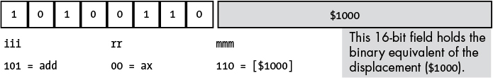
Figure 10-10: Encoding the add( [1000], ax ); instruction
The last addressing mode to consider is the register indirect addressing mode, [bx]. The add([bx],bx) instruction uses the following encoded values: mmm = %101, rr = %01 (bx), and mmm = %100 ([bx]). Because the value in the BX register completely specifies the memory address, there’s no need to attach a displacement field to the instruction’s encoding. Hence, this instruction is only 1 byte long (see Figure 10-11).
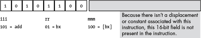
Figure 10-11: Encoding the add([bx], bx); instruction
You use a similar approach to encode the sub, cmp, and, and or instructions. The only difference between encoding these instructions and the add instruction is the value you use for the iii field in the opcode.
10.3.5.2 The mov Instruction
The Y86 mov instruction is special, because it comes in two forms. The only difference between the encoding of the add instruction and the encoding of the mov instruction’s first form (iii = %110) is the iii field. This form of mov copies either a constant or data from the register or memory address specified by the mmm field into the destination register specified by the rr field.
The second form of the mov instruction (iii = %111) copies data from the source register specified by the rr field to a destination memory location specified by the mmm field. In this form of the mov instruction, the source and destination meanings of the rr and mmm fields are reversed: rr is the source field and mmm is the destination field. Another difference between the two forms of mov is that in its second form, the mmm field may contain only the values %100 ([bx]), %101 ([disp+bx]), and %110 ([disp]). The destination values can’t be any of the registers encoded by mmm field values in the range %000 through %011 or a constant encoded by an mmm field of %111. These encodings are illegal because the first form of the mov handles cases with a register destination, and because storing data into a constant doesn’t make any sense.
10.3.5.3 The not Instruction
The not instruction is the only instruction with a single memory/register operand that the Y86 processor supports. It has the following syntax:
not(reg);
or:
not(address);
where address represents one of the memory addressing modes ([bx], [disp+bx], or [disp]). You may not specify a constant operand for the not instruction.
Because not has only a single operand, it needs only the mmm field to encode that operand. An iii field of %000 and an rr field of %10 identify the not instruction. In fact, whenever the iii field contains 0, the CPU knows that it has to decode bits beyond the iii field to identify the instruction. In this case, the rr field specifies whether we’ve encoded not or one of the other specially encoded instructions.
To encode an instruction like not(ax), specify %000 for the iii field and %10 for the rr field, then encode the mmm field the same way you would encode it for the add instruction. Because mmm = %000 for AX, not(ax) would be encoded as %00010000, or $10 (see Figure 10-12).
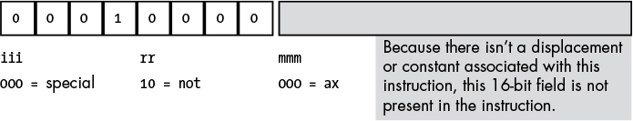
Figure 10-12: Encoding the not(AX); instruction
The not instruction does not allow an immediate, or constant, operand, so the opcode %00010111 ($17) is an illegal opcode.
10.3.5.4 The Jump Instructions
The Y86 jump instructions also use the special encoding, meaning that the iii field for jump instructions is always %000. These instructions are always 3 bytes long. The first byte, the opcode, specifies which jump instruction to execute, and the next 2 bytes specify the address in memory to which the CPU transfers control (if the condition is met, in the case of the conditional jumps). There are seven different Y86 jump instructions, six conditional jumps, and one unconditional jump, jmp. All seven of these instructions set iii = %000 and rr = %01, so they differ only by their mmm fields. The eighth possible opcode, with an mmm field value of %111, is an illegal opcode (see Figure 10-6).
Encoding these instructions is relatively straightforward. Picking the instruction you want to encode completely determines the opcode. The opcode values fall in the range $08 through $0e ($0f is the illegal opcode).
The only field that requires some thought is the 16-bit operand that follows the opcode. This field holds the address of the target instruction to which the unconditional jump always transfers, and to which the conditional jumps transfer if the transfer condition is true. To properly encode this 16-bit operand, you must know the address of the opcode byte of the target instruction. If you’ve already converted the target instruction to binary form and stored it into memory, you’re all set—just specify the target instruction’s address as the sole operand of the jump instruction. On the other hand, if you haven’t yet written, converted, and placed the target instruction into memory, knowing its address would seem to require a bit of divination. Fortunately, you can figure it out by computing the lengths of all the instructions between the current jump instruction you’re encoding and the target instruction—but unfortunately, this is an arduous task.
The best way to calculate the distance is to write all your instructions down on paper, compute their lengths (which is easy, because all instructions are either 1 or 3 bytes long depending on whether they have a 16-bit operand), and then assign an appropriate address to each instruction. Once you’ve done this, you’ll know the starting address for each instruction, and you can put target address operands into your jump instructions as you encode them.
10.3.5.5 The Zero-Operand Instructions
The remaining instructions, the zero-operand instructions, are the easiest to encode. Because they have no operands, they are always 1 byte long. These instructions always have iii = %000 and rr = %00, and mmm specifies the particular instruction opcode (see Figure 10-5). Note that the Y86 CPU leaves five of these instructions undefined (so we can use these opcodes for future expansion).
10.3.6 Extending the Y86 Instruction Set
The Y86 CPU is a trivial CPU, suitable only for demonstrating how to encode machine instructions. However, as with any good CPU, the Y86 design allows for expansion by adding new instructions.
You can extend the number of instructions in a CPU’s instruction set by using either undefined or illegal opcodes. So, because the Y86 CPU has several illegal and undefined opcodes, we’ll use them to expand the instruction set.
Using undefined opcodes to define new instructions works best when there are undefined bit patterns within an opcode group, and the new instruction you want to add falls into that same group. For example, the opcode %00011mmm falls into the same group as the not instruction, which also has an iii field value of %000. If you decided that you really needed a neg (negate) instruction, using the %00011mmm opcode makes sense because you’d probably expect neg to use the same syntax as the not instruction. Likewise, if you want to add a zero-operand instruction to the instruction set, Y86 has five undefined zero-operand instructions for you to choose from (%0000000..%00000100; see Figure 10-5). You’d just appropriate one of these opcodes and assign your instruction to it.
Unfortunately, the Y86 CPU doesn’t have many illegal opcodes available. For example, if you wanted to add the shl (shift left), shr (shift right), rol (rotate left), and ror (rotate right) instructions as single-operand instructions, there’s not enough space within the group of single-operand instruction opcodes to do so (only %00011mmm is currently open). Likewise, there are no two-operand opcodes open, so if you wanted to add an xor (exclusive OR) instruction or some other two-operand instruction, you’d be out of luck.
A common way to handle this dilemma, and one the Intel designers have employed, is to use one of the undefined opcodes as a prefix opcode byte. For example, the opcode $ff is illegal (it corresponds to a mov(dx, constant) instruction), but we can use it as a special prefix byte to further expand the instruction set (see Figure 10-13).4
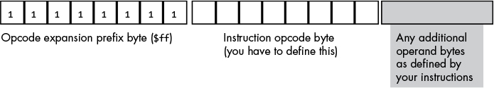
Figure 10-13: Using a prefix byte to extend the instruction set
Whenever the CPU encounters a prefix byte in memory, it reads and decodes the next byte in memory as the actual opcode. However, it doesn’t treat the second byte as it would a standard opcode that did not follow a prefix byte. Instead, it allows the CPU designer to create a completely new opcode scheme, independent of the original instruction set. A single-expansion opcode byte allows CPU designers to add up to 256 more instructions to the instruction set. For even more instructions, designers can use additional illegal opcode bytes (in the original instruction set) to add still more expansion opcodes, each with its own independent instruction set; or they can follow the opcode expansion prefix byte with a 2-byte opcode (yielding up to 65,536 new instructions); or they can execute any other scheme they can dream up.
Of course, one big drawback of this approach is that it increases the size of the new instructions by 1 byte, because each instruction now requires the prefix byte as part of the opcode. This also increases the cost of the circuitry (since decoding prefix bytes and multiple instruction sets is fairly complex), so you don’t want to use this scheme for the basic instruction set. Nevertheless, it is a good way to expand the instruction set when you’ve run out of opcodes.
10.4 Encoding 80x86 Instructions
The Y86 processor is simple to understand; we can easily encode instructions by hand for it, and it’s a great vehicle for learning how to assign opcodes. It’s also a purely hypothetical device intended only as a teaching tool. So, it’s time to take a look at the machine instruction format for a real CPU: the 80x86. After all, the programs you write will run on a real CPU, so to fully appreciate what your compilers are doing with your code—so you can choose the best statements and data structures when writing that code—you need to understand how real instructions are encoded.
Even if you’re using a different CPU, studying the 80x86 instruction encoding is helpful. They don’t call the 80x86 a complex instruction set computer (CISC) chip for nothing. Although more complex instruction encodings do exist, no one would challenge the assertion that it’s one of the more complex instruction sets in common use today. Therefore, exploring it will provide valuable insight into the operation of other real-world CPUs.
The generic 80x86 32-bit instruction takes the form shown in Figure 10-14.5
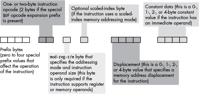
Figure 10-14: 80x86 32-bit instruction encoding
NOTE
Although this diagram seems to imply that instructions can be up to 16 bytes long, 15 bytes is actually the limit.
The prefix bytes are not the same as the opcode expansion prefix byte that we discussed in the previous section. Instead, the 80x86 prefix bytes modify the behavior of existing instructions. An instruction may have a maximum of four prefix bytes attached to it, but the 80x86 supports more than four different prefix values. The behaviors of many prefix bytes are mutually exclusive, and the results of an instruction will be undefined if you prepend a pair of mutually exclusive prefix bytes to it. We’ll take a look at a couple of these prefix bytes in a moment.
The (32-bit) 80x86 supports two basic opcode sizes: a standard 1-byte opcode and a 2-byte opcode consisting of a $0f opcode expansion prefix byte and a second byte specifying the actual instruction. One way to think of this opcode expansion prefix byte is as an 8-bit extension of the iii field in the Y86 encoding. This enables the encoding of up to 512 different instruction classes, although the 80x86 doesn’t yet use them all. In reality, various instruction classes use certain bits in this opcode expansion prefix byte for decidedly non-instruction-class purposes. For example, consider the add instruction opcode shown in Figure 10-15.
Bit 1 (d) specifies the direction of the transfer. If this bit is 0, then the destination operand is a memory location, such as in add(al, [ebx]);. If this bit is 1, the destination operand is a register, as in add([ebx], al);.
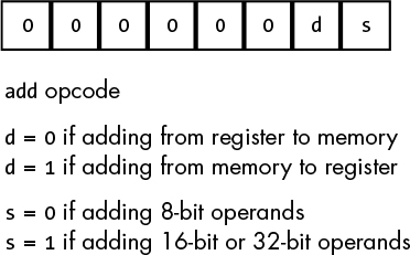
Figure 10-15: 80x86 add opcode
Bit 0 (s) specifies the size of the operands the add instruction operates upon. There’s a problem here, however. The 32-bit 80x86 family supports up to three different operand sizes: 8-bit operands, 16-bit operands, and 32-bit operands. With a single size bit, the instruction can encode only two of these three different sizes. In 32-bit operating systems, the vast majority of operands are either 8 bits or 32 bits, so the 80x86 CPU uses the size bit in the opcode to encode those sizes. For 16-bit operands, which occur less frequently than 8-bit or 32-bit operands, Intel uses a special opcode prefix byte to specify the size. As long as instructions that have 16-bit operands occur less than one out of every eight instructions (which is generally the case), this is more compact than adding another bit to the instruction’s size. Using a size prefix byte allowed Intel’s designers to extend the number of operand sizes without having to change the instruction encoding inherited from the original 16-bit processors in this CPU family.
Note that the AMD/Intel 64-bit architectures go even crazier with opcode prefix bytes. However, the CPU operates in a special 64-bit mode; effectively, the 64-bit 80x86 CPUs (often called the X86-64 CPUs) have two completely different instruction sets, each with its own encoding. The X86-64 CPUs can switch between 64- and 32-bit modes to handle programs written in either of the different instruction sets. The encoding in this chapter covers the 32-bit variant; see the Intel or AMD documentation for details on the 64-bit version.
10.4.1 Encoding Instruction Operands
The mod-reg-r/m byte (see Figure 10-14) provides the encoding for instruction operands by specifying the base addressing mode used to access them as well as their size. This byte contains the fields shown in Figure 10-16.
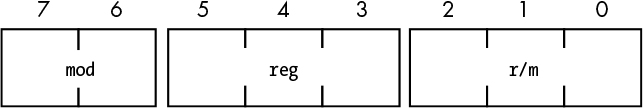
Figure 10-16: mod-reg-r/m byte
The reg field almost always specifies an 80x86 register. However, depending on the instruction, the register specified by reg can be either the source or the destination operand. To distinguish between the two, many instructions’ upcodes include the d (direction) field, which contains a value of 0 when reg is the source and a value of 1 when it’s the destination operand.
This field uses the 3-bit register encodings found in Table 10-1. As just discussed, the size bit in the instruction’s opcode indicates whether the reg field specifies an 8- or 32-bit register (when operating under a modern, 32-bit operating system). To make the reg field specify a 16-bit register, you must set the size bit in the opcode to 1, as well as adding an extra prefix byte.
Table 10-1: reg Field Encodings
reg value |
Register if data size is 8 bits |
Register if data size is 16 bits |
Register if data size is 32 bits |
%000 |
al |
ax |
eax |
%001 |
cl |
cx |
ecx |
%010 |
dl |
dx |
edx |
%011 |
bl |
bx |
ebx |
%100 |
ah |
sp |
esp |
%101 |
ch |
bp |
ebp |
%110 |
dh |
si |
esi |
%111 |
bh |
di |
edi |
With the d bit in the opcode of a two-operand instruction indicating whether the reg field contains the source or destination operand, the mod and r/m fields together specify the other of the two operands. In the case of a single-operand instruction like not or neg, the reg field contains an opcode extension, and mod and r/m combine to specify the only operand. The operand addressing modes specified by the mod and r/m fields are listed in Tables 10-2 and 10-3.
Table 10-2: mod Field Encodings
mod |
Description |
%00 |
Specifies register-indirect addressing mode (with two exceptions: scaled-index [sib] addressing modes with no displacement operand when r/m = %100; and displacement-only addressing mode when r/m = %101). |
%01 |
Specifies that a 1-byte signed displacement follows the addressing mode byte(s). |
%10 |
Specifies that a 1-byte signed displacement follows the addressing mode byte(s). |
%11 |
Specifies direct register access. |
mod |
r/m |
Addressing mode |
%00 |
%000 |
[eax] |
%01 |
%000 |
[eax+disp8] |
%10 |
%000 |
[eax+disp32] |
%11 |
%000 |
al, ax, or eax |
%00 |
%001 |
[ecx] |
%01 |
%001 |
[ecx+disp8] |
%10 |
%001 |
[ecx+disp32] |
%11 |
%001 |
cl, cx, or ecx |
%00 |
%010 |
[edx] |
%01 |
%010 |
[edx+disp8] |
%10 |
%010 |
[edx+disp32] |
%11 |
%010 |
dl, dx, or edx |
%00 |
%011 |
[ebx] |
%01 |
%011 |
[ebx+disp8] |
%10 |
%011 |
[ebx+disp32] |
%11 |
%011 |
bl, bx, or ebx |
%00 |
%100 |
Scaled-index (sib) mode |
%01 |
%100 |
sib + disp8 mode |
%10 |
%100 |
sib + disp32 mode |
%11 |
%100 |
ah, sp, or esp |
%00 |
%101 |
Displacement-only mode (32-bit displacement) |
%01 |
%101 |
[ebp+disp8] |
%10 |
%101 |
[ebp+disp32] |
%11 |
%101 |
ch, bp, or ebp |
%00 |
%110 |
[esi] |
%01 |
%110 |
[esi+disp8] |
%10 |
%110 |
[esi+disp32] |
%11 |
%110 |
dh, si, or esi |
%00 |
%111 |
[edi] |
%01 |
%111 |
[edi+disp8] |
%10 |
%111 |
[edi+disp32] |
%11 |
%111 |
bh, di, or edi |
There are a couple of interesting things to note about Tables 10-2 and 10-3. First, there are two different forms of the [reg+disp] addressing modes: one form with an 8-bit displacement and one form with a 32-bit displacement. Addressing modes whose displacement falls in the range –128 through +127 require only a single byte after the opcode to encode the displacement. Instructions with a displacement that falls within this range will be shorter and sometimes faster than instructions whose displacement values are not within this range and thus require 4 bytes after the opcode.
The second thing to note is that there is no [ebp] addressing mode. If you look at the entry in Table 10-3 where this addressing mode logically belongs (where r/m is %101 and mod is %00), you’ll find that its slot is occupied by the 32-bit displacement-only addressing mode. The basic encoding scheme for addressing modes didn’t allow for a displacement-only addressing mode, so Intel “stole” the encoding for [ebp] and used that for the displacement-only mode. Fortunately, anything you can do with the [ebp] addressing mode you can also do with the [ebp+disp8] addressing mode by setting the 8-bit displacement to 0. While such an instruction is a bit longer than it would otherwise need to be if the [ebp] addressing mode existed, the same capabilities are still there. Intel wisely chose to replace this particular register-indirect addressing mode, anticipating that programmers would use it less often than the other register-indirect addressing modes.
Another thing you’ll notice missing from this table are addressing modes of the form [esp], [esp+disp8], and [esp+disp32]. Intel’s designers borrowed the encodings for these three addressing modes to support the scaled-index addressing modes they added to their 32-bit processors in the 80x86 family.
If r/m = %100 and mod = %00, this specifies an addressing mode of the form [reg132+reg232*n]. This scaled-index addressing mode computes the final address in memory as the sum of reg2 multiplied by n (n = 1, 2, 4, or 8) and reg1. Programs most often use this addressing mode when reg1 is a pointer holding the base address of an array of bytes (n = 1), words (n = 2), double words (n = 4), or quad words (n = 8), and reg2 holds the index into that array.
If r/m = %100 and mod = %01, this specifies an addressing mode of the form [reg132+reg232*n+disp8]. This scaled-index addressing mode computes the final address in memory as the sum of reg2 multiplied by n (n = 1, 2, 4, or 8), reg1, and the 8-bit signed displacement (sign-extended to 32 bits). Programs most often use this addressing mode when reg1 is a pointer holding the base address of an array of records, reg2 holds the index into that array, and disp8 provides the offset to a desired field in the record.
If r/m = %100 and mod = %10, this specifies an addressing mode of the form [reg132+reg232*n+disp32]. This scaled-index addressing mode computes the final address in memory as the sum of reg2 multiplied by n (n = 1, 2, 4, or 8), reg1, and the 32-bit signed displacement. Programs most often use this addressing mode to index into static arrays of bytes, words, double words, or quad words.
If values corresponding to one of the sib modes appear in the mod and r/m fields, the addressing mode is a scaled-index addressing mode with a second byte (the sib) following the mod-reg-r/m byte, though don’t forget that the mod field still specifies a displacement size of 0, 1, or 4 bytes. Figure 10-17 shows the layout of this extra sib, and Tables 10-4, 10-5, and 10-6 explain the values for each of the sib fields.
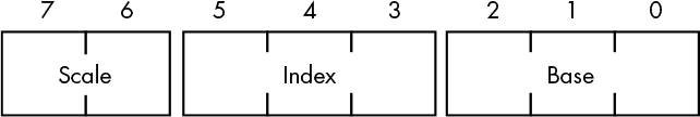
Figure 10-17: The sib (scaled-index byte) layout
Scale value |
Index * scale value |
%00 |
Index * 1 |
%01 |
Index * 2 |
%10 |
Index * 4 |
%11 |
Index * 8 |
Table 10-5: Register Values for sib Encoding
Index value |
Register |
%000 |
EAX |
%001 |
ECX |
%010 |
EDX |
%011 |
EBX |
%100 |
Illegal |
%101 |
EBP |
%110 |
ESI |
%111 |
EDI |
Table 10-6: Base Register Values for sib Encoding
Base value |
Register |
%000 |
EAX |
%001 |
ECX |
%010 |
EDX |
%011 |
EBX |
%100 |
ESP |
%101 |
Displacement only if mod = %00, EBP if mod = %01 or %10 |
%110 |
ESI |
%111 |
EDI |
The mod-reg-r/m and sib bytes are complex and convoluted, no question about that. The reason is that Intel reused its 16-bit addressing circuitry when it switched to the 32-bit format rather than simply abandoning it at that point. There were good hardware reasons for retaining it, but the result is a complex scheme for specifying addressing modes. As you can imagine, things got even worse when Intel and AMD developed the x86-64 architecture.
Note that if the r/m field of the mod-reg-r/m byte contains %100 and mod does not contain %11, the addressing mode is a sib mode rather than the expected [esp], [esp+disp8], or [esp+disp32] mode. In this case the compiler or assembler will emit an extra sib byte immediately following the mod-reg-r/m byte. Table 10-7 lists the various combinations of legal scaled-index addressing modes on the 80x86.
In each of the addressing modes listed in Table 10-7, the mod field of the mod-reg-r/m byte specifies the size of the displacement (0, 1, or 4 bytes). The base and index fields of the sib specify the base and index registers, respectively. Note that this addressing mode does not allow the use of ESP as an index register. Presumably, Intel left this particular mode undefined to allow for extending the addressing modes to 3 bytes in a future version of the CPU, although doing so seems a bit extreme.
Just as the mod-reg-r/m encoding replaced the [ebp] addressing mode with a displacement-only mode, the sib addressing format replaces the [ebp+index*scale] mode with a displacement-plus index mode (that is, no base register). If it turns out that you really need to use the [ebp+index*scale] addressing mode, you’ll have to use the [disp8+ebp+index*scale] mode instead, specifying a 1-byte displacement value of 0.
Table 10-7: The Scaled-Index Addressing Modes
mod |
Index |
Legal scaled-index addressing modes6 |
%00 Base ° %101 |
%000 |
[base32+eax*n] |
%001 |
[base32+ecx*n] |
|
%010 |
[base32+edx*n] |
|
%011 |
[base32+ebx*n] |
|
%100 |
n/a7 |
|
%101 |
[base32+ebp*n] |
|
%110 |
[base32+esi*n] |
|
%111 |
[base32+edi*n] |
|
%00 Base = %1018 |
%000 |
[disp32+eax*n] |
%001 |
[disp32+ecx*n] |
|
%010 |
[disp32+edx*n] |
|
%011 |
[disp32+ebx*n] |
|
%100 |
n/a |
|
%101 |
[disp32+ebp*n] |
|
%110 |
[disp32+esi*n] |
|
%111 |
[disp32+edi*n] |
|
%01 |
%000 |
[disp8+base32+eax*n] |
%001 |
[disp8+base32+ecx*n] |
|
%010 |
[disp8+base32+edx*n] |
|
%011 |
[disp8+base32+ebx*n] |
|
%100 |
n/a |
|
%101 |
[disp8+base32+ebp*n] |
|
%110 |
[disp8+base32+esi*n] |
|
%111 |
[disp8+base32+edi*n] |
|
%10 |
%000 |
[disp32+base32+eax*n] |
%001 |
[disp32+base32+ecx*n] |
|
%010 |
[disp32+base32+edx*n] |
|
%011 |
[disp32+base32+ebx*n] |
|
%100 |
n/a |
|
%101 |
[disp32+base32+ebp*n] |
|
%110 |
[disp32+base32+esi*n] |
|
%111 |
[disp32+base32+edi*n] |
10.4.2 Encoding the add Instruction
To help you figure out how to encode an instruction using this complex scheme, let’s look at an example of the 80x86 add instruction using various addressing modes. The add opcode is either $00, $01, $02, or $03, depending on its direction and size bits (see Figure 10-15). Figures 10-18 through 10-25 show how to encode various forms of the add instruction using different addressing modes.
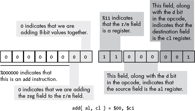
Figure 10-18: Encoding the add(al, cl); instruction
There is an interesting side effect of the mod-reg-r/m organization and direction bit: some instructions have two different legal opcodes. For example, we could also encode the add(al, cl); instruction shown in Figure 10-18 as $02, $c8 by reversing the positions of the AL and CL registers in the reg and r/m fields and then setting the d bit (bit 1) in the opcode to 1. This applies to all instructions with two register operands and a direction bit, such as the add(eax, ecx); instruction in Figure 10-19, which can also be encoded as $03, $c8.
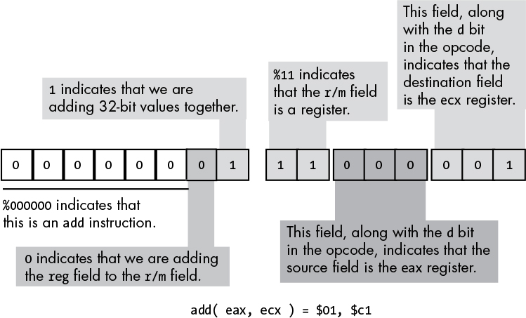
Figure 10-19: Encoding the add(eax, ecx); instruction
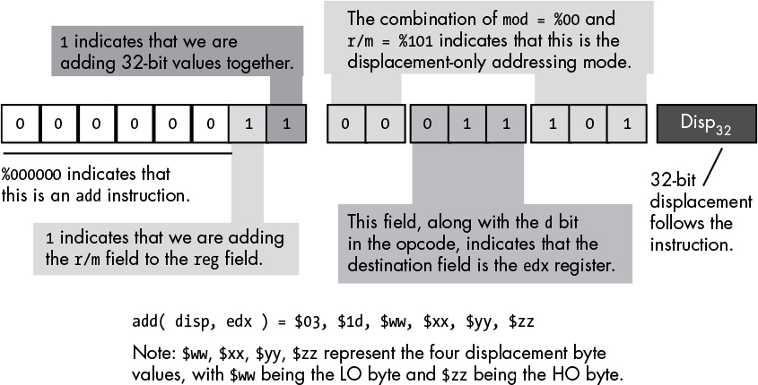
Figure 10-20: Encoding the add(disp, edx); instruction
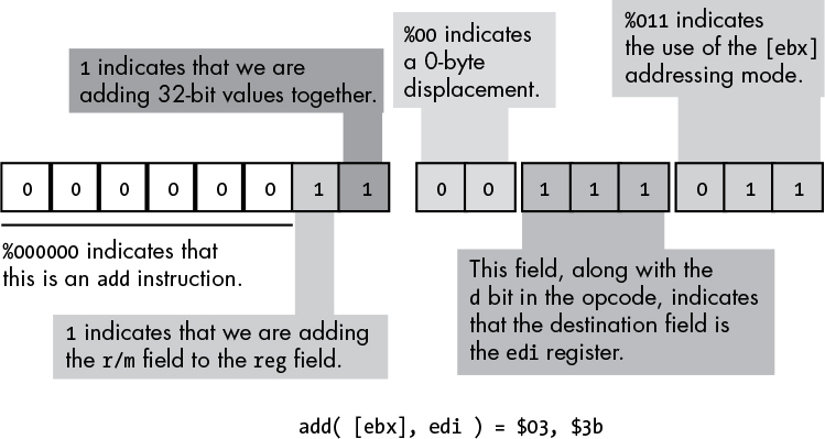
Figure 10-21: Encoding the add([ebx], edi); instruction
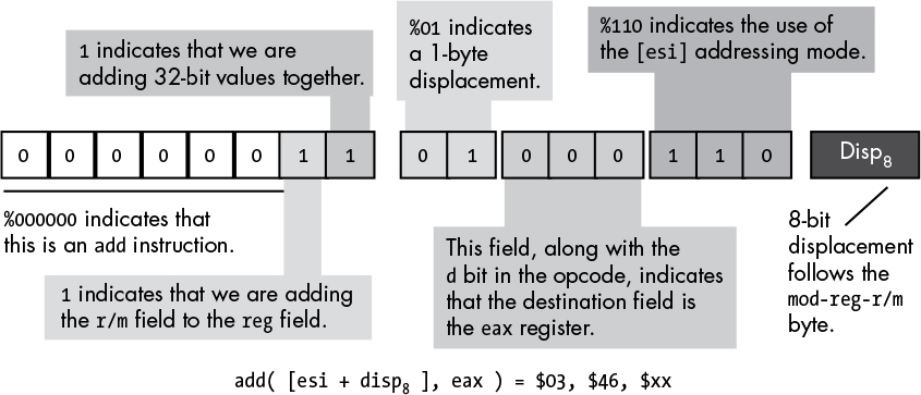
Figure 10-22: Encoding the add([esi+disp8], eax); instruction
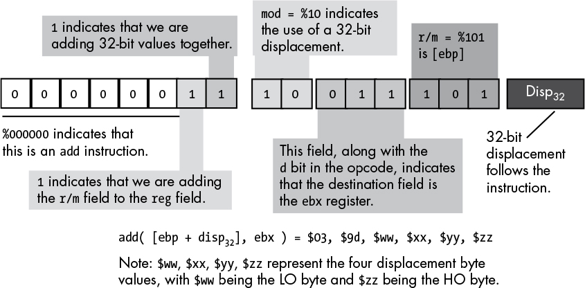
Figure 10-23: Encoding the add([ebp+disp32], ebx); instruction
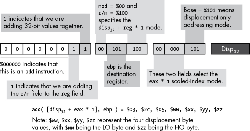
Figure 10-24: Encoding the add([disp32+eax*1], ebp); instruction
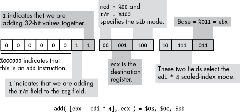
Figure 10-25: Encoding the add([ebx+edi*4], ecx); instruction
10.4.3 Encoding Immediate (Constant) Operands on the x86
You may have noticed that the mod-reg-r/m and sib bytes don’t contain any bit combinations you can use to specify that an instruction contains an immediate operand. The 80x86 uses a completely different opcode to specify an immediate operand. Figure 10-26 shows the basic encoding for an add immediate instruction.
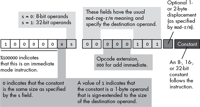
Figure 10-26: Encoding an add immediate instruction
There are three major differences between the encoding of the add immediate instruction and the standard add instruction. First, and most important, the opcode has a 1 in the HO bit position. This tells the CPU that the instruction has an immediate constant. This change alone, however, does not tell the CPU that it must execute an add instruction, as you’ll see shortly.
The second difference is that there’s no direction bit in the opcode. This makes sense because you cannot specify a constant as a destination operand. Therefore, the destination operand is always the location specified by the mod and r/m bits in the mod-reg-r/m field.
In place of the direction bit, the opcode has a sign-extension (x) bit. For 8-bit operands, the CPU ignores the sign-extension bit. For 16-bit and 32-bit operands, the sign-extension bit specifies the size of the constant following the add instruction. If the sign-extension bit contains 0, the constant is already the same size as the operand (either 16 or 32 bits). If the sign-extension bit contains 1, the constant is a signed 8-bit value, and the CPU sign-extends this value to the appropriate size before adding it to the operand. This little trick often makes programs much shorter, because you commonly add small constants to 16- or 32-bit destination operands.
The third difference between the add immediate and the standard add instruction is the meaning of the reg field in the mod-reg-r/m byte. Because the instruction implies that the source operand is a constant, and the mod-r/m fields specify the destination operand, the instruction does not need to use the reg field to specify an operand. Instead, the 80x86 CPU uses these 3 bits as an opcode extension. For the add immediate instruction, these 3 bits must contain 0, and another bit pattern would correspond to a different instruction.
When a constant is added to a memory location, any displacement associated with that memory location immediately precedes the constant data in the instruction sequence.
10.4.4 Encoding 8-, 16-, and 32-Bit Operands
When designing the 8086, Intel used one opcode bit (s) to specify whether the operand sizes were 8 or 16 bits. Later, when it extended the 80x86 architecture to 32 bits with the introduction of the 80386, Intel had a problem: with this single operand size bit, it could encode only two sizes, but it needed to encode three (8, 16, and 32 bits). To solve this problem, Intel used an operand-size prefix byte.
Intel studied its instruction set and concluded that in a 32-bit environment, programs were likely to use 8-bit and 32-bit operands far more often than 16-bit operands. Therefore, it decided to let the size bit (s) in the opcode select between 8- and 32-bit operands, as described in the previous sections. Although modern 32-bit programs don’t use 16-bit operands very often, they do need them now and then. So, Intel lets you prefix a 32-bit instruction with the operand-size prefix byte, whose value is $66, and this prefix byte tells the CPU that the operands contain 16-bit data rather than 32-bit data.
You do not have to explicitly add an operand-size prefix byte to your 16-bit instructions; the assembler or compiler takes care of this automatically for you. However, do keep in mind that whenever you use a 16-bit object in a 32-bit program, the instruction is 1 byte longer because of the prefix value. Therefore, you should be careful about using 16-bit instructions if size and, to a lesser extent, speed are important.
10.4.5 Encoding 64-Bit Operands
When running in 64-bit mode, Intel and AMD x84-64 processors use special opcode prefix bytes to specify 64-bit registers. There are 16 REX opcode bytes that handle 64-bit operands and addressing modes. Because there weren’t 16 single-byte opcodes available, AMD (who designed the instruction set) chose to repurpose 16 existing opcodes (the 1-byte opcode variants for the inc(reg) and dec(reg) instructions). There are still 2-byte variants of these instructions, so rather than eliminating the instructions altogether, AMD just removed the 1-byte versions. However, standard 32-bit code (a lot of which certainly uses those 1-byte increment and decrement instructions) can no longer run on the 64-bit model. That’s why AMD and Intel introduced new 32-bit and 64-bit operation modes—so the CPUs could run both older 32-bit code and newer 64-bit code on the same piece of silicon.
10.4.6 Alternate Encodings for Instructions
As noted earlier in this chapter, one of Intel’s primary design goals for the 80x86 was to create an instruction set that allowed programmers to write very short programs in order to save memory, which was precious at the time. One way Intel did this was to create alternative encodings of some very commonly used instructions. These alternative instructions were shorter than their standard counterparts, and Intel hoped that programmers would make extensive use of the shorter versions, thereby creating shorter programs.
A good example of these alternative instructions are the add(constant, accumulator); instructions, where the accumulator is al, ax, or eax. The 80x86 provides 1-byte opcodes for add(constant, al); and add(constant, eax);, which are $04 and $05, respectively. With a 1-byte opcode and no mod-reg-r/m byte, these instructions are 1 byte shorter than their standard add immediate counterparts. The add(constant, ax); instruction requires an operand-size prefix, so its opcode is effectively 2 bytes. However, this is still 1 byte shorter than the corresponding standard add immediate.
You don’t have to specify anything special to use these instructions. Any decent assembler or compiler will automatically choose the shortest possible instruction it can use when translating your source code into machine code. However, you should note that Intel provides alternative encodings only for the accumulator registers. Therefore, if you have a choice of several instructions to use and the accumulator registers are among these choices, the AL, AX, and EAX registers are often your best bet. However, this option is usually available only to assembly language programmers.
10.5 Implications of Instruction Set Design to the Programmer
Only by knowing the computer’s architecture and, in particular, how the CPU encodes machine instructions, can you make the most efficient use of the machine’s instructions. By studying instruction set design, you can gain a clear understanding of the following:
- Why some instructions are shorter than others
- Why some instructions are faster than others
- Which constant values the CPU can handle efficiently
- Whether constants are more efficient than memory locations
- Why certain arithmetic and logical operations are more efficient than others
- Which types of arithmetic expressions are more easily translated into machine code than other types
- Why code is less efficient if it transfers control over a large distance in the object code
. . . and so on.
By studying instruction set design, you become more aware of the implications of the code you write (even in an HLL) in terms of efficient operation on the CPU. Armed with this knowledge, you’ll be better equipped to write great code.
10.6 For More Information
Hennessy, John L., and David A. Patterson. Computer Architecture: A Quantitative Approach. 5th ed. Waltham, MA: Elsevier, 2012.
Hyde, Randall. The Art of Assembly Language. 2nd ed. San Francisco: No Starch Press, 2010.
Intel. “Intel® 64 and IA-32 Architectures Software Developer Manuals.” Last updated November 11, 2019. https://software.intel.com/en-us/articles/intel-sdm/.