
Modified Carbon Nanostructures for Display and Energy Storage |
CONTENTS
8.3.2 Intercalation of MoO3–MWCNT Nanocomposites
Carbon nanostructures have been gaining considerable interest over the last three decades after the discovery of fullerenes in 1985 showed the possibility of stable curvatures of carbon forms [1]. Elongated forms of fullerenes in the shape of carbon nanotubes (CNTs) and nanocones have become the focus of intense research over the last two decades [2]. The last few years have seen a resurgence of interest in the flat carbon nanostructure called graphene [3]. All the above-mentioned carbon nanostructures exhibit very unique and superior mechanical, electrical, thermal, optical, and chemical properties, resulting in diverse applications ranging from nanoelectronics and nanocomposites, to nanomedicine. The large surface areas and porosities of these carbon nanostructures also helped their applications in energy production, storage, and transmission [4, 5, 6 and 7]. In recent years, one-dimensional (1D) nanostructure field emitters (e.g., nanowires) have attracted great interest due to their potential application as field emission (FE) flat-panel displays [8,9]. The incorporation of defects in CNTs has been shown to enhance the surface areas of the CNTs, and subsequently increase the electric double-layer capacitance (EDLC). The ion irradiation of CNTs generates fundamental as well as technological interest since it has the potential to introduce a wide range of defects in a controlled manner for tailoring the material properties [10]. We have investigated the influence of Ga+ ion irradiation on the EDLC of multiwalled carbon nanotubes (MWCNTs). Cyclic voltammetry (CV) was employed to analyze the capacitive performance of MWCNTs before and after irradiation at varying cumulative ion doses. Also, CNTs in layered transition metal oxides are very attractive materials for high-energy-density supercapacitor applications. These materials overcome the drawbacks of conventional supercapacitors, but their commercial realization has been hindered by the high cost and poor electrical conductivity, which results in low power density, a narrow operation voltage window, and sluggish faradaic redox kinetics [11, 13, 14 and 15]. The randomly entangled mesoporous network of CNTs provides the electrical conducting pathways that allow easy diffusion of ions to the active surface area of nanosized metal oxides, which facilitates the faradaic processes across the interface. We found that our MoO3–MWCNT nanocomposites-based electrochemical supercapacitor in terms of energy storage mechanism is operated in dual modes: (i) pseudocapacitance mode due to MoO3 and (ii) EDLC mode due to MWCNTs. The results showed that the presence of MWCNTs in the nanocomposites improved the electronic conductivity, homogeneous electrochemical accessibility, and high ionic conductivity by avoiding an agglomerative binder, which makes them a promising material for the fabrication of electrochemical energy storage devices Recently, a few researchers have reported the electron field emission property of graphene film and few-layer graphene prepared by different techniques [16, 17, 18, 19 and 20]. Chemically exfoliated single-layer graphene by an electrophoretic deposition technique, screen-printed graphene, and vertically oriented graphene grown by plasma-enhanced chemical vapor deposition (PECVD) techniques have been used to investigate its field emission properties. Palnitkar et al. used boron and nitrogen doping of graphene (produced by an arc discharge method) to tailor the turn-on field [20]. We explored the effect of morphological disorder on the field emission property of graphene synthesized by a thermal chemical vapor deposition technique (TCVD).
Conventional CVD synthesis of MWCNT samples was carried out at 750°C using iron on silicon substrates for the first set of experiments. The precursor gas mixture composed of C2H4, Ar, and H2 was used to produce vertically aligned MWCNT arrays. The MWCNT carpets were irradiated uniformly with 30 keV Ga+ ions in a focused ion beam instrument (FIB, SMI3050TB). The structural changes in MWCNTs were investigated by HRTEM (FETEM, JEM2100F) and by Raman spectroscopy (Renishaw, RM1000). The electrode performance was characterized by CV using a multichannel potentiostat and a galvanostat (Bio-Logic Science Instruments, VMP3) with MWCNTs as a working electrode, Pt as a counter electrode, and Ag/AgCl as a reference electrode. The charge–discharge behavior was probed in a 0.1–0.9 V voltage range using an H2SO4 (2 M) electrolyte.
The synthesis of the intertwined MoO3–MWCNT composites was carried out using a hydrothermal method by mixing the appropriate amount of modified MWCNTs and MoO2 powder in H2O2 under ultrasonication for 20 min [21,22]. The pH of the resulting solution was maintained at 2 by adding dilute HCl. After stirring for 2 h, the mixture was transferred to a 20-mL Teflon autoclave and heated to 180°C for 6 h. The resulting black and white precipitates of the composite and MoO3 nanowires were filtered and washed several times with deionized water and ethanol. They were then dried at 120°C for 12 h on a hot plate. The crystal structures of the MoO3 nanowires and intertwined MoO3–MWCNT nanocomposites were examined by x-ray diffraction (XRD; Rigaku Rotaflex D/Max) with Cu Kα radiation (λ = 1.5418 Å). The morphology was observed by field emission scanning electron microscopy (FESEM, JEOL JSM-7401F). High resolution transmission electron microscopy (HRTEM, JEM 2100F) and selected area electron diffraction (SAED) were carried out at 200 kV. The surface electronic states were examined by x-ray photoelectron spectroscopy (XPS, Perkin-Elmer PHI 660) and the binding energies were calibrated using C1s 284.6 eV as a reference.
Large-area monolayer graphene was synthesized on Cu foil by the CVD method reported earlier [23]. Copper foil of dimensions 70 cm × 35 cm × 70 μm was rolled into a cylindrical CVD quartz chamber and annealed in H2 atmosphere for 1 h at 950°C. Graphene was synthesized at 950°C under gas flow of H2 and CH4 (80 sccm and 250 sccm). The Cu foil was cut in equal small pieces (1 cm × 1 cm), coated with the polymer poly(methyl methacrylate) (PMMA), and immersed in a copper etchant (FeCl3) solution. Mechanical stressing of the copper foil resulted in nonplanar graphene sheets. The PMMA-coated graphene sheets were transferred onto a p-type Si(100). PMMA was then removed by acetone and the samples were annealed at 300°C for 1 h to improve the contact between the Si and graphene. The morphological investigation of the samples was done by FESEM and structural studies were carried out by Raman spectroscopy (Renishaw, RM-1000 Invia). The field emission characteristics of the planar and agglomerated single-layer graphene samples were measured in a high vacuum chamber with a parallel diode-type configuration at a base pressure of the order of 10−7 Torr. The field emission current was measured at different voltages using an automatically controlled Keithley 2001 electrometer and power supply (Fug Power HCN 700–3500).
The unirradiated and irradiated MWCNT samples were examined using SEM, TEM, and Raman spectroscopy. Figure 8.1 shows micrographs of pristine and irradiated MWCNTs. The damage to the graphitic wall structure is evident at two higher ion doses, as it becomes broken and curly in Figure 8.1c and d.
The Raman spectra of pristine and irradiated MWCNTs recorded in the 1000–3200 cm−1 range are shown in Figure 8.2. The D-band is the disorder-induced band in the graphite lattice, the G-band is due to the tangential vibration of carbon atoms, the D′-band at ~1610 cm−1 is associated with the maximum in the graphene two-dimensional (2D) phonon density of states, and the second harmonic of the D-band in the 2600–2800 cm−1 range is denoted by G′. The second-order G′-band is an intrinsic property of a 2D graphene lattice. The analysis of the Raman data indicates several interesting features. First, there is a significant upshift in the position of all the Raman bands with increased ion dose as noted in Table 8.1. Second, a significant increase in the D- and G-band intensity ratio, that is, ID/IG, as well as the FWHM of the corresponding band after Ga+ ion irradiation indicates an increase in the density of structural defects. Moreover, the ratio is related to the size of the disordered graphite clusters during the amorphization process of CNTs induced by ion bombardment during irradiation [24]. A further increase of disorder can destroy the aromatic ring structure and the ID/IG ratio is found to decrease at higher doses, which could be the transformation of graphite to tetrahedral amorphous carbon.
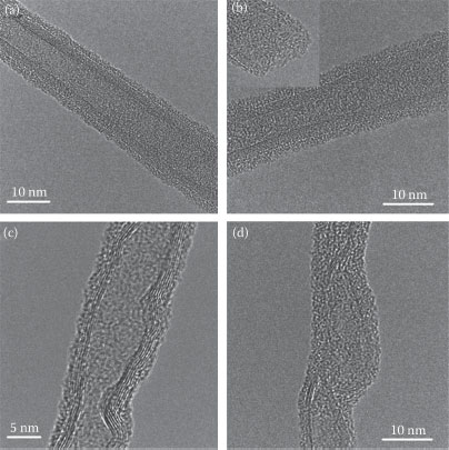
FIGURE 8.1 TEM micrographs of (a) pristine MWCNT sample and samples irradiated with 30 keV Ga ions at doses of (b) 2 × 10¹³, (c) 2 × 10¹⁴, and (d) 4 × 10¹⁴ ions/cm2. The inset of (b) shows the opened tip of MWCNT. (Reprinted with permission from A. C. Ferrari and J. Robertson, Phys. Rev. B 61, 14095, 2000, Copyright 2011, American Institute of Physics.)
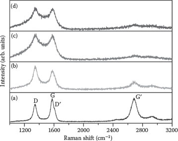
FIGURE 8.2 Raman spectra of (a) pristine MWCNT sample and irradiated samples at doses of (b) 2 × 10¹³, (c) 2 × 10¹⁴, and (d) 4 × 10¹⁴ ions/cm2. The designations are given in the text. (Reprinted with permission from A. C. Ferrari and J. Robertson, Phys. Rev. B61, 14095, 2000, Copyright 2011, American Institute of Physics.)
TABLE 8.1
Summary of Raman Analysis for Pristine and Irradiated Samples
Note: The values shown in parentheses are the full width at half maximum (FWHM) of the corresponding peak.
The upshift in the G-band is caused by stress generated in MWCNTs after Ga+ ion irradiation [25]. The D-band position also shows an upshift, implying that the defects created due to Ga+ ion irradiation have a different energy compared to the as-grown MWCNTs. Third, the presence of a 2D graphene structure in the sample can be monitored by the nature of the G′-band in the Raman spectra [26]. A well-defined G′-band is observable in the case of a pristine sample. As the irradiation dose increases, the intensity of the G′-band decreases and disappears at a dose of 2 × 10¹⁴ ions/cm2. The absence of a D′-band and the decreased intensity of the G′-band indicate the amorphous nature of the samples irradiated at a dose of 2 × 10¹⁴ ions/cm2 and higher.
The electrochemical performance of unirradiated and irradiated samples is shown in Figure 8.3. The double-layer capacitive behavior is clearly observed with near rectangular-shaped voltammograms for all samples. The peak at 0.55 V in the pristine sample can be attributed to oxygen containing functional groups contributing as pseudocapacitance to the overall capacitance. The specific capacitance increases (from 50 to 115 F/g) at 2 × 10¹³ ions/cm2 and then starts decreasing exponentially with increasing irradiation dose and saturates (at 75 F/g) after 2 × 10¹⁴ ions/cm2 as shown in Figure 8.4. The enhanced specific capacitance can be attributed to the defects creation and tip opening of MWCNTs by ion irradiation. The inner cavities of opened-tip nanotubes provide an additional surface to form the EDLC [27]. The HRTEM image shown in the inset of Figure 8.1b confirmed that the inner cavity of the opened-tip MWCNTs can be easily filled with electrolyte. Therefore, the opened-tip nanotubes play a positive role for charging the double layer. HRTEM and Raman results show that after Ga+ ion irradiation, there is an increase of defects in MWCNTs.
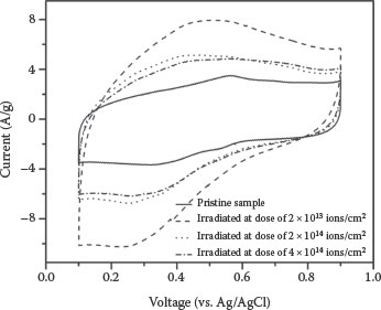
FIGURE 8.3 Cyclic voltammograms recorded at a 50 mV/s for the pristine and Ga ions irradiated MWCNT samples. (Reprinted with permission from A. C. Ferrari and J. Robertson, Phys. Rev. B61, 14095, 2000, Copyright 2011, American Institute of Physics.)
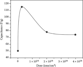
FIGURE 8.4 Variation of specific capacitance of MWCNT samples with ions dose. The specific capacitance decreases with ion dose and shows saturation behavior at higher doses. (Reprinted with permission from A. C. Ferrari and J. Robertson, Phys. Rev. B61, 14095, 2000, Copyright 2011, American Institute of Physics.)
The formation of the defects on the walls of MWCNTs by ion irradiation is very favorable for charging the double-layer capacitance of CNTs, which further improves the capacitive behavior of nanotube electrodes. The defects creation mechanism in MWCNTs can be explained on the basis of electronic and nuclear energy loss in a graphite target by Ga+ ion irradiation.
The electronic and nuclear energy losses of 30 keV Ga+ ion in a carbon target with the density of graphite are estimated to be 0.22 and 1.42 keV/nm, respectively. The dominant mechanism for defect creation on CNTs by irradiation of charged particles is the knock-on atomic displacement due to kinetic energy transfer [28]. The structural transformations in CNTs by irradiation are due to the defects mainly in the form of vacancies and interstitials. For graphitic structures, the threshold energy (Td) required to produce a Frenkel pair is estimated to be 20 eV [28]. Those recoiled atoms with energy slightly above Td can travel more distance in CNTs than in other solids due to the open structure inside the graphitic walls of the CNTs. Controlled defect creation and tip opening of MWCNTs is responsible for peak capacitance obtained at 2 × 10¹³ ions/cm2. The decrease of capacitance at higher doses is attributed to the amorphization of MWCNTs, which lowers the conductivity of nanotubes [29]. The simulation showed that the damage created in the nanotube quickly increases with the irradiation dose. However, at higher irradiation doses, the defect number saturates toward a constant value. This is because at a certain irradiation dose, the system has reached a large degree of disorder so that an incoming energetic ion will not change the internal total coordination numbers substantially.
8.3.2 INTERCALATION OF MOO3–MWCNT NANOCOMPOSITES
Figure 8.5a shows FESEM images of the as-synthesized intertwined MoO3–MWCNT composite. The MWCNTs and MoO3 nanowires in the MoO3–MWCNT composites had mean diameters of ~40 nm and ~50 nm, respectively, with a length in the range of tens of micrometers. The FESEM images showed that the MoO3 nanowires were intertwined in a randomly entangled porous network of MWCNTs. The crystal structure of MoO3 in the composites was examined by TEM. Figure 8.5b presents the TEM images with SAED patterns showing clear diffraction spots in the insets. This pattern is typical for a single crystalline system and the lattice spacing (2.4 Å) is in good agreement with the orthorhombic MoO3. Figure 8.5c shows the XRD patterns of the MoO3 nanowires and MoO3–MWCNT composites. All XRD peaks can be indexed to the orthorhombic structure of the MoO3 phase (JCPDS card no. 05–0508) and crystalline MWCNT phase. As also indicated by electron diffraction, the XRD pattern also showed sharp and well-defined peaks for the MoO3 nanowires, indicating good crystallinity with an orthorhombic phase in the space group Pnma (with lattice constants a = 13.85 Å, b = 3.696 Å, and c = 3.966 Å). The slight decrease (0.08 nm) in the d value for the MoO3–MWCNT composites suggests a decrease in the lattice volume that forms an interconnected network.
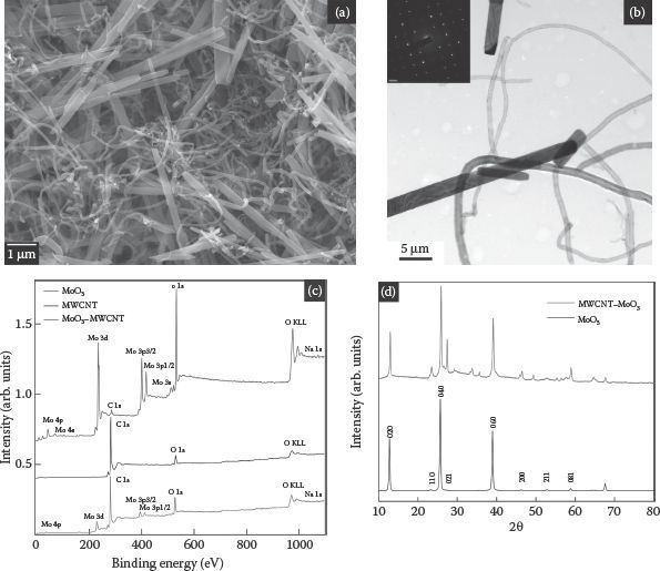
FIGURE 8.5 FESEM image of the MoO3–MWCNT composite synthesized at 180°C for 6 h, (b) HRTEM images MoO3–MWCNT nanocomposites (inset SAED), (c) XPS survey spectrum of MoO3 (top), MWCNT (middle) and MoO3–MWCNT nanocomposite (bottom), and (d) XRD patterns of the α-MoO3 nanowires (bottom) and MoO3–MWCNT composite (top) synthesized at 180°C for 6 h; the MoO3 nanowires show an orthorhombic crystal structure.
The detail of the chemical composition of the composite was measured by XPS. Figure 8.5d shows the XP spectra of molybdenum, oxygen, and carbon of MoO3, MWCNTs, and MoO3–MWCNT nanocomposite. The main peak at 284.6 eV in the MWCNT spectrum was attributed to sp2-hybridized carbon in the graphitic layers of the MWCNTs [30, 31, 32 and 33] and the peak at approximately 285.7 eV was attributed to surface hydroxyl groups [34, 35, 36 and 37]. On the other hand, this C 1s region in the spectrum of the MoO3–MWCNT composite could be deconvoluted into three peaks. The graphite-like carbon peak was found shifted to a higher binding energy due to the formation of Mo–C bonds [38] and the peaks at approximately 286.8 and 288.7 eV were assigned to the C–N and C = O groups, respectively. The Mo 3d5/2 peak positions in the composite are shifted toward a higher binding energy compared to that in MoO3, suggesting the formation of some Mo–C bonds [35, 36 and 38]. Overall, XPS data suggest that MWCNTs and MoO3 in the composite interact via surface oxygen functionality and via some Mo–C bonding. The estimated Mo/carbon ratio was 1:2, which is in agreement with the starting stoichiometry.
The charge storage properties of the MoO3 and MoO3–MWCNT composites were measured by CV in 1 M NaOH and 1 M H2SO4 as shown in Figure 8.6. The charge storage in the layered structure of MoO3 nanowires occurred through the following steps: reaction of cations with an electroactive material followed by a redox reaction, electrochemical adsorption of cations on the electroactive material through a charge transfer process, and the intercalation of ions into the van der Waals gaps of the layered structure of MoO3 [11,39]. In addition to these mechanisms, the presence of the MWCNT matrix serves as an electrical conducting pathway leading to the active sites of MoO3, which contributes to the total capacitance through an electrostatic charge. The enhancement in the capacitance of MoO3 when intertwined with MWCNTs is clearly evident by the increase in current. The inset in Figure 8.6a shows the typical response of the MoO3 nanowires where the electrolyte cation cannot fully utilize the active surface area because of its poor conductivity.
The cathodic half-cycle constitutes the adsorption of the hydrogen ion, while proton desorption occurs in the reverse cycle. The hydrogen ion forms a double layer along the interface and also diffuses into the crystal lattice of MoO3, causing intercalation. As can be seen from Figure 8.6b and d, the cyclic voltammograms show sharp peaks for the first few initial cycles exhibiting the redox behavior of the system. After continuous cycling, there is a smooth electron transition, which can be seen from the diminishing peaks of the voltammograms. Hydrogen evolution is accompanied by the decrease in the capacitance values. The changes in the acid concentration not only enhance the accumulation of charges but also introduce hydrogen evolution at less negative potentials.
The cycle-dependent electrochemical responses of the nanocomposite were examined to better understand the contribution from double-layer and pseudocapacitance. Figure 8.6b and c shows the cyclic voltammograms of an MoO3–MWCNT composite recorded after 5, 10, 50, and 100 cycles at 20 mV/s scan rates. The charge stored in the composite electrode was calculated by integrating the voltammetry current according to the following equation:
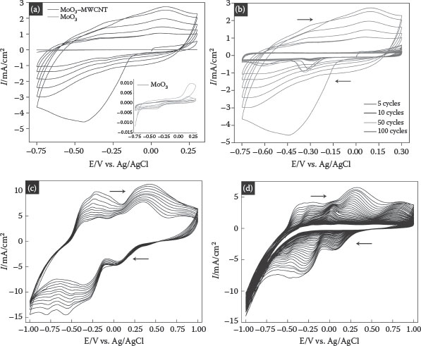
FIGURE 8.6 (a) Cyclic voltammograms of the MoO3–MWCNT nanocomposite and MoO3 nanowires (inset) in 1 M NaOH at 20 mV/s vs. Ag/AgCl as a reference electrode, first five cycles, (b) cyclic behavior of the MoO3–MWCNT nanocomposite in 1 M NaOH at 20 mV/s vs. Ag/AgCl as a reference electrode, (c) cyclic voltammograms of the MoO3–MWCNT nanocomposites in 1 M H2SO4 at 20 mV/s vs. Ag/AgCl as a reference electrode, first 5 cycles, and (d) cyclic behavior of the MoO3–MWCNT nanocomposites in 1 M H2SO4 at 20 mV/s vs. Ag/AgCl as a reference electrode.
(8.1) |
where E is the electrode potential, i is the measured current density, v is the scan rate, and Ec and Ea are the cathodic and anodic potential limits, respectively. Figure 8.7a and b shows the specific capacitance with respect to the cycle number. The initial capacitance was 210 F/g, 178 F/g, which decreased rapidly, leveling off at 110 F/g, 98 F/g after approximately 100 cycles for 1 M H2SO4 and NaOH, respectively. The magnitude of the stored charge for the initial cycles is quite large as the cations can access the active sites of MoO3 through the conducting MWCNT matrix to form an adsorption layer through a charge-transfer process, resulting in redox pseudocapacitance.
The MoO3 nanowires have a highly crystalline layered structure and the MWCNTs provide facile conducting pathways for the cations to enter into the van der Waals gaps (as mentioned earlier), giving rise to an intercalation pseudocapacitance mechanism. The contribution from double-layer capacitance was minor as indicated by the charge-storage magnitude that was strongly dependent on the scan rate.
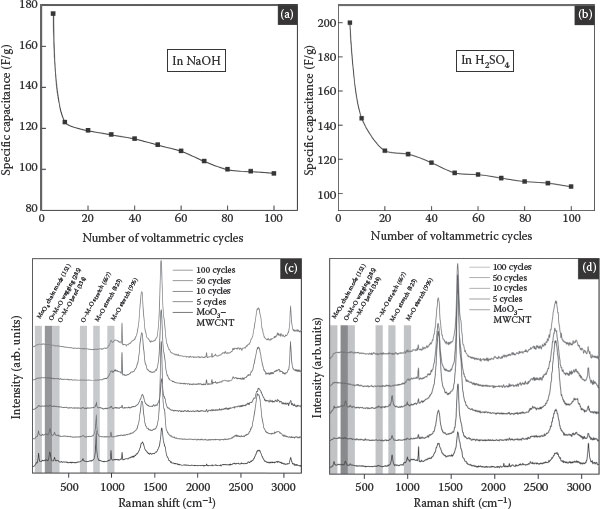
FIGURE 8.7 (a) Specific capacitance decreases upon cycling in 1 M NaOH vs. Ag/AgCl as a reference electrode, (b) specific capacitance decreases upon cycling in 1 M H2SO4 vs. Ag/AgCl as a reference electrode, (c) Raman spectra of MoO3–MWCNTs recorded at 514-nm excitation after 5, 10, 50, and 100 (top) voltammetric cycles in 1 M NaOH vs. Ag/AgCl as a reference electrode, and (d) Raman spectra of MoO3–MWCNTs recorded at 514-nm excitation after 5, 10, 50, and 100 (top) voltammetric cycles in 1 M H2SO4 vs. Ag/AgCl as a reference electrode.
The cycling-induced structural and morphological changes were measured by Raman spectroscopy. Figure 8.7c and d shows the Raman spectra of the MoO3–MWCNT composites before and after cycling (which appear as superpositions of the MWCNT and MoO3 peaks). The Raman peaks observed for MoO3 in the pristine MoO3–MWCNT composite are characteristic of a single-crystal α-MoO3 system, which is a thermodynamically stable phase with a layered structure. Raman bands at 996 (Ag, υs M = O stretch), 823 (Ag, υs M = O stretch), 667 (B2g, B3g υs O–M–O stretch), 473 (Ag, υs O–M–O stretch and bend), 380 (B1g, δ O–M–O scissor), 376 (B1g), 366 (A1g, δ O–M–O scissor), 334 (Ag, B1g, δ O–M–O bend), 293 (B3g, δ O = M = O wagging), 285 (B2g, δ O = M = O wagging), 247 (B3g, τ O = Mo = O twist), 216 (Ag, rotational rigid MoO4 chain mode, Rc), 197 (B2g, τ O = Mo = O twist), 159 (Ag/B1g, translational rigid MoO4 chain mode, Tb), 129 (B3g, translational rigid MoO4 chain mode, Tc), 116 (B2g, translational rigid MoO4 chain mode, Tc), 100 (B2g, translational rigid MoO4 chain mode, Ta), and 89 cm−1 (Ag, translational rigid MoO4 chain mode, Ta) closely resemble the single-crystal bands for α-MoO3, a thermodynamically stable phase with layered structure. There was no β-MoO3 phase present in the sample as the peak at 902 cm−1 was absent.
The Raman spectra of the nanocomposites recorded after five voltammetric cycles in 1 M NaOH and H2SO4 show the structural distortions introduced by the intercalation of Na and H ions decreases, indicating the loss of structural disorder. When Na and H and electrons are inserted into α-MoO3 nanowires, the electrons reduce Mo6+ ions to Mo5+, thus creating Mo5+ = O and Mo5+–O bonds. The intercalation of Na and H ions induces the Mo5+ states by reducing the Mo6+ states. The intensity of the Raman bands of MoO3 in the MoO3–MWCNT composite decreased after five voltammetric cycles, and almost disappeared after 50 cycles, indicating a gradual loss of crystallinity of the MoO3 nanowires, which is most likely due to some degree of irreversible intercalation, as shown in Figure 8.8. This loss of the Raman signature of the α-MoO3 phase was accompanied by a decrease in the charge storage capacity measured by CV. The Raman signature of α-MoO3 disappeared completely after 50 and 100 cycles, which is the region where the specific capacitance becomes constant (Figure 8.8a and b). On the other hand, the Raman spectra also show the structural changes in MWCNTs upon cycling as shown in Figure 8.7c and d. Three distinct peaks can be seen from the spectra: (1) the D-band in the range of 1300–1400 cm−1, which is the disorder-induced band in the graphite lattice that reflects defects in CNTs; (2) the G-band close to 1600 cm−1, which is due to the tangential vibration of carbon atoms; and (3) the D*-band in the range of 2600–2800 cm−1, which is the second harmonic of the D-band. The structural integrity of the nanotubes can be estimated qualitatively by calculating the peak intensity ratio of the D- and G-bands (ID/IG). Figure 8.8c and d shows the ID/IG ratios of the MWCNTs in the composite, which were calculated after 5, 10, 50, and 100 voltammetric cycles.
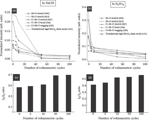
FIGURE 8.8 Decrease of the MoO3 Raman bands in the MoO3–MWCNT nanocomposite upon cycling, indicating structural changes. The peak positions were calculated after fitting with the Lorentzian function and intensities were normalized with respect to the MWCNT G-band (a) 1 M NaOH, (b) 1 M H2SO4. Increase of the ID/IG ratio for MWCNTs with the number of cycles, indicating the structural changes (c) 1 M NaOH and (d) 1 M H2SO4.
The observed gradual increase in the ID/IG ratio is consistent with the increase in defect density in the MWCNT walls, which may result from charge centers appearing on the MWCNTs as a result of faradaic reactions and/or intercalation of the electrolyte into the MWCNT structure. Thus, the MWCNTs act not only as a support matrix that provides electrical conducting pathways to the active sites of the metal oxide but also they contribute to the overall capacitance of the system through faradaic and/or intercalation mechanisms (as well as double-layer formation). The nanocomposite was examined by HRTEM to further visualize the structural and morphological changes. Figure 8.5 shows the HRTEM images and electron diffraction pattern of the MoO3–MWCNT composite after 10 and 100 cycles in 1 M H2SO4 and NaOH. The crystallinity of the MoO3 nanowires changed with increasing cycles, and the diffraction pattern exhibited amorphous rings rather than sharp diffraction spots (Figure 8.5b). This supports the idea that the MoO3 crystal structure is modified irreversibly upon cycling, which is most likely through irreversible cation intercalation.
Electrochemical impedance analysis was performed to gain an understanding of the double-layer and pseudocapacitance of the composite system. Figure 8.6 shows the impedance spectra of the MoO3–MWCNT nanocomposites recorded after 10, 50, and 100 voltammetry cycles in 1 M NaOH and 1 M H2SO4. The impedance plot revealed Rs values (solution resistance or initial resistance) of 0.028 Ω (after 10 cycles), 0.022 Ω (after 50 cycles), and 0.025 Ω (after 100 cycles) in 1 M NaOH and 0.046 Ω (after 10 cycles), 0.048 Ω (after 50 cycles), and 0.039 Ω (after 100 cycles) in 1 M H2SO4.
This shows that the low equivalent series resistance is relatively independent of cycling due to the good electrical conductivity of the MWCNT support network. Initially, redox processes were dominant, resulting in the larger semicircle at higher frequencies. At lower frequencies, diffusion behavior was dominant. The insertion of hydrogen and sodium ions into the interiors of composite materials results in the loss of crystallinity of oxide material and introduces defects on the sidewalls of CNTs. The plots can be further divided into two regions for further analysis: a higher-frequency region that shows the total resistance of the system, and a lower-frequency region dominated by the diffusion behavior. The impedance plots after 10 and 50 cycles show the lower-frequency regions dominated by diffusion phenomena. On the other hand, the impedance plot after 100 cycles shows linearity, which is almost parallel to the imaginary axis, indicating steady capacitive behavior with little diffusion limitation. The decrease in the diffusion with increased cycle number suggested a loss of a slow, diffusion-controlled charge storage process. This can be interpreted as a decrease in the storage mechanism related to intercalation into MoO3. In an acidic medium, the impedance spectra are dominated by a noncapacitive faradaic reaction, probably hydrogen evolution. With a number of cycles, the material exhibits amorphous behavior and the capacitance contribution is mainly due to the formation of a double layer.
The redox kinetics and cycling behavior of the nanoarchitectures of MoO3–MWCNTs can be modified to produce high capacitance values when supported on a conducting support matrix of MWCNT. The electrochemical charge storage in the MoO3–MWCNT composite involves the contribution from double-layer, faradaic, and intercalation mechanisms. CNTs not only offer mechanical integrity to MoO3 but also provide electrical conducting pathways to its active sites. The initial storage capacity was 178 F/g in an basic medium and 190 F/g in an acidic medium, and decreased rapidly with repeated cycling, reaching a steady value of 98 F/g (basic) and 102 F/g (acidic) after approximately 80 cycles. The loss of the MoO3 structure observed by Raman spectroscopy and TEM, as well as impedance spectroscopy, argues toward gradual loss of the intercalation charge storage mechanism upon repeated cycling due to irreversible intercalation.
The effects of morphological disorder of graphene on electron field emission properties are reported below. Figure 8.9a and b shows the morphological distribution of the planar single-layer graphene (PSLG) that seems to be a continuous layer of graphene. Figure 8.9c and d shows the SEM images at different magnifications of agglomerated single-layer graphene (ASLG).
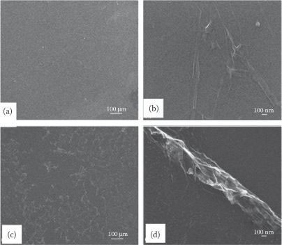
FIGURE 8.9 SEM images of planar (a and b) and aggregated (c and d) graphene at different magnifications. P. Rai et al., Modified carbon nanostructures for energy and display applications, Proc. 11th IEEE International Conference on Nanotechnology, August 15–18, Portland, Oregon, pp. 76–79, © (2011) IEEE. With permission.)
The structural properties and qualities of these two types of samples can be deduced by Raman spectroscopy. Raman spectra of the planar and agglomerated single-layer graphene are shown in Figure 8.10. Both the Raman spectra show the basic feature of a graphene, that is, a G-band that originates from doubly degenerate (iTO and LO) phonon mode (E2g symmetry) at the Brillouin zone center and a 2D band that originates from a second-order process, involving two iTO phonons near the K point [40,41]. The calculated values of the G- to 2D band (IG/I2D) intensity ratio and the D- to G-band (ID/IG) intensity ratio were found to be 0.28 and 0.10, respectively. On the basis of the above data obtained by the Raman spectrometer, we can conclude that our planar graphene shows an excellent agreement with the features of continuous monolayer graphene.
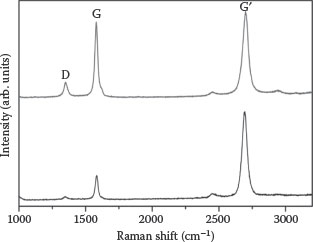
FIGURE 8.10 Raman spectra of planar (lower curve) and agglomerated graphene (upper curve). P. Rai et al., Modified carbon nanostructures for energy and display applications, Proc. 11th IEEE International Conference on Nanotechnology, August 15–18, Portland, Oregon, pp. 76–79, © (2011) IEEE. With permission.)
The upper plot of Figure 8.10 shows the Raman spectrum of the ASLG. The increased value of the ID/IG ratio implies the highly disordered state and increased number of the defects/edges in the agglomerated graphene, and consequently this sample should have more number of sites for field emission. Moreover, after agglomeration of the single-layer graphene, there is a possibility of the formation of the double, triple, or multilayer graphene structure, which this will increase the IG/I2D ratio. Thus, the comparative analysis of the PSLG and ASLG shows that after the agglomeration of monolayer graphene, the emission sites may increase significantly.
Figure 8.11 shows the plot of current density against the applied electric field for PSLG and ASLG, obtained from the field emission characterization technique as described in the experimental section. The turn-on field Eto corresponding to 10 μA/cm2 for the PSLG was found to be 4.31 V/μm, whereas turn-on value Eto corresponding to ASLG was found to be 2.26 V/μm. This enhancement in the field emission properties in ASLG is mainly due to the random shape of the graphene.
If we compare this work with the other graphene-based field emission, we find that pristine ASLG gives similar or better performance without any treatment. For example, Qi et al. [42] reported that the plasma etching treatment for 3 min on the few layers of graphene sheets decreases the turn-on electric field from 3.91 to 2.23 V/μm, and increases the maximum emission current density, drawn at a field of 4.4 V/μm, from 0.033 to 1.330 mA/cm2. But by using our simple method, the turn-on values were found to decrease from 4.31 to 2.26 V/μm and increase in maximum current density from 0.007 to 3.525 mA/cm2 at 4.26 V/μm (Table 8.2 and Figure 8.11). Three very interesting observations can be made from the results obtained. (1) There was considerable reduction in the “turn-on” field for morphologically disordered graphene. (2) βL did not show much difference (%) while the value of βH changed significantly (%). (3) The surface of the planar monolayer graphene has a considerable field enhancement factor.
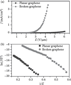
FIGURE 8.11 (a) Plots of the electron-emission current density (J) as a function of applied electric field (E) for the CVD grown planar and broken graphene. (b) Corresponding F–N plots. Nanotechnology (IEEE-NANO), 2011 11th IEEE Conference, pp. 76–79, © (2011) IEEE.)
TABLE 8.2
Different Parameters Obtained from Field Emission Measurements
Sample |
Eturnon (V/μm) |
βL |
βH |
Jm (mA/cm2) |
Planar |
4.31 |
1870 |
2690 |
0.007 |
Agglomerated/broken |
2.26 |
2060 |
3870 |
3.525 |
Source: Nanotechnology (IEEE-NANO), 2011 11th IEEE Conference, pp. 76–79, © (2011) IEEE.
We believe that the reduction in the turn-on field is due to a change in morphology, which gives rise to additional emission sites in the form of defects and irregular nanostructure shapes. Only a slight change in the lower slope of the F–N plot implies the verification of a double barrier model of field emission. Moreover, planar monolayer graphene showed a significant field emission property. We suggest that field emission from planar monolayer graphene come mainly from its grain boundaries. Further investigations are needed to have a better control on the stresses used on the copper foil and then to correlate the extent of morphological disorder to the field emission properties.
In conclusion, we observed that a moderate level of ion irradiation can produce considerable changes in the nanostructures such as MWCNT. Higher doses will result in amorphization, reducing the usefulness of the defect creation. The irradiation levels used in this study are routinely used while carrying out ion etching, and therefore one has to be cognizant of these limitations as well. The electrochemical charge storage in the MoO3–MWCNT composite involves the contribution from double-layer, faradaic, and intercalation mechanisms. The loss of charge storage capacity upon repeated cycling can be explained as due to irreversible intercalation of the nanocomposite. Minute mechanical stresses present while transferring single-layer graphene resulted in improved field emission characteristics. Controlled modifications of carbon nanostructures such as MWCNT and graphene can be used in applications such as supercapacitors and field emission displays.
The support from the Korean Ministry of Education, Science and Technology under the grant R31-2008-10029 (World Class University Program) is greatly appreciated. Technical assistance from the present and past members of the NMESG (NanoMaterials for Energy Science Group) of Sungkyunkwan University is acknowledged. Collaborative work from group members of “Nanoscale Devices and Materials Physics Laboratory” helped to carry out the metal oxide nanocomposite work.
1. K.M. Kadish and R. S. Ruoff (Eds), Fullerenes: Chemistry, Physics and Technology, John Wiley & Sons Inc., New York, 2000.
2. M. Meyyappan (Ed), Carbon Nanotubes: Science and Applications, CRC Press LLC, Boca Raton, 2005.
3. S. Pati, T. Enoki, and C.N.R. Rao (Eds), Graphene and Its Fascinating Attributes, World Scientific Publishing Co Pvt. Ltd., Singapore, 2011.
4. J.R. Miller and P. Simon, Electrochemical capacitors for energy management, Science, 321, 651, 2008.
5. T. Brezesinski, J. Wang, S. H. Tolbert, and B. Dunn, Ordered mesoporous α-MoO3 with iso-oriented nanocrystalline walls for thin-film pseudocapacitors, Nat. Materials, 9, 146, 2010.
6. V.L. Pushparaj, M. M. Shaijumon, A. Kumar, S. Murugesan, L. Ci, Robert Vajtai, R. J. Linhardt, O. Nalamasu, and P. M. Ajayan, Flexible energy storage devices based on nanocomposite paper, Proc.Nat.l Acad.Sci., 104, 13574, 2007.
7. P. Simon and Y. Gogotsi, Materials for electrochemical capacitors, Nature Materials, 7, 845, 2008.
8. Z.W. Pan, Z. R. Dai, and Z. L. Wang, Nanobelts of semiconducting oxides, Science, 291, 1947, 2001.
9. Y. Zhu, Y. Bando, L. Yin, and D. Golberg, Field nanoemitters: Ultrathin BN nanosheets protruding from Si3N4 nanowires, Nano Lett. 6, 2982, 2006.
10. M. Hoefer and P. R. Bandaru, Determination and enhancement of the capacitance contributions in carbon nanotube based electrode systems, Appl. Phys. Lett. 95, 183108, 2009.
11. T. Brezesinski, J. Wang, S.H. Tolbert, and B. Dunn, Ordered mesoporous α-MoO3 with iso-oriented nanocrystalline walls for thin-film pseudocapacitors, Nat. Mater. 9, 146, 2010.
12. H.Y. Lee and J.B. Goodenough, Ideal supercapacitor behavior of amorphous V2O5.nH2O in potassium chloride (KCl) aqueous solution, J. Solid State Chem. 148, 81–84, 1999.
13. A.S. Aricò, P. Bruce, B. Scrosati, J.M. Tarascon, and W. Van Schalkwijk, Nanostructured materials for advanced energy conversion and storage devices, Nat. Mater. 4 366–377, 2005.
14. P. Simon and Y. Gogotsi, Materials for electrochemical capacitors, Nat. Mater. 7, 845, 2008.
15. J. Wang, J. Polleux, J. Lim, and B. Dunn, Pseudocapacitive Contributions to Electrochemical Energy Storage in TiO2 (Anatase) Nanoparticles, J. Phys. Chem. C. 111, 14925, 2007.
16. Z.-S. Wu, S. Pei, W. Ren, D. Tang, L. Gao, B. Liu, F. Li, C. Liu, and H.-M. Cheng, Field emission of single-layer graphene films prepared by electrophoretic deposition, Adv. Mater. 21, 1756, 2009.
17. M. Qian, T. Feng, H. Ding, L. Lin, H. Li, Y. Chen, and Z. Sun, Electron field emission from screen-printed graphene films, Nanotechnology 20, 425702, 2009.
18. A. Malesevic, R. Kemps, A. Vanhulsel, M. P. Chowdhury, A. Volodin, and C. V. Haesendonck, Field emission from vertically aligned few-layer graphene, J. Appl. Phys. 104, 084301, 2008.
19. J.L. Qi, X. Wang, W. T. Zheng, H. W. Tian, C. Q. Hu, and Y. S. Peng, Ar plasma treatment on few layer graphene sheets for enhancing their field emission properties, J. Phys. D: Appl. Phys. 43, 055302, 2010.
20. U.A. Palnitkar, Ranjit V. Kashid, Mahendra A. More, Dilip S. Joag, L. S. Panchakarla, and C. N. R. Rao, Remarkably low turn-on field emission in undoped, nitrogen-doped, and boron-doped grapheme, Appl. Phys. Lett. 97, 063102, 2010.
21. S.R. Sivakkumar, J.M. Ko, D.Y. Kim, B.C. Kim, and G.G. Wallace, Performance evaluation of CNT/polypyrrole/MnO2 composite electrodes for electrochemical capacitors, Electrochimica Acta 52, 7377, 2007.
22. M. Jayalakshmi, M.M. Rao, N. Venugopal, and K.B. Kim, Hydrothermal synthesis of SnO2–V2O5 mixed oxide and electrochemical screening of carbon nano-tubes (CNT), V2O5, V2O5–CNT, and SnO2–V2O5–CNT electrodes for supercapacitor applications, J. Power Sources 166, 578, 2007.
23. F. Gunes, H.-J. Shin, C. Biswas, G. H. Han, E. S. Kim, S. J. Chae, J.-Y. Choi, and Y. H. Lee, Layer-by-layer doping of few-layer graphene film, ACS Nano 4, 4595, 2010.
24. A.C. Ferrari and J. Robertson, Interpretation of Raman spectra of disordered and amorphous carbon, Phys. Rev. B 61, 14095, 2000.
25. A. Misra, P. K. Tyagi, P. Rai, D. R. Mahopatra, J. Ghatak, P. V. Satyam, D. K. Avasthi, and D. S. Misra, Axial buckling and compressive behavior of nickel-encapsulated multiwalled carbon nanotubes, Phys Rev. B 76, 014108, 2007.
26. A.R. Adhikari, M. Huang, H. Bakhru, R. Vajtai, C. Y. Ryu, and P. M. Ajayan, Stability of ion implanted single-walled carbon nanotubes: Thermogravimetric and Raman analysis, J. Appl. Phys. 100, 64315, 2006.
27. Y. Yamada, O. Kimizuka, K. Machida, S. Suematsu, K. Tamamitsu, S. Saeki, Y. Yamada et al., Hole Opening of Carbon Nanotubes and Their Capacitor Performance, Energy Fuels 24, 3373, 2010.
28. A.V. Krasheninnikov and K. Nordlund, Irradiation effects in carbon nanotubes, Nucl. Instr. and Meth. B 216, 355, 2004.
29. Y. Yamada, O. Kimizuka, O. Tanaike, K. Machida, S. Suematsu, K. Tamamitsu, S. Saeki, Y. Yamada, and H. Hatori, Capacitor properties and pore structure of single- and double-walled carbon nanotubes, Electrochemical and Solid-State Letters 12, K14, 2009.
30. P. Li, X. Lim, Y. Zhu, T. Yu, C.K. Ong, Z. Shen, A.T.S. Wee, and C.H. Sow, Tailoring wettability change on aligned and patterned carbon nanotube films for selective assembly, J. Phys. Chem. B 111, 1672, 2007.
31. N.I. Kovtyukhova, T.E. Mallouk, L. Pan, and E.C. Dickey, Individual single walled nanotubes and hydrogels made by oxidative exfoliation of carbon nanotube ropes, J. Am. Chem. Soc. 125, 9761, 2003.
32. D. Yu and L. Dai, Self-Assembled graphene/carbon nanotube hybrid films for supercapacitor, J. Phys. Chem. Lett. 1, 467, 2010.
33. C.H. Chen, H. C. Su, S. C. Chuang, S. J. Yen, Y. C. Chen, Y. T. Lee, H. Chen et al., Hydrophilic modification of neural microelectrode arrays based on multi-walled carbon nanotubes, Nanotechnology 21, 485501, 2010.
34. C.C. Lin, B.T.T. Chu, G. Tobias, S. Sahakalkan, S. Roth, M.L.H. Green, and S.Y. Chen, Electron transport behavior of individual zinc oxide coated single-walled carbon nanotubes, Nanotechnology 20, 105703, 2009.
35. T. Wei, G. Luo, Z. Fan, C. Zheng, J. Yan, C. Yao, W. Li, and C. Zhang, Preparation of graphene nanosheet/polymer composites using in situ reduction–extractive dispersion, Carbon 47, 2296, 2009.
36. S. Stankovich, D.A. Dikin, R.D. Piner, K.A. Kohlhaas, A. Kleinhammes, Y. Jia, Y. Wu, S.T. Nguyen, and R.S. Ruoff, Synthesis of graphene-based nanosheets via chemical reduction of exfoliated graphite oxide, Carbon 45, 1558, 2007.
37. S. Park, J. An, R.D. Piner, I. Jung, D. Yang, A. Velamakanni, S.T. Nguyen, and R.S. Ruoff, Aqueous suspension and characterization of chemically modified graphene sheets, Chem. Mater. 20, 6592, 2008.
38. L. Fu, Z. Liu, Y. Liu, B. Han, P. Hu, L. Cao, and D. Zhu, Beaded cobalt oxide nanoparticles along carbon nanotubes: Towards more highly integrated electronic devices, Adv. Mater. 17, 217, 2005.
39. I. Shakir, M. Shahid, H.W. Yang, and D.J. Kang, Structural and electrochemical characterization of α-MoO3 nanorod-based electrochemical energy storage devices, Electrochim Acta 56, 376, 2010.
40. L.M. Malard, M.A. Pimenta, G. Dresselhaus, and M.S. Dresselhaus, Raman spectroscopy in graphene, Physics Reports, 473, 51, 2009.
41. A. Reina, X. Jia, J. Ho, D. Nezich, H. Son, V. Bulovic, M. S. Dresselhaus, and J. Kong, Large area, few-layer graphene films on arbitrary substrates by chemical vapor deposition, Nano Lett. 9, 30, 2009.
42. J.L. Qi, X. Wang, W. T. Zheng, H. W. Tian, C. Q. Hu, and Y. S. Peng, Ar plasma treatment on few layer graphene sheets for enhancing their field emission properties, J. Phys. D: Appl. Phys. 43, 055302–08, 2010.
43. P. Rai, S. Pandey, G. Arabale, P. Nikolaev, and S. Arepalli, Modified carbon nano structures for energy and display applications, Proc. 11th IEEE International Conference on Nanotechnology, August 15–18, Portland, Oregon, pp. 76–79, 2011.