
CONTENTS
12.2 Nanoscale Devices and Circuit Applications
12.2.1 Conventional Devices and Circuits
12.2.2 Nonconventional Devices and Circuits
12.3 Ballistic Deflection Transistors
12.4 Logic Design with Ballistic Deflection Transistors
12.4.2 Two-Input NAND Gate with BDTs
12.4.3 General-Purpose Gate with BDTs
12.5 Circuit Design with Ballistic Deflection Transistors
12.5.1 BDT Circuit Design Methodology
12.5.2 Case Study: BDT Full Adder
12.6 Limitations and Potential Solutions
12.6.2 Alternative BDT Connection Methods
12.6.3 Future Circuit Improvements
As complementary metal-oxide-semiconductor (CMOS) transistors near atomic-scale limitations, researchers are searching for novel devices to complement or supplant conventional silicon electronics. Several alternative devices have been proposed as potential successors to conventional Si CMOS. Unlike the transition from bipolar devices to CMOS, however, a clear successor to the metal-oxide-semiconductor field-effect transistor (MOSFET) has not yet emerged. Some devices offer improved speed, some promise unmatched power efficiency, and still others offer versatility and robustness through runtime configurability. Because no device is superior in every metric, future computing systems may offer heterogeneous integration of CMOS and other technologies, providing a judicious balance among the devices optimized for the particular performance metric desired.
This chapter describes a recent entrant into the emerging devices landscape, the ballistic deflection transistor (BDT) [1], which promises terahertz speeds. In Section 12.2, we provide a brief overview of nanoscale devices and their circuit applications. Section 12.3 describes the operation of the BDT, including ballistic transport in two-dimensional electron gas (2DEG) heterostructures. In Section 12.4, we present examples of BDT logic gates—an inverter, a two-input NAND, and a two-input general-purpose gate (GPG) used to construct random logic. BDT circuit design methodology, a full adder implementation case study, and a discussion of applications suited for BDTs are presented in Section 12.5. Future work on voltage-mode BDT logic and potential limitations are discussed in Section 12.6, and conclusions are presented in Section 12.7.
12.2 NANOSCALE DEVICES AND CIRCUIT APPLICATIONS
12.2.1 CONVENTIONAL DEVICES AND CIRCUITS
Conventional device improvements include new material structures, fabrication processes, or integration methods that have properties similar to standard MOSFETs. Surveys of nanoscale devices emphasizing these traditional improvements are available, for example, Refs. [2,3]. For the continued scaling of conventional MOSFETs beyond the 14 nm node, new lithography techniques such as extreme ultraviolet lithography, double patterning, and immersion lithography are being explored [4]. III–V compound semiconductors, such as GaAs, have been used in electronic and optical applications, resulting in operating frequencies of over 250 GHz in a GaAs heterojunction bipolar transistor (HBT) [5]. Channel properties can be adjusted through the use of Ge, SiGe, or strained Si approaches [6]. An excellent discussion of these techniques is available in Ref. [7], with mobility improvements of up to 10× reported. Metal gates with high-κ dielectrics, multigate FETs [8], and finFETs [9] have been employed to reduce leakage current and improve Ion/Ioff ratios. Silicon-on-insulator (SoI) technology enables large performance improvements and a tighter control of noise, coupling, and substrate leakage [2]. Ultrathin SoI substrates have facilitated the creation of 3D integrated circuits [10], which reduce the wire length, improve the latency and system performance, and enable the integration of different substrates [11]. As device dimensions reach the electron mean free path at room temperature in some materials, ballistic transport can be harnessed, promising terahertz-range frequencies [12, 13 and 14] (ballistic devices will be discussed in more detail in Section 12.3).
12.2.2 NONCONVENTIONAL DEVICES AND CIRCUITS
Nonconventional devices exhibit properties fundamentally different from conventional CMOS. Molecular structures have been used to create both passive and active devices [15,16]. For example, nanowires can be used with active molecular switches to create logic crossbar structures, such as memristor crossbar latches [17]; nanowires are also finding use as gate channels [18]. Graphene sheets, nanoribbons, and carbon nanotubes can exhibit either metallic or semiconducting properties depending on their chirality; these structures have some of the highest carrier mobilities of any known device, and should enable operating frequencies well into the terahertz range [19,20]. In addition, nanotube devices can utilize band-to-band tunneling to achieve very low power consumption [21,22]. These features have encouraged a great deal of research on nanotube circuit modeling [23] and implementations such as frequency doublers and mixers [20]. Single-electron transistors (SETs) [24,25] are deep nanoscale devices that make use of the Coulomb barrier tunneling to provide logic. This “one electron at a time” transport can be regarded as the ultimate limit in low-power nanoelectronics. SET logic has been explored using both a traditional voltage-mode operation and a novel charge state logic where the state is determined by whether or not an electron is present in a node [26]. Spintronics [27,28] uses the spin of an electron or a group of electrons to encode logic information, and can be reconfigured at runtime by adjusting the device magnetization. Ferromagnetic semiconductors are increasingly implemented as spin-valve devices [27] and offer promise for large, nonvolatile random-access memories. An excellent survey of nontraditional devices can be found in Ref. [29].
Research is also ongoing in the areas of DNA computing [30,31], peptide computing [32], and, most notably, quantum computing [33]. These technologies promise immense computational power for parallel computing problems such as database searches and large number factorization. Finally, nonlinear optical devices such as semiconductor all-optical switches and amplifiers have recently been used to create Boolean logic functions [34]. These devices will be immensely useful in fiber optic systems, circumventing the bandwidth limitations of electro-opto conversions.
12.3 BALLISTIC DEFLECTION TRANSISTORS
One promising group of devices utilizes ballistic transport, with near-terahertz results already reported [12,13]. Various III–V compound heterostructures, such as AlGaAs/InGaAs or InGaAs/InAlAs systems, can be used to create a 2DEG layer with very high electron mobilities [35]. In 2DEG structures with dimensions smaller than the electron mean free path le, electrons can travel without any scattering events. This is referred to as ballistic transport and can be observed even at room temperature, for example, Refs. [36,37]. One-dimensional electron gas transistor channels have been used to create high-electron-mobility transistors (HEMTs) [38], which can exhibit up to terahertz performance.
Ballistic transport can be explained using Figure 12.1, which is derived from an experiment by Hirayama and Tarucha [39]. The black lines are boundaries, electrons are ejected from terminal 1, and terminal 2 is positively charged. In the ordinary drift-diffusive transport regime, scattering eliminates the initial electron momentum before electrons enter the central region. This loss of momentum is defined by the momentum relaxation time
(12.1) |
where m* is the electron effective mass, μ is the electron mobility, and e is an elementary charge. Scattered electrons drift toward the positively charged terminal 2, resulting in the electron flow shown in Figure 12.1a. As transport becomes more ballistic, τm increases and electrons maintain their momentum for a longer period, resulting in a larger percentage of carriers reaching terminal 3 instead of terminal 2. In the ballistic limit (where τm is much larger than the travel time between terminals 1 and 3), electron paths follow a billiard model [40], and most electrons travel from terminal 1 to terminal 3, shown in Figure 12.1b. In the region between ballistic and drift-diffusive transport, electrons behave quasi-ballistically and can be guided by applied potentials and geometrical boundaries. In semiconducting 2DEG systems, τm and le strongly depend on temperature, so devices that are ballistic at liquid nitrogen or liquid helium temperatures can become drift-diffusive at room temperature. A number of novel devices have been proposed using 2DEG ballistic transport [36,41, 42, 43, 44 and 45]. In this chapter, we focus on the BDT.
The BDT [14] is a six-terminal coplanar structure etched into a 2DEG. The device consists of a grounded electron source, left and right gates, and three biased drains. The center drain is a constant pull-up potential used to accelerate the electrons from the source toward the central deflector; the left and right drains are outputs. The dimensions and materials allow the electrons to travel in a quasiballistic manner at room temperature, guided by the deflector and lateral gate potentials as shown in Figure 12.2. A SEM image of a BDT is shown in Figure 12.3. The steering voltage is much smaller than that required for gate pinch-off (e.g., in the results shown, differential input voltages of ±150 mV are used). The low capacitance of the 2DEG features (~0.2 fF) [36] the results in an estimated fT in the terahertz range. Mateos et al. [12] have shown a 1 THz response in a similar structure, the ballistic rectifier.
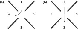
FIGURE 12.1 (a) Drift-diffusive transport versus (b) ballistic transport.
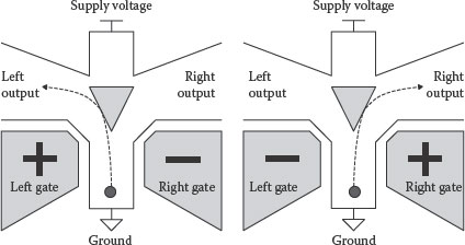
FIGURE 12.2 Schematic of BDT shown under two gate bias conditions.
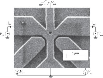
FIGURE 12.3 SEM image of a fabricated BDT.
The BDT has been fabricated in an In0.53Ga0.47As–In0.52A10.48As heterostructure with an InP substrate, using mask layers defined by electron beam lithography, with reactive ion etching used to create the raised mesas shown in the SEM image of Figure 12.3. The 9 mm thick 2DEG occurs about 60 nm beneath the surface. The minimum etch width is 70 nm (the gate–channel spacing) and the etch depth is approximately 130 nm. The electron beam lithography process is less susceptible to orientation changes, diffraction effects, or other photolithography issues; however, in large designs, beam drift can still result in variations. Additional information about the process used is available in Ref. [46]. The electron mean free path in the 2DEG is calculated to be 120 nm [46]; still ballistic effects are observed at room temperature.
The room temperature measured response of the BDT across a range of differential gate voltages is shown in Figure 12.4, with a grounded source and 1 V bias applied to each of the three drains. The x-axis is the left gate voltage. The asymmetry between the left and right outputs is caused by process variation and a slight offset in contact placement. A positive left gate and negative right gate voltage results in current gain through the left output branch; current gain is seen through the right output branch when the voltages are reversed. The overlapping response in Figure 12.4 is a result of electrons scattering away from the intended output.
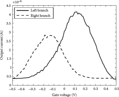
FIGURE 12.4 Measured output response of the BDT.
A major challenge of cascading logic with BDTs is converting the output current of one device into the input voltage of the next device. In the BDT, an accumulated gate charge is not dissipated by switching the driving gate input; instead, the lack of driving current creates a high resistance path to VDD and ground through the driving device. One solution is to use a string of resistors between VDD (e.g., 1 V) and VSS (e.g., −1 V) as a current-to-voltage converter, shown outside the dashed box in Figure 12.5. The output current from the BDT affects the voltage division between VDD and VSS, and the resistor values can be calculated such that the output nodes Vout match the range of input gate voltages (i.e., if Vg,left and Vg,right equal −0.15 and 0.15 V, respectively, Vout,left and Vout,right will equal 0.15 and −0.15 V, respectively). More electrons on a node result in a lower voltage; thus, a flow of electrons represents logic “0.”
The empirical model in Figure 12.5 uses two voltage-controlled current sources (VCCS) to recreate the output behavior from Figure 12.4. The model in Figure 12.5 assumes that the two gate voltages are differential; for nondifferential gate voltages, each VCCS instance must be replaced by a two-input polynomial VCCS (PVCCS) instance, with both gate voltages connected to each PVCCS. The six-terminal behavioral model is completed with a leakage path between ground and the supply voltage, represented by a resistor. To simplify the model, output symmetry is forced by inverting the measured right channel response of about 0 V to create the left channel response.
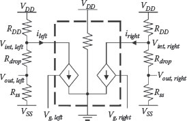
FIGURE 12.5 Empirical model of the BDT.
The BDT has been successfully tested at 20 GHz (the maximum operating frequency of the available equipment); however, the low capacitance of the 2DEG gate structures should yield operating frequencies in the terahertz range. Future experiments include designing a terahertz-capable test environment to determine the maximum operating frequency.
There are four sets of current paths in the BDT that consume power—(1) a path between the top drain and the source (~0.8 μA over a 1 V drop), (2) a path between VDD and VSS in the current-to-voltage converter (two ~2 μA paths over a 2 V drop), (3) a path between VDD in the current-to-voltage converter and the BDT source (the total current through both output drains is 4.6 μA over a 1 V drop), and (4) the average gate leakage current (two gates with leakage 0.4 μA over an average 1 V drop). This results in a net power consumption of 14.2 μW and does not include the switching of the ~2 fF gate capacitance, which is likely to be very small compared to the static currents. In contrast, a 0.5 μm NMOSFET from a commercial 65 nm technology consumes an average of 174 μW. In addition, a single BDT provides the same functionality as a dual-rail CMOS inverter, providing more functionality for lower equivalent power consumption.
12.4 LOGIC DESIGN WITH BALLISTIC DEFLECTION TRANSISTORS
In this section, we explore logic gate design with ballistic deflection transistors while providing three different types of results. The first proof of concepts is evaluated using a Monte Carlo particle simulator based on classical mechanics [47], building upon the billiard model proposed by Beenakker and van Houten [40]. Screenshots from this simulator provide an intuitive picture of predicted electron flows through the device. In addition to the Monte Carlo simulator, we have created an empirical model of the BDT based on measurements of a single device. This empirical model is extrapolated to provide a gate-level functional analysis of the designs that includes the various nonidealities of the fabricated devices. Finally, the measurement results of each logic gate are provided to prove the functionality of each presented logic gate.
The BDT provides complementary outputs; thus, a single BDT can act as both an inverter and a buffer. For example, if we examine Figure 12.4, an input of 0.15 V (logic “1”) produces a large current in the left output branch and a small current in the right output branch. A large output current reduces the output voltage of that branch (the resulting output voltage is a function of the output current and the current-to-voltage converter on that output), creating a logic “0”—the inverted input. On the opposite output terminal, the small output current has little effect on the output voltage, maintaining a logic “1”—the same value as the input.
12.4.2 TWO-INPUT NAND GATE WITH BDTS
The two-input NAND gate can be used to construct any arbitrarily complex logic function; thus, achieving this function in novel devices is an important milestone if they are to be used for general-purpose computation. The NAND gate design [48] shown in Figure 12.6 (with the SEM image in Figure 12.7) functions as follows: the source is shown as the arrow entering the bottom channel of the BDT labeled “1.” The differential gate inputs A and Ā guide electrons into the channel labeled A = 1 when gate A is high and gate A is low, and into channel A = 0 in the opposite case. The differential gate inputs B and guide electrons in the central region to the channels labeled B = 0 or B = 1 similar to gate A. This results in a flow of electrons (representing a “0”) at the output F only when both A and B are high. For each other input combination, electrons are diverted to either the left output channel or the top right output channel. This behavior results in the logic function A NAND B.
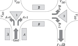
FIGURE 12.6 BDT two-input NAND gate schematic.
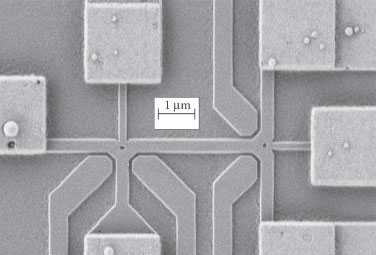
FIGURE 12.7 SEM image of the BDT NAND gate.
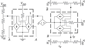
FIGURE 12.8 Circuit model of the BDT NAND gate.
The empirical model in Figure 12.8 is similar to the schematic in Figure 12.6, with a currentcontrolled voltage source (CCVS) allowing the VCCS instances in BDT 2 to react to the current exiting BDT 1. The CCVS has no physical equivalent in the gate, but is needed in the circuit model to convert the output signal from BDT 1 into a voltage to adjust the VCCS in BDT 2.
Here, we describe an important improvement to the model presented in Ref. [48]. In the previous model, it was assumed that the drain potentials in both BDTs were properly balanced, which would result in the A = 0/B = 1 and A = 1/B = 0 states having the same output voltage. Unfortunately, that is not the case, as shown by the measurement results from the fabricated BDT NAND gate in Figure 12.9b. The uneven drain potential increases the amount of incorrectly steered current in BDT 1, such that even when A = 0, a large current flows into BDT 2; when B = 1, that undesired current flow reduces the output voltage (see A = 0/B = 1 in Figure 12.9b), limiting the gate’s Ion/Ioff ratio.
To consider this effect in our empirical model, we have added a new parameter that allows us to tune the switching behavior of BDT 1 by adjusting the current of the A = 0 case (VLow). The adjustment is made by connecting the drains of each device to that device’s VCCS instances, which take the difference between the drain potentials and scale the results according to the empirical data. As shown in Figure 12.9a, adjusting VLow allows us to closely match the reduced A = 0/B = 1 state from the measured results. To tune the model, we performed an additional experiment on a single BDT in which we varied the left output drain bias while keeping the right output drain bias fixed. Based on the empirical data, we found that when the left drain bias is just 33% of the right drain bias (a loose approximation of three biased drains to the right of BDT1 and one biased drain to the left of BDT1), the switching ratio is reduced to just 54% of the ratio when the output drains are equal. VLow =54% correlates very closely with our model in Figure 12.9a, which shows that the A = 0/B = 1 state in the measured results falls within the range of VLow = 40% and VLow = 60%. All transient waveforms in this chapter were taken at low frequency, using an arbitrary clock cycle of 1 ns for simulations and representing DC measurement results in transient format for presentation purposes.
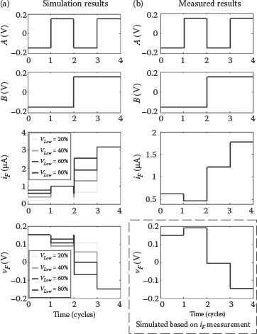
FIGURE 12.9 BDT NAND gate waveforms. (a) Simulated. (b) Measured.
Note that the fabricated gate did not include the current-to-voltage converters; the measured output currents iF in Figure 12.9b are passed through a simulated current-to-voltage converter to provide the voltage response vF in the dashed box. The empirical model is generated from a different chip than the fabricated NAND gate; thus, although the relative behaviors of the model and measurements are very similar, the magnitudes of the output currents are unequal. This is corrected in the voltage outputs by adjusting the current-to-voltage converters.
12.4.3 GENERAL-PURPOSE GATE WITH BDTS
To improve the utility of BDTs in digital logic applications, we have designed a new type of gate structure that is symmetric, reducing the problem of uneven drain potentials that limited the NAND gate response. The design consists of three BDTs [49] with the sources of two rotated BDTs connected to the left and right drains of a center BDT, shown in Figure 12.10 (with the SEM image in Figure 12.11). Electrons are injected through the source, S, and steered to the left or right BDT by gate inputs A and Ā. As the electrons are drawn to the pull-up potentials on either side, gate inputs B and further steer the electrons to one of four output drains.
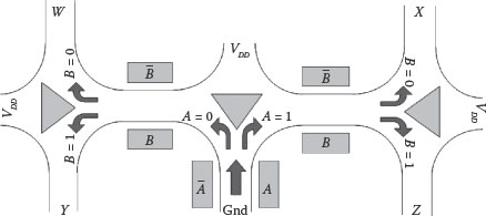
FIGURE 12.10 BDT general-purpose gate (GPG) schematic. D. Wolpert et al., General purpose logic gate using ballistic nanotransistors, Proc. 11th IEEE Conf. Nanotechnol., Portland, OR, p. 1, © (August 2011) IEEE. With permission.)
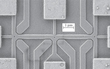
FIGURE 12.11 SEM image of the BDT general-purpose gate (GPG). D. Wolpert et al., General purpose logic gate using ballistic nanotransistors, Proc. 11th IEEE Conf. Nanotechnol., Portland, OR, p. 1, © (August 2011) IEEE. With permission.)
The novelty of this gate structure is that there are four gate outputs, each corresponding to a specific combination of inputs A and B. We label these outputs W, X, Y, and Z, and they correspond to the input values A = B = 0, A = 1 & B = 0, A = 0 & B = 1, and A = B = 1. The logic function of the GPG is defined by how these four drains are connected to output terminals F and , as shown in Table 12.1. This structure is capable of producing any two-input function and its complement; thus, we name the structure as a two-input GPG.
If a drain is connected to terminal F, only one of the four input vectors (e.g., A = B = 0 for drain W) will result in a flow of electrons through that drain, reducing the voltage at F; thus, connecting a drain to output terminal F sets that table entry to logic low, while connecting a drain to output terminal sets that table entry to logic high. For example, the BDT NAND gate shown in Figure 12.8 is very similar to the combination of the center and right BDTs in Figure 12.12. In the NAND gate, the function A NAND B is achieved by connecting the lower right drain to an output F. In the GPG, the function A NAND B is also achieved by connecting the lower right drain (Z) to F. Indeed, the circuit model for the GPG, shown in Figure 12.12, is the same for the center and right-side BDTs as the circuit model for the NAND gate from Figure 12.8; however, the simulation results shown for the GPG in the NAND configuration, discussed momentarily, do not have the same asymmetry issues as the two-BDT NAND gate, resulting in a much larger Ion/Ioff ratio. The improved asymmetric circuit model presented in the previous subsection is not needed for the GPG (aside from process variations) because of the improved device symmetry. A list of output terminal connections for other common logic functions is provided in Table 12.2.
TABLE 12.1
General-Purpose Gate Function
Definition |
||
A |
B |
F |
0 |
0 |
W |
0 |
1 |
Y |
1 |
0 |
X |
1 |
1 |
Z |
If W|X|Y|Z connected to , truth table entry is 1
If W|X|Y|Z connected to F, truth table entry is 0
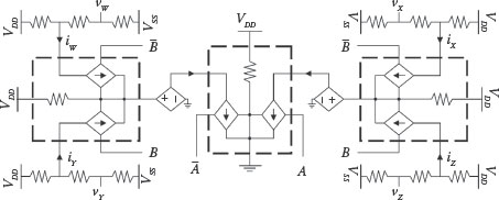
FIGURE 12.12 Circuit model of the BDT general-purpose gate (GPG). D. Wolpert et al., General purpose logic gate using ballistic nanotransistors, Proc. 11th IEEE Conf. Nanotechnol., Portland, OR, p. 2, © (August 2011) IEEE. With permission.)
TABLE 12.2
GPG Connections for Common Logic Functions
|
Terminal Connections |
|||
Function |
W |
X |
Y |
Z |
NAND |
F |
|||
AND |
F |
F |
F |
|
NOR |
F |
F |
F |
|
OR |
F |
|||
XNOR |
F |
F |
||
XOR |
F |
F |
||
In Figure 12.13, we present the measurement results of a fabricated GPG connected in XOR and XNOR configurations. In Figure 12.13b and c, the measured current response iF represents the current flowing out through the terminals connected to F. The measured output currents were passed through simulated current-to-voltage converters to generate the output voltages vF, which could then be applied to successive BDT logic stages. In this chip, input voltages of only ±100 mV are sufficient to switch between logic states, resulting in a noise margin of approximately 7 μA in the XNOR configuration and 5 μA in the XOR configuration. The peak current in the XNOR configuration is 24 μA, resulting in an Ion/Ioff ratio of 1.6. The Ion/Ioff ratio is expected to improve dramatically as the geometries and process steps are further refined. Gate leakage was particularly problematic in the fabricated test chip—the large potential difference between the gate and the 1V drain biases causes a gate leakage of ~20 μA in the fabricated GPG.
In Figure 12.14, we present the XOR and XNOR simulation results corresponding to the measurements in Figure 12.13. The waveforms match very closely with the exception of small asymmetries in the A = 0/B = 1 and A = 1/B = 0 cases resulting from process variations. In Figure 12.15, we present simulation results from the GPG configurations of other common logic functions, demonstrating the versatility of the GPG for circuit design. In each configuration, the current-to-voltage converters need to be modified depending on how many BDT drains are connected to the internal voltage node (VINT from Figure 12.5) of terminals F and . As shown, each output response is capable of closely reproducing the input voltage range, resulting in a straightforward connection to the gate input of the next stage of the GPG or other devices. An additional advantage of the GPG is its potential for use as a device fabric [50]; the slower e-beam processing could be used to print dies full of unconnected GPGs, and a conventional metallization process could be used to add the resistors and connect the gates into the desired functionality. While this could also be done with the NAND gate, the GPG is capable of creating any two-input logic function using only three BDTs, while multiple NAND gates are required to create most functions. For example, to create an XNOR function, five NAND gates are required (corresponding to 10 BDTs), while the GPG can create that functionality by using only three BDTs. Work is currently underway to improve the speed of e-beam processing the using arrays of beams working simultaneously; this method has the added benefit of eliminating the costly process of fabricating nanoscale masks [51].
12.5 CIRCUIT DESIGN WITH BALLISTIC DEFLECTION TRANSISTORS
In this section, we present a circuit design methodology for integrating discrete BDT logic gates into a larger system. First, we examine a logic cell, and then we use this cell in a case study—a full adder design consisting of five GPCs. We also discuss a number of design considerations for BDT circuits using our empirical circuit model, including necessary modifications to the concept of noise margins and constraints when cascading devices. Finally, we describe potential system applications for BDT logic.
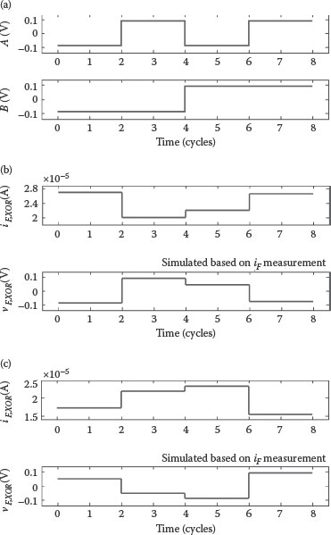
FIGURE 12.13 Measured current response of fabricated GPG. (a) Input voltages, (b) XOR configuration, and (c) XNOR configuration, with simulated current-to-voltage conversion shown for each case. D. Wolpert et al., General purpose logic gate using ballistic nanotransistors, Proc. 11th IEEE Conf. Nanotechnol., Portland, OR, p. 2, © (August 2011) IEEE. With permission.)
12.5.1 BDT CIRCUIT DESIGN METHODOLOGY
Circuit design with BDTs is somewhat similar to the traditional dual-rail logic design; each logic gate requires complementary gate inputs. Unlike the traditional logic design, the outputs F and are generated by connecting the BDT drains to current-to-voltage converters, which then produce the desired output voltage. These additional internal connections complicate circuit design, so we begin with a simple case of one logic cell; in the next subsection, we will show how to combine these logic cells to create more complex functionality.
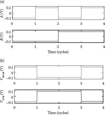
FIGURE 12.14 Simulation results from the BDT general-purpose gate model. (a) Input vectors. (b) GPG XNOR/XOR response. D. Wolpert et al., General purpose logic gate using ballistic nanotransistors, Proc. 11th IEEE Conf. Nanotechnol., Portland, OR, p. 3, © (August 2011) IEEE. With permission.)
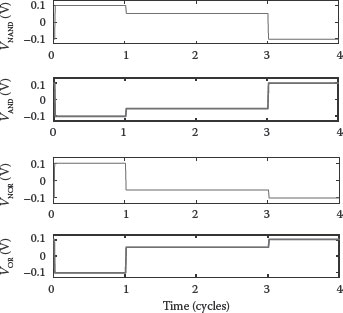
FIGURE 12.15 Simulation results from the other BDT GPG configurations using the inputs in Figure 12.16a. D. Wolpert et al., General purpose logic gate using ballistic nanotransistors, Proc. 11th IEEE Conf. Nanotechnol., Portland, OR, p. 3, © (August 2011) IEEE. With permission.)
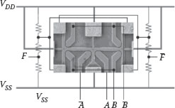
FIGURE 12.16 A BDT XOR/XNOR logic cell. D. Wolpert et al., General purpose logic gate using ballistic nanotransistors, Proc. 11th IEEE Conf. Nanotechnol., Portland, OR, p. 3, © (August 2011). With permission.)
The logic cell consists of a GPG, two current-to-voltage converters, and power and ground rails. The current-to-voltage converters provide the outputs F and , defined by the GPG output drain connections as shown in Table 12.2. An example of an XOR/XNOR logic cell is shown in Figure 12.16. The voltage rail connections and current-to-voltage converters are indicated by the lighter-colored lines. Inputs A and Ā are connected to the central BDT, while inputs B and are connected to both the left and right BDTs. The GPG outputs are connected such that the left current-to-voltage converter provides F = A XOR B, while the right current-to-voltage converter provides .
Defining multicell circuit functionality (an example of a multicell circuit is provided in Figure 12.17a) is a three-step process. First, we create a grid of “unconfigured” logic cells (meaning the GPG inputs and outputs of each cell are left floating), one cell per logic gate in the circuit. Then we analyze the circuit and group any interconnected gates together to attempt to minimize interconnect distances. Once we have found an appropriate logic gate mapping, we define each GPG by connecting the appropriate output drains to the current-to-voltage converters in that cell with metal wires. Finally, we connect the logic cells by connecting each output F and F to the appropriate inputs in the following cell using metal wires.
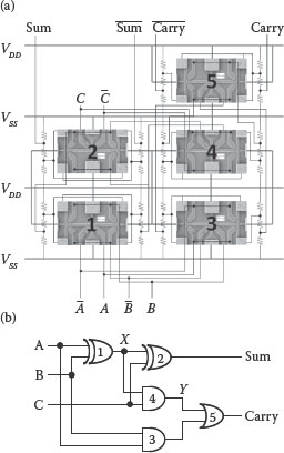
FIGURE 12.17 BDT full adder. (a) GPG-based design and (b) corresponding gate schematic. D. Wolpert et al., General purpose logic gate using ballistic nanotransistors Proc. 11th IEEE Conf. Nanotechnol., Portland, OR, p. 4, © (August 2011). With permission.)
During this connection process, we can also pay attention to the output load of each cell. As shown in Figure 12.16, input A is only connected to a single gate, while input B is connected to two gates. To balance the load when connecting up multiple logic cells, cells that drive multiple other cells should be routed first so that they can be connected to the single input (A) whenever possible, rather than the double input load (B).
12.5.2 CASE STUDY: BDT FULL ADDER
The use of the GPG logic cells makes a circuit layout very regular (aside from signal routing), as shown in Figure 12.17a for a 5-GPG full adder. In Figure 12.17a, the voltage rail connections and current-to-voltage converters are indicated by the lighter-colored lines, which form a simple grid pattern. The gate schematic in Figure 12.17b is provided to make the logic connections in Figure 12.17a easier to follow. Note that GPG 2 and GPG 4 are inverted to simplify connection with the power and ground rails.
The output waveforms in Figure 12.18 indicate that the circuit functions correctly, although the voltage difference between logic high and logic low in the carry input is reduced. To explore why the sum behavior is in full swing and the carry behavior is not, we have included waveforms for the nodes labeled X and Y in Figure 12.17b. Node X corresponds to the output A XOR B. Following the probability analysis presented in Ref. [48] and the simulation results in Figure 12.14, we see that the A = 1/B = 0 and A = 0/B = 1 input states in the XOR gate outputs are in full swing; thus, the output remains a full swing after passing through the XOR-configured GPG. The full-swing output of GPG 1 also enables a full-swing output in GPG 2, resulting in the desirable Sum waveform shown in Figure 12.18. Unfortunately, the carry generation circuit requires AND and OR GPG configurations, which do have reduced-swing states for the A = 1/B = 0 and A = 0/B = 1 input cases. These reduced-swing states results are clearly seen for certain input combinations in the Y waveform in Figure 12.18 (we will discuss the solid and dashed lines momentarily). The nonideal output from GPG 4 (node Y) exacerbates the swing reduction in GPG 5, although there is still a clear distinction between logic low (<0 V) and logic high (>0 V) in the Carry waveform.
One way to reduce the impact of the intermediate states in AND and OR configurations is to adjust the current-to-voltage converters. The current-to-voltage converters are designed to provide a full-swing output (either +100 mV or −100 mV) for the input conditions where A = 0/B = 0 and A = 1/B = 1. These current-to-voltage converters result in the solid lines in Figure 12.18. Instead of designing the current-to-voltage converters to swing between ±100 mV, we can design them to improve the output swing of cascaded gates by setting the output voltage to the average of the reduced-swing state and the nearest (in terms of voltage) full-swing state. For example, let us consider the NAND gate waveform in Figure 12.15. Instead of setting the A = 0/B = 0 case to 100 mV, we can average the A = 0/B = 0 case with the A = 1/B = 0 case. With this approach, the maximum distance of any output voltage from the ±100 mV peak voltages will only be 25 mV, whereas the reduced-swing states shown in Figure 12.15 have a 50 mV offset. As shown in the Carry waveform in Figure 12.18, this increases the difference between the output and the switching threshold from −30.7 mV to −47.1 mV, an improvement of 53%. The impact of the reduced-swing state will be further reduced as the device Ion/Ioff ratio increases.
When describing the difference between the on and off states in the BDT, the term “noise margin” is insufficient—the output current in the BDT degrades both when the input voltage drops below a certain threshold and when the input voltage increases beyond a certain threshold. Thus, in a circuit design with BDT, we do not refer to the difference between logic high and logic low as a noise margin, but as a noise window. We define the noise window as the input voltage range over which the output voltage exceeds the switching voltage (or is below the switching voltage for logic low); the switching voltage is the average of the output states; the BDT operates at ±0.1 V, and thus the switching voltage is 0 V. In a single BDT, the input voltage range exceeding the switching voltage is between −20 and 318 mV, indicating that the Carry output waveform in Figure 12.18 is still well within the noise window (Vout,low = −47.1 mV and Vout,high = 69.7 mV).
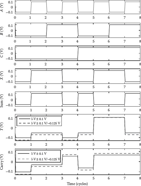
FIGURE 12.18 Simulated output response of the GPG-based full adder. D. Wolpert et al., General purpose logic gate using ballistic nanotransistors, Proc. 11th IEEE Conf. Nanotechnol., Portland, OR, p. 4, © (August 2011) IEEE. With permission.)
The BDT is proposed as a high-speed supplement to conventional Si MOSFET systems. As the BDT process matures and new logic structures and circuits are created, the remaining challenges are those of integration. One possible way of combining the BDT with silicon CMOS would be through three-dimensional integration of heterogeneous wafers, which have been previously proposed to link optical I/O and CMOS logic [11]. One example of this heterogeneous integration is shown in Figure 12.19, with high-performance BDT cores interfacing with a conventional Si CMOS chip using through-wafer vias. To integrate BDTs and MOSFETs, the voltage ranges must be shifted from ±0.15 V to a full-swing CMOS range, which will require a more complex circuit than the conventional level shifters commonly used in CMOS technologies.
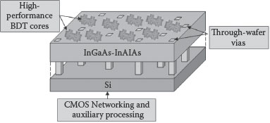
FIGURE 12.19 Heterogeneous integration of BDT cores and conventional Si CMOS.
Using this type of configuration, BDTs could provide terahertz-frequency accelerator cores for existing chip-multiprocessors. Further into the future, the BDT may take on the role of general-purpose computation, using the higher-density conventional CMOS devices purely for networking (and even this may eventually be replaced by optical I/O) and other tasks with lower-frequency requirements.
12.6 LIMITATIONS AND POTENTIAL SOLUTIONS
The BDT, like all nanoscale devices, is susceptible to a variety of variations in fabrication. In addition, the mode of operation presented in this chapter requires pull-up potentials to ensure current flow. These issues, and potential solutions to these issues, are discussed in this section.
Device variations have large impacts on leakage current and switching behavior. This chapter reports the results from three chips—a BDT device chip (Figure 12.4), a chip for the two-BDT NAND gates (Figure 12.9), and a chip for the GPGs (Figure 12.13).
Among the three chips, leakage currents vary between 0.4 and 20 μA with only up to 10% of this leakage current between the source and the top drain. Gate leakage in these devices is related to the etch depth of the trench between the gate and the channel; if the etch depth is too shallow, high-energy electrons can escape the 2DEG layer and tunnel underneath the trench, resulting in gate leakage. Unfortunately, the steepness of the trench walls is limited by the fabrication process; thus, if the trenches are made too deep, it will increase the gate–channel separation, reducing the steering capability of the device.
The Ion/Ioff ratios in the three chips vary between 1.4 and 10. The switching capability of the BDT may be improved by adjusting the geometry parameters such as the triangle location and the corner radius in the central area of the BDT [47].
BDT circuits are also susceptible to variations in resistance values in the current-to-voltage converters. Figure 12.20 shows the impact of systematic resistance variations of up to ±20% on the output voltages for logic high (Vout,high) and logic low (Vout,low). The horizontal dashed lines indicate the ideal values of the output voltages, showing that resistance variations can have a significant impact on the BDT noise window. The impact of a 20% variation in resistance can impact the output voltage by as much as 60%.
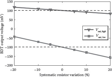
FIGURE 12.20 Impact of systematic resistor variations on the BDT output voltage.
12.6.2 ALTERNATIVE BDT CONNECTION METHODS
One potential solution to the resistor variation issue is to use an alternative method of connecting the gates together, for example, operating the BDT in a voltage mode where the outputs are directly connected to the next logic stage rather than by using current-to-voltage converters. This would eliminate the need for all the resistors in Figure 12.17a, greatly reducing the design complexity and area. An example of a BDT operating in the voltage mode is shown in Figure 12.21. Thus far, the differential output voltage generated is only 15% of the differential input voltage (over the range of input voltages between ±50 and ±300 mV); however, we expect the output response to improve significantly as device designs are optimized for this mode. An additional alternative of connecting the BDTs is to use complementary structures such as those presented in Ref. [52].
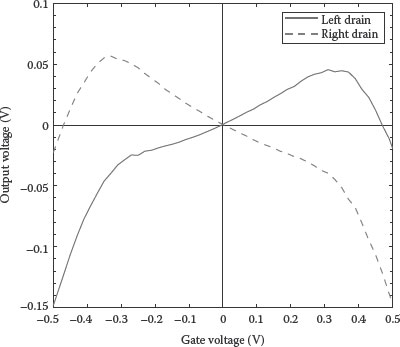
FIGURE 12.21 Voltage-mode operation of a BDT showing output voltages generated by a ±0.5 V range of differential input voltages.
12.6.3 FUTURE CIRCUIT IMPROVEMENTS
At the circuit level, the two main areas of improvement we are currently researching are the new gate structures and the new methods of connecting BDTs. The GPG concept could be extended to a 7-BDT three-gate input GPG (with the additional BDTs connected to the drains of the outer two BDTs in Figure 12.10); however, the number of devices that may be cascaded with a single 2DEG channel is limited by the mean free path, as described in Section 12.3. This 7-BDT structure would be able to perform the half-adder operation using two gates instead of five (although the BDT count would only be reduced by one); more importantly, these larger structures would dramatically reduce the wiring complexity of BDT circuits.
This chapter has described the circuit applications of a newly developed nanodevice, termed the ballistic deflection transistor (BDT), which promises terahertz performance at moderate voltages. With the successful fabrication of a set of BDT logic gates and a preliminary circuit design methodology, the BDT has the potential for consideration in the next generation of nanoscale devices. In particular, the GPG may provide a new integration opportunity for mass fabrication. A full adder has been presented as a case study on using multiple GPGs to develop circuits based on BDTs.
The presented overview of nanoscale devices reveals a number of exciting options with the potential of replacing conventional CMOS when further scaling becomes too costly. This wide variety of options may in fact introduce unexpected system complexities, as there may not be a single “predominant” device in which the resources are pooled, as was the case when CMOS emerged as the electronics standard of sorts. A number of conventional improvements may be combined, such as strained-Si channels with finFET gates, to extend the reach of conventional devices; however, these improvements do not offer the same potential performance enhancement as nonconventional ideas such as molecular or optical computing. The ballistic deflection transistor provides an interesting middle ground, pairing a mature semiconductor technology with nonconventional device and circuit design. The presented circuit design methodology points out a few complexities that must be addressed prior to adoption (such as logic depth and signal degradation), but overall the potential performance benefits of the BDT make it a strong candidate for use in the next era of computing—heterogeneous integration of nanoelectronics and CMOS. Continued work on improving the device, along with the BDT logic and circuit design, should help to further differentiate it from other alternatives.
The authors would like to thank other members of the BDT group at the University of Rochester and the University of Massachusetts at Lowell. BDT fabrication was performed at the Cornell Nanofabrication Facility (CNF), a member of the NSF-sponsored NNI network.
1. D. Wolpert, H. Irie, R. Sobolewski, P. Ampadu, Q. Diduck, and M. Margala, Ballistic deflection transistors and the emerging nanoscale era, Proc. IEEE Int. Symp. Circuits Syst., Taipei, Taiwan, pp. 61–64, May 2009.
2. W. Haensch et al., Silicon CMOS devices beyond scaling, IBM J. Res. Dev., 50(4/5), 339–361, Jul./Sept. 2006.
3. T. Skotnicki, J. Hutchby, T.-J. King, H.-S. Wong, and F. Boeuf, The end of CMOS scaling: Toward the introduction of new materials and structural changes to improve MOSFET performance, IEEE Circuits Devices Mag., 21(1), 16–26, Jan./Feb. 2005.
4. K. Ronse et al., Lithography options for the 32 nm half pitch node and beyond, IEEE Trans. Circuits Syst.-I: Regular Papers, 56(8), 1883–1890, Aug. 2009.
5. T. Oka et al., Advanced performance of small-scaled InGaP/GaAs HBT’s with fT over 150 GHz and fmax over 250 GHz, Int. Electron Devices Mtg. (IEDM’98), San Francisco, CA, pp. 653–656, Dec. 1998.
6. M. Bohr, The evolution of scaling from the homogeneous era to the heterogeneous era, IEEE Int. Elec. Dev. Mtg. (IEDM’11), Washington, DC, 1.1.1–1.1.6, Dec. 2011.
7. M. Lee, E. Fitzgerald, M. Bulsara, M. Currie, and A. Lochtefeld, Strained Si, SiGe, and Ge channels for high-mobility metal-oxide-semiconductor field-effect transistors, J. Appl. Phys., 97 011101–1–011101–28, 2005.
8. I. Ferain, C. Colinge, and J.P. Colinge, Multigate transistors as the future of classical metal-oxide-semiconductor field-effect transistors, Nature 479, 310–316, Nov. 2011.
9. S. Mujumdar, Layout-dependent strain optimization for p-channel trigate transistors, IEEE Trans. Elec. Dev., 59(1), 72–78, Jan. 2012.
10. V.F. Pavlidis and E. G. Friedman, Three-Dimensional Integrated Circuit Design, Burlington, MA: Morgan Kaufmann, 2008.
11. K. Banerjee, S. J. Souri, P. Kapur, and K. C. Saraswat, 3-D ICs: A novel chip design for improving deepsubmicrometer interconnect performance and systems-on-chip integration, Proc. IEEE, 89(5), 602–633, May 2001.
12. J. Mateos et al., Microscopic modeling of nonlinear transport in ballistic nanodevices, IEEE Trans. Elec. Dev., 50(9), 1897–1905, Sept. 2003.
13. H. Irie and R. Sobolewski, Picosecond electric pulse excitation of three-branch ballistic nanodevices, J. Phys.: Conf. Series, 193(012097), 1–4, 2009.
14. Q. Diduck, M. Margala, and M. J. Feldman, Terahertz transistor based on geometrical deflection of ballistic current, Proc. IEEE MTT-S Int. Microwave Symp., San Francisco, CA, pp. 345–347, Jun. 2006.
15. M. Stan, P. Franzon, S. Goldstein, J. Lach, and M. Ziegler, Molecular electronics: From devices and interconnect to circuits and architecture, Proc. IEEE, 91(11), 1940–1957, Nov. 2003.
16. A. E. Kaloyeros et al., Conformational molecular switches for post-CMOS nanoelectronics, IEEE Trans. Circuits Syst.-I: Regular Papers, 54(11), 2345–2352, Nov. 2007.
17. P.J. Kuekes, Molecular crossbar latch, U.S. Patent No. 6,586,965, Jul. 2003.
18. T. Palacios, Applied physics: Nanowire electronics comes of age, Nature 481, 152–153, Jan. 2012.
19. A.K. Geim and K. S. and Novoselov, The rise of graphene, Nat. Mater., 6 183–191, 2007.
20. D. Akinwanede, Y. Nishi, and H.-S. P. Wong, Carbon nanotube quantum capacitance for nonlinear terahertz circuits, IEEE Trans. Nanotechnol., 8(1), 31–36, Jan. 2009.
21. S.O. Koswatta, D. E. Nikonov, and M. S. Lundstrom, Computational study of carbon nanotube p-i-n tunnel FETs, Int. Elec. Dev. Mtg. (IEDM’05), Washington, DC, pp. 525–528, Dec. 2005.
22. A. Raychowdhury and K. Roy, Carbon nanotube electronics: Design of high-performance and low-power digital circuits, IEEE Trans. Circuits Syst.-I: Regular Papers, 54(11), 2391–2401, Nov. 2007.
23. J. Zhang, N. P. Patil, and S. Mitra, Design guidelines for metallic-carbon-nanotube-tolerant digital logic circuits, Proc. Design Automation Test Europe (DATE’08), Munich, Germany, pp. 1009–1014, Mar. 2008.
24. M. Kastner, The single electron transistor and artificial atoms, Ann. Phys., 9(11–12), 885–894, Nov. 2000.
25. G. Zardalidis and I. G. Karafyllidis, SECS: A new single-electronic-circuit simulator, IEEE Trans. Circuits Syst.-I: Regular Papers, 55(9), 2774–2784, Oct. 2008.
26. K.K. Likharev, Single-electron devices and their applications, Proc. IEEE, 87(4), 606–632, Apr. 1999.
27. S. Sarma, Ferromagnetic semiconductors: A giant appears in spintronics, Nat. Mater., 2, 292–294, May 2003.
28. S.A. Wolf, A. Y. Chtchelkanova, and D. M. Treger, Spintronics–a retrospective and perspective, IBM J. Res. Dev., 50(1), 101–110, Jan. 2006.
29. G. Bourianoff, J. E. Brewer, R. Cavin, J. A. Hutchby, and V. Zhirnov, Boolean logic and alternative information-processing devices, Computer, 41(5), 38–46, May 2008.
30. L.M. Adleman, Molecular computation of solutions to combinatorial problems, Science, 266(11), 1021–1024, Nov. 1994.
31. S. M. R. Hasan, A novel mixed-signal integrated circuit model for DNA-protein regulatory genetic circuits and genetic state machines, IEEE Trans. Circuits Syst.-I: Regular Papers, 55(5), 1185–1196, Jun. 2008.
32. H. Hug and R. Schuler, Strategies for the development of a peptide computer, Bioinformatics, 17(4), 364–368, 2001.
33. D.P. DiVincenzo, Quantum computation, Science, 270(5234), 255–261, Oct. 1995.
34. J. H. Kim et al., All-optical logic gates using semiconductor optical-amplifier-based devices and their applications, J. Korean Phys. Soc., 45(5), 1158–1161, Nov. 2004.
35. S. Datta, Electronic Transport in Mesoscopic Systems, Cambridge, UK: Cambridge University Press, 2005.
36. A. Song, Room temperature ballistic nanodevices, Encycl. Nanosci. Nanotechnol., 9, 371–389, 2004.
37. C. W. J. Beenakker and H. Van Houten, Quantum transport in semiconductor nanostructures, Solid State Phys., 44, 1–111, 1991.
38. T. Mimura, S. Hiyamizu, T. Fujii, and K. Nanbu, A new field-effect transistor with selectively doped GaA/n-AlxGa1-xAs heterojunctions, Jpn. J. Appl. Phys., 19(L225–7), 1980.
39. Y. Hirayama and S. Tarucha, High temperature ballistic transport observed in AlGaAs/InGaAs/GaAs small four-terminal structures, Appl. Phys. Lett., 63(17), 2013–2017, 1993.
40. C. W. J. Beenakker and H. Van Houten, Billiard model of a ballistic multiprobe conductor, Phys. Rev. Lett., 63(17), 1857–1860, 1989.
41. J. S. Galloo et al., Ballistic GaInAs/AlInAs devices technology and characterization at room temperature, Proc. 4th IEEE Conf. Nanotechnol. (NANO’04), Munich, Germany, 98–100, Aug. 2004.
42. T. Palm and L. Thylen, Analysis of an electron-wave Y-branch switch, Appl. Phys. Lett., 60(2), 237–239, Jan. 1992.
43. S. Reitzenstein, L. Worschech, and A. Forchel, A novel half-adder circuit based on nonometric ballistic Y-branched junctions, IEEE Elec. Dev. Lett., 24(10), 625–627, 2003.
44. H.Q. Xu, Electrical properties of three-terminal ballistic junctions, Appl. Phys. Lett., 78, 2064–2066, 2001.
45. R. Fleischmann and T. Geisel, Mesoscopic rectifiers based on ballistic transport, Phys. Rev. Lett., 89, 016804-1–016804–4, Jun. 2002.
46. H. Irie, Q. Diduck, M. Margala, R. Sobolewski, and M. J. Feldman, Nonlinear characteristics of T-branch junctions: Transition from ballistic to diffusive regime, Appl. Phys. Lett., 93, 053502, 2008.
47. D. Huo, Q. Yu, D. Wolpert, and P. Ampadu, A simulator for ballistic nanostructures in a 2-D electron gas, ACM J. Emerging Technol. Computing Syst. (JETC), 5(1), 5.1–5.21, Jan. 2009.
48. D. Wolpert, Q. Diduck, and P. Ampadu, NAND gate design for ballistic deflection transistors, IEEE Trans. Nanotechnol., 10(1), 150–154, Jan. 2011.
49. D. Wolpert, I. Iniguez-de-la-Torre, V. Kaushakl, M. Margala, and P. Ampadu, General purpose logic gate using ballistic nanotransistors, Proc. 11th IEEE Conf. Nanotechnol., Portland, OR, pp. 1171–1176, Aug. 2011.
50. T. Jhaveri et al., Maximization of layout printability/manufacturability by extreme layout regularity, J. Micro/Nanolith. MEMS MOEMS, 6(031011), Sept. 2007.
51. B.J. Lin, Future of multiple e-beam direct-write systems, Proc. 4th SPIE Conf. Alternative Lithographic Technologies, San Jose, CA, 832302, Feb. 2012.
52. T. Palm and L. Thylen, Designing logic functions using an electron waveguide Y-branch switch, J. Appl. Phys., 79(10), 8076–8081, May 1996.