
Validation of Nano-CMOS Predictive Technology Model Tool on NanoHUB.org |
CONTENTS
Next-generation electronic systems will need to adopt novel nano-electronic solutions to keep pace with Moore’s law. Nano-CMOS (complementary metal–oxide–semiconductor) technology is among the most promising of nanotechnologies. Although most new nano-electronic technologies are still in their infancy, however, they present the potential for unprecedented levels of integration, low-power computing, signal processing, information storage, and possibly higher operating frequency with cost-effective system solution [1,2]. Advanced MOSFET (metal–oxide–semiconductor field-effect transistor) structures show a promise for scaling CMOS technology to gate lengths below 10 nm to enable continued improvements in integrated circuit (IC) cost and performance (e.g., higher operating speed) for at least 10 more years. Over the past three decades, by reducing the transistor gate lengths with each new generation of manufacturing technology, steady improvements in circuit performance (speed) and cost per function have been reported [2]. However, continued transistor scaling will not be as straightforward in the future as it has been in the past because the fundamental materials and process limits are rapidly being approached.
The challenge of extending Moore’s law beyond the physical and economic barriers of the present semiconductor technologies calls for novel nano-electronic solutions. Silicon-based CMOS technology can be scaled down into the nanometer regime. High-performance, planar, ultrathinbody devices fabricated on silicon-on-insulator substrates have been demonstrated down to 15-nm gate lengths [1,2]. The effects of crystal orientation and roughness on carrier mobility, gate work function engineering, circuit performance, and sensitivity to process-induced variations are the critical factors to design nanoscale devices [3,4]. In this research, nano-CMOS models are investigated to analyze the CMOS behavior at the nanoscale. The importance of physical correlations among the parameters and the impact of process variations have been evaluated. An HSPICE (Simulation Program with Integrated Circuit Emphasis) model file is converted into a PSPICE format. Different models and parameters are investigated using BSIM 4 and BSIM 3 models. Various CMOS gates in a nanoscale are simulated and the results are analyzed. To predict the effect of temperature, the team simulated 32 and 65 nm CMOS gates. The temperature varied from 0°C to 1000°C in 10° increments. Predictive technology model (PTM) files estimate the behavior of submicron transistors. The files are generated by scaling down from larger known technology nodes. To facilitate the extraction of PTMs, online tools such as the nano-CMOS tool in http://NanoHUB.org are available for free to the public. This tool allows a user to automatically generate a model card by adjusting 10 parameters. Modifying the temperature parameter gives a new look into how submicron transistors will behave at high temperatures. Extensive research has been carried out into the design of PTM files for transistors in the submicron range [5]. Since PTM files can be used in conjunction with CAD (computer-aided design) programs, circuit designers are able to characterize nano-CMOS circuits even before the technology is available for manufacturing. Therefore, it is very important that the model files are as accurate as possible. An important aspect of circuit design is the knowledge on how a circuit will perform in high temperatures; yet, the extraction of PTM files at different temperatures other than room temperature is an area that has not been fully explored.
As mentioned above, one of the tools available to the nano-community is the nano-CMOS tool available in http://NanoHUB.org [6]. This tool allows a user to automatically generate a model card by adjusting 10 parameters. These parameters are physical gate length (LEFF), LEFF variation percentage, threshold voltage (VTH), VTH variation, power supply voltage (VDD), equivalent electrical oxide thickness (TOX), total source and drain series resistance (Rdsw), number of bias points in Vgs and Vds, and temperature (TNOM).
In this research, the main parameter of interest is TNOM. The ability to modify TNOM is a new feature added to the nano-CMOS tool on http://NanoHUB.org. This feature is not available in the original nano-CMOS tool [7]. TNOM corresponds to the temperature at which the model card parameters are extracted. To test the effects of modifying the TNOM parameter, various CMOS gates such as ninestage inverter, NAND, NOR, XOR are designed in SPICE to observe the effects of temperature when: (1) only the TNOM parameter is varied, (2) only the circuit simulation temperature (TCIRCUIT) is varied, and (3) both TNOM and TCIRCUIT are set to match accordingly. Measurements are taken for all three trials at 27°C and 125°C.
The chapter is organized as follows: Section 1.2 gives an overview of the tool used including its features and limitations. Section 1.3 explains about the model cards generated along with the I–V curves extracted using the tool at both 27°C and 125°C for various transistor sizes used in the simulations. Section 1.4 summarizes the methodology used for research and Section 1.5 draws some conclusions and future research.
Nano-CMOS is an online tool developed by the Nanoscale Integration and Modeling (NIMO) Group at Arizona State University. It is designed to provide the users an easy method to customize the model file to whatever technology specifications they desire. The user is limited to the following constraints when using the tool:
• Designed only for bulk-CMOS.
• Able to simulate for physical gate length down to 10 nm and up to 145 nm.
• Temperature ranges input can be from 70 to 450 K (−203−177°C).
• Total source and drain series resistance input can be between 90 and 300 Ω-μm.
• Equivalent electrical oxide thickness can be from 0.8 to 1.8 nm.
• Power supply voltage can be between 0.7 and 1.8 V.
• Threshold voltage can be between −0.4 and 0.4 V.
• Allowable variation of threshold voltage can be between −100 and 100 mV.
• Model files are designed to work with SPICE programs compatible with BSIM4.
TABLE 1.1
Model Parameters for 32 and 65 nm Technology Nodes
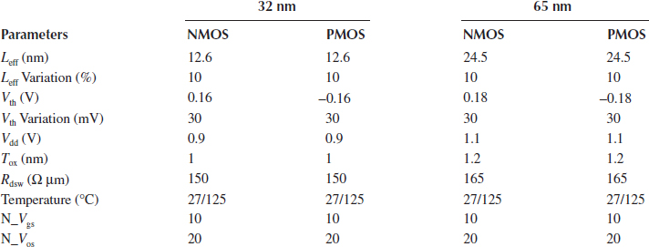
Source: W. Zhao, and Y. Cao, New generation of predictive technology model for sub-45 nm design exploration, Proceedings of the IEEE International Symposium on Quality Electronic Design, San Jose, CA, pp. 585—590 © (March 2006) IEEE. With permission; W. Zhao, and Y. Cao, ACM Journal on Emerging Technologies in Computing Systems (JETC), 3(1): 1–17, April 2007. With permission.
The preconfigured bulk-CMOS model files include the nominal, slow–slow corner, and fast–fast corner model files for 32 nm PMOS (p-channel metal-oxide-semiconductor) and NMOS (n-channel metal-oxide-semiconductor), 45 nm PMOS and NMOS, 65 nm PMOS and NMOS, 90 nm PMOS and NMOS, and 130 nm PMOS and NMOS.Table 1.1 shows the parameters used to generate the model files.
Alternately, the IV curves for the PMOS transistors show that the current increases as the voltage increases, even at higher temperatures. For all instances of the IV curves in the subthreshold region, we observe that the currents at the higher and lower temperatures are approximately the same.
Model cards are extracted for different temperatures. This is easily accomplished using the nano-CMOS tool. Then the four logic gates are designed in a SPICE program to measure the propagation delay of the output when the temperature is set at 27°C and 125°C. Three different configurations are used to add the effects of temperature in a circuit.
A basic CMOS inverter, NAND, NOR, and XOR gates are designed in conjunction with the model files. All the CMOS gates are simulated using HSPICE. Figure 1.1 shows a nine-stage inverter circuit. The input voltage starts at 0 V and then increases to 1.8 V.
It is expected that the slow–slow corner is run at a slower speed, but has the best performance; the fast–fast corner is run at a higher speed, but shows the worst performance, and the nominal shows balanced performance between the two in terms of speed and performance. It is also observed that the larger technology nodes (90 and 130 nm) showed better performance in terms of rise time and fall time when compared to the small technology nodes (32 and 45 nm). The above-mentioned model parameters are included in PSPICE simulation and the temperature-dependent critical parameters are identified for simulation. Once the user adjusts the parameters to the desired technology node and simulates, the tool can output the IV curves of the nominal transistor in the linear and saturation region, the IV curves in the subthreshold region, and the HSPICE code for the nominal transistor model, the slow–slow corner transistor model, and the fast–fast corner transistor model. The generated code can be modified for any SPICE software that supports BSIM4.
The model files used in the simulation are generated by using the parameters listed in Table 1.1. Those values are determined through a review of the literature [5]. They are also the default values set on the nano-CMOS tool for their respective technology nodes. For each of the four transistors (32 nm NMOS and PMOS, 65 nm NMOS and PMOS), the IV curves are generated to get a look at the current versus the voltage at 27°C and 125°C. The IV curves show the MOSFET operations in the triode and saturation regions. In addition, the IV curves in the logarithmic scales are shown for each MOSFET. The IV curves are shown in Figures 1.2 through 1.9. It is observed from the graphs that the NMOS transistor’s current is lower in the triode region due to an increase of Rds at a higher temperature. Eventually, the current at higher temperatures increases even at higher voltage (Vds) levels.
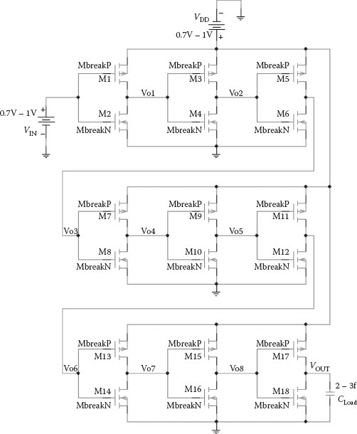
FIGURE 1.1 Nine-stage inverter circuit.
Alternately, the IV curves for the PMOS transistors show that the current increases as the voltage increases, even at higher temperatures. For all instances of the IV curves in the subthreshold region, we observe that the currents at the higher and lower temperatures are approximately the same.
1.4 METHODOLOGY
Model cards are extracted for different temperatures. This is easily accomplished using the nano-CMOS tool. Then the four logic gates are designed in a SPICE program to measure the propagation delay of the output when the temperature is set at 27°C and 125°C. Three different configurations are used to add the effects of temperature in a circuit.
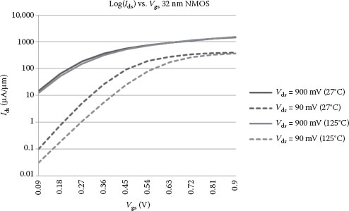
FIGURE 1.2 ID–VG curves for 32 nm NMOS. (A. Rodriguez and H. F. Huq, Validation of Nano-CMOS Predictive Technology Model Tool on NanoHUB.org., IEEE International Conference on Nanotechnology, Portland, OR, pp. 469–472, August 15–18, © (2011) IEEE. With permission.)
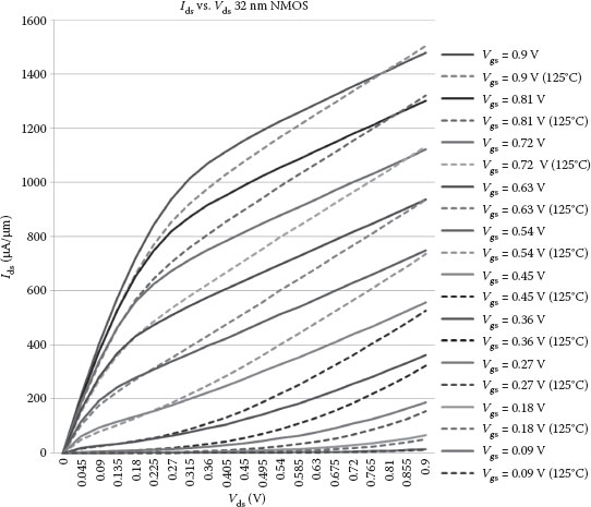
FIGURE 1.3 ID–VD curves for 32 nm NMOS. (A. Rodriguez and H. F. Huq, Validation of Nano-CMOS Predictive Technology Model Tool on NanoHUB.org., IEEE International Conference on Nanotechnology, Portland, OR, pp. 469–472, August 15–18, © (2011) IEEE. With permission.)
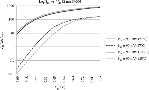
FIGURE 1.4 ID–VG curves for 32 nm PMOS. (A. Rodriguez and H. F. Huq, Validation of Nano-CMOS Predictive Technology Model Tool on NanoHUB.org., IEEE International Conference on Nanotechnology, Portland, OR, pp. 469–472, August 15–18, © (2011) IEEE. With permission.)
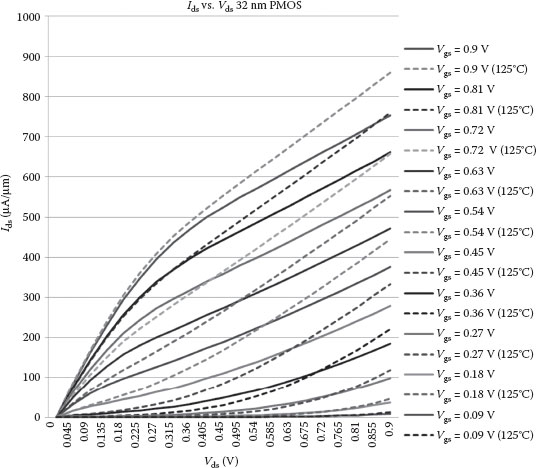
FIGURE 1.5 ID–VD curves for 32 nm PMOS. (A. Rodriguez and H. F. Huq, Validation of Nano-CMOS Predictive Technology Model Tool on NanoHUB.org., IEEE International Conference on Nanotechnology, Portland, OR, pp. 469–472, August 15–18, © (2011) IEEE. With permission.)
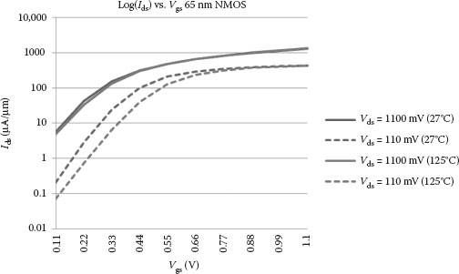
FIGURE 1.6 Log IV curves for 65 nm NMOS. (A. Rodriguez and H. F. Huq, Validation of Nano-CMOS Predictive Technology Model Tool on NanoHUB.org., IEEE International Conference on Nanotechnology, Portland, OR, pp. 469–472, August 15–18, © (2011) IEEE. With permission.)
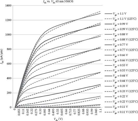
FIGURE 1.7 IV curves for 65 nm NMOS. (A. Rodriguez and H. F. Huq, Validation of Nano-CMOS Predictive Technology Model Tool on NanoHUB.org., IEEE International Conference on Nanotechnology, Portland, OR, pp. 469–472, August 15–18, © (2011) IEEE. With permission.)
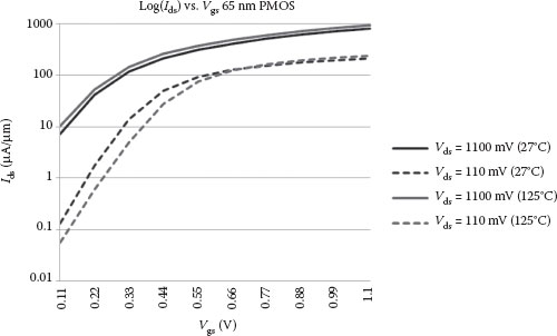
FIGURE 1.8 Log IV curves for 65 nm PMOS. (A. Rodriguez and H. F. Huq, Validation of Nano-CMOS Predictive Technology Model Tool on NanoHUB.org., IEEE International Conference on Nanotechnology, Portland, OR, pp. 469–472, August 15–18, © (2011) IEEE. With permission.)
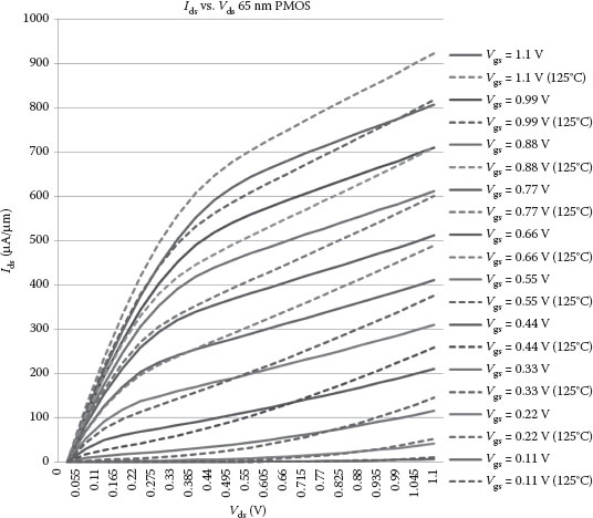
FIGURE 1.9 IV curves for 65 nm PMOS. (A. Rodriguez and H. F. Huq, Validation of Nano-CMOS Predictive Technology Model Tool on NanoHUB.org., IEEE International Conference on Nanotechnology, Portland, OR, pp. 469–472, August 15–18, © (2011) IEEE. With permission.)
• In the first configuration, the TNOM parameter from nano-CMOS is varied to observe the effects of the performance of the circuits. When running the simulation, TCIRCUIT is left at room temperature (27°C).
• The second configuration used the model files extracted at room temperature and varied the TCIRCUIT parameter of the SPICE program.
• The third setup is a combination of the previous scenarios where both TNOM and TCIRCUIT are set to 27°C, then again at 125°C.
It is expected that a transistor should perform slower at a higher temperature [8]. The characteristics of the IV curves show that once the voltage (Vds) gets close to its maximum value, the performance of the transistors at different temperatures is only slightly different. Therefore, it is not expected for the performance degradation at the higher temperature to be of a great amount. We hypothesize that the third configuration will generate the most accurate trials in these simulations. The results from the simulations are shown in Tables 1.2 through 1.5. After analyzing the results, we observe a consistent trend among all the simulation results. When only TNOM is varied, the results show a decrease in propagation delay as the temperature increases. This goes against the standard behavior of propagation delay with temperature, but this type of outcome is suggested as a possibility in Ref. [9].
TABLE 1.2
Propagation Delays for CMOS NOT Simulation Results
Nine-Stage Inverter |
||||
Temperature Change |
PTM (nm) |
Average Propagation Delay(s)—27°C |
Average Propagation Delay(s)—125°C |
Variation % |
Tnom (Nano-CMOS) |
32 |
1.326E–10 |
1.226E–10 |
7.57918552 |
65 |
1.658E–10 |
1.359E–10 |
18.03377563 |
|
Tcircuit (SPICE) |
32 |
1.335E–10 |
1.870E–10 |
–40.1273885 |
65 |
1.646E–10 |
2.420E–10 |
–47.0677606 |
|
Tnom and Tcircuit |
32 |
1.335E–10 |
1.552E–10 |
–16.2607718 |
65 |
1.646E–10 |
1.625E–10 |
1.245821939 |
|
Source: A. Rodriguez and H. F. Huq, Validation of Nano-CMOS Predictive Technology Model Tool on http://NanoHUB.org., IEEE International Conference on Nanotechnology, Portland, OR, pp. 469–472, August 15–18, © (2011) IEEE. With permission.
TABLE 1.3
Propagation Delays for CMOS NAND Simulation Results
NAND |
||||
Temperature Change |
PTM (nm) |
Average Propagation Delay(s)—27°C |
Average Propagation Delay(s)—125°C |
Variation % |
Tnom (Nano-CMOS) |
32 |
1.397E–10 |
1.315E–10 |
5.871822413 |
65 |
1.478E–10 |
1.257E–10 |
14.92385787 |
|
Tcircuit (SPICE) |
32 |
1.404E–10 |
1.919E–10 |
–36.6809117 |
65 |
1.485E–10 |
2.042E–10 |
–37.5084175 |
|
Tnom and Tcircuit |
32 |
1.404E–10 |
1.639E–10 |
–16.7378917 |
65 |
1.485E–10 |
1.604E–10 |
–7.97979798 |
|
Source: A. Rodriguez and H. F. Huq, Validation of Nano-CMOS Predictive Technology Model Tool on http://NanoHUB.org., IEEE International Conference on Nanotechnology, Portland, OR, pp. 469–472, August 15–18, © (2011) IEEE. With permission.
TABLE 1.4
Propagation Delays for CMOS NOR
NOR |
||||
Temperature Change |
PTM (nm) |
Average Propagation Delay(s)—27°C |
Average Propagation Delay(s)—125°C |
Variation % |
Tnom (Nano-CMOS) |
32 |
1.519E–10 |
1.351E–10 |
11.05990783 |
65 |
1.499E–10 |
1.217E–10 |
18.81881882 |
|
Tcircuit (SPICE) |
32 |
1.535E–10 |
2.333E–10 |
–52.036494 |
65 |
1.510E–10 |
2.276E–10 |
–50.6953642 |
|
Tnom and Tcircuit |
32 |
1.535E–10 |
1.784E–10 |
–16.2593679 |
65 |
1.510E–10 |
1.527E–10 |
–1.09271523 |
|
Source: A. Rodriguez and H. F. Huq, Validation of Nano-CMOS Predictive Technology Model Tool on http://NanoHUB.org., IEEE International Conference on Nanotechnology, Portland, OR, pp. 469–472, August 15–18, © (2011) IEEE. With permission.
TABLE 1.5
Propagation Delays for CMOS XOR
XOR |
||||
Temperature Change |
PTM (nm) |
Average Propagation Delay(s)—27°C |
Average Propagation Delay(s)—125°C |
Variation % |
Tnom (Nano-CMOS) |
32 |
1.811E–10 |
1.647E–10 |
9.083379348 |
65 |
1.790E–10 |
1.423E–10 |
20.50852193 |
|
Tcircuit (SPICE) |
32 |
1.822E–10 |
2.781E–10 |
–52.6344676 |
65 |
1.802E–10 |
2.708E–10 |
–50.2774695 |
|
Tnom and Tcircuit |
32 |
1.822E–10 |
2.210E–10 |
–21.2952799 |
65 |
1.807E–10 |
1.833E–10 |
–1.41117875 |
|
Source: A. Rodriguez and H. F. Huq Validation of Nano-CMOS Predictive Technology Model Tool on http://NanoHUB.org., IEEE International Conference on Nanotechnology, Portland, OR, pp. 469–472, August 15–18, © (2011) IEEE. With permission.)
When only the temperature is modified in the SPICE file, we see that there is a drastic reduction in the performance at a higher temperature concurrent with the behavior observed in Ref. [10]. The last variation has not been tested previously. Results show a moderate and slight degradation in the performance at a higher temperature for the 32 and 65 nm nodes, respectively.
As stated in Refs. [10,11], temperature-dependent parameters within the model card are the temperature coefficient for threshold voltage (KT1), channel length dependence of the temperature coefficient for threshold voltage (KT1 L), body-bias coefficient of threshold voltage temperature (KT2), temperature coefficient for UA (UA1), temperature coefficient for UB (UB1), temperature coefficient for UC (UC1), temperature coefficient for saturation velocity (AT), temperature coefficient for Rdsw (PRT), emission coefficients of junction for source and drain junctions, respectively (NJS, NJD), junction current temperature exponents for source and drain junctions, respectively (XTIS, XTID), and temperature at which parameters are extracted (TNOM). We have noticed that when modifying TNOM, four additional parameters are affected. These are long-channel threshold voltage at Vbs = 0 (VTH0), first-order body bias coefficient (K1), low-field mobility (U0), and doping concentration in the channel (NDEP). Further research needs to be performed to determine if the addition of the temperature modification field on the nano-CMOS tool leads to more accurate results at higher temperatures based on the data obtained from the TNOM and TCIRCUIT trials. In addition, the significance of the additional four parameters that change with TNOM needs to be studied.
The authors wish to thank the NIMO group at Arizona State University for the valuable insight on the nano-CMOS tool.
1. L. Chang, Y.-K. Choi, D. Ha, P. Ranade, S. Xiong, J. Boker, C. Hu, and T.-J. King, Extremely scaled silicon nano-CMOS devices, invited paper, Proceedings of the IEEE, 91(11), Nov. 2003.
2. M. M. Ziegler, and M. R. Stan, CMOS/nano co-design for crossbar-based molecular electronic systems, IEEE Transactions on Nanotechnology, 2(4), 217–230, Dec. 2003.
3. X. Liu, C. Lee, and C. Zhou, Carbon nanotube field-effect inverters, Applied Physics Letters, 79(20), 3329–3331, Nov. 2001.
4. Y. Cui, Z. Zhong, D. Wang, W. U. Wang, and C. M. Lieber, High performance silicon nanowire field effect transistors, Nano Letters, 3(2), 149–152, 2002.
5. W. Zhao, and Y. Cao, New generation of predictive technology model for sub-45 nm design exploration, Proceedings of the IEEE International Symposium on Quality Electronic Design, San Jose, CA, pp. 585–590, March 2006.
6. W. Zhao, and Y. Cao, Predictive technology model for nano-CMOS design exploration, ACM Journal on Emerging Technologies in Computing Systems (JETC), 3(1), 1–17, April 2007.
7. Predictive Technology Model (PTM), http://www.eas.asu.edu/~ptm/
8. S. Sedra, and K.C. Smith, Microelectronic Circuits (5th edition). New York: Oxford, 2004.
9. R. Kumar, and V. Kursun, Reversed temperature-dependent propagation delay characteristics in nanometer CMOS circuits. IEEE Transactions on Circuits and Systems, 53(10):1078–1082, Oct. 2006.
10. R. Kumar, and V. Kursun, Modeling of temperature effects on nano-CMOS devices with the predictive technologies. 50th Midwest Symposium on Circuits and Systems, MWSCAS Conference, Montreal, Canada, August 2007.
11. X. Xi et al., BSIM4.3.0 MOSFET Model-User Manual. Berkeley, CA: Dept. Elect. Comput. Eng., Univ. California, 2003.
12. A. Rodriguez and H. F. Huq, Validation of Nano-CMOS predictive technology model tool on NanoHUB. org., IEEE International Conference on Nanotechnology, August 15–18, 2011, Portland, OR, pp. 469–472.